


)
XC6420 Series
150mA Small Dual LDO Regulator with ON/OFF Switch
■GENERAL DESCRIPTION
The XC6420 series is a small dual CMOS LDO regulator with 2-channel 150mA outputs. The series features high speed,
high accuracy, high ripple rejection and low dropout voltage. The series is capable of high density board installation by the
small package of two low on-resistance regulators. Each output voltage is internally set in a range from 1.2V to 3.6V in
increments of 0.05V with ±2% accuracy.
The EN function controls the two regulators on/off independently. In the stand-by mode, the electric charge at the output
capacitor C
The series is also compatible with low ESR ceramic capacitors. The high level of output stability is maintained even during
frequent load fluctuations, due to the excellent transient response performance. The two regulators are completely isolated so
that a cross talk during load fluctuations is minimized.
■APPLICATIONS
● Mobile phones
● Portable game consoles
● Portable multimedia player
● Digital still cameras, Camcorders
■TYPICAL APPLICATION CIRCUITS
L is discharged via the internal switch and as a result the V
■FEATURES
Maximum Output Current : 150mA
Operating Voltage Range : 1.6V~5.5V
Output Voltage : 1.2V~3.6V (±2%) 0.05V increments
Dropout Voltage : 190mV @I
Low Power Consumption : 55μA / ch (TYP.)
Stand-by Current : 0.1μA
Ripple Rejection : 75dB@1kHz
EN Function : Active High
C
Protection Circuit : Current Limit 250mA (TYP.)
Short Circuit 50mA (TYP.)
Output Capacitor : 1.0μF Ceramic Capacitor
Operating Ambient Temperature : -40℃ ~ +85℃
Packages
Environmentally Friendly : EU RoHS Compliant, Pb Free
■TYPICAL PERFORMANCE
CHARACTERISTICS
pin quickly returns to the VSS level.
OUT
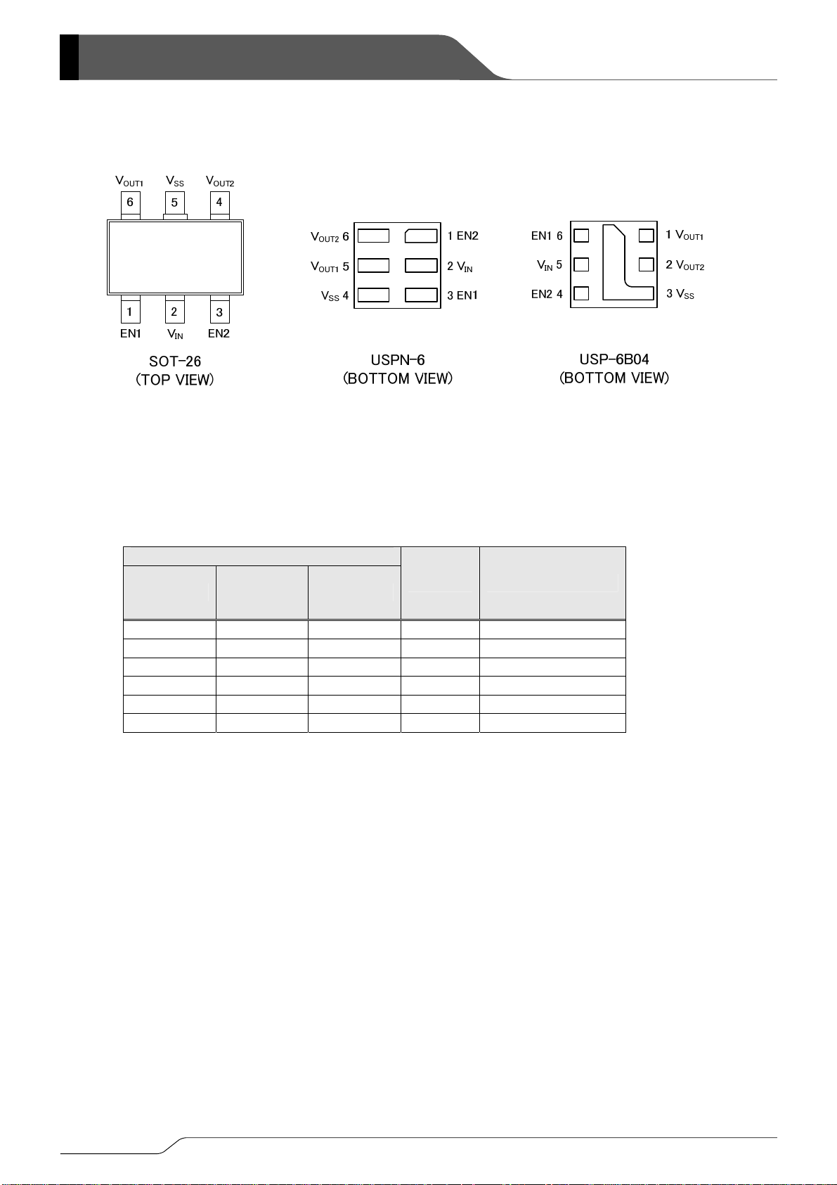
: SOT-26
USPN-6
USP-6B04
Ripple Rejection
XC6420(V
C
=0.1μF(ceramic), CL=1.0μF(ceramic
100
80
60
40
20
Ripple Rejection Rate : RR (dB)
0
0.1 1 10 100 1000
IN
IOUT=0.1mA
IOUT=1mA
IOUT=30mA
IOUT=100mA
Ripple Frequency : f (kHz)
High Speed Auto Discharge
L
=1.8V)
OUT
=3.0V+0.5V
V
IN
ETR0352-006
=150mA (V
OUT
, Ta=25℃
p- pAC
OUT
=3.3V)
1/26
XC6420 Series
■PIN CONFIGURATION
■PIN ASSIGNMENT
SOT-26 USPN-6 USP-6B04
1 3 6 EN1 ON/OFF Control 1
2 2 5 VIN Power Input
3 1 4 EN2 ON/OFF Control 2
4 6 2 V
5 4 3 VSS Ground
6 5 1 V
PIN NUMBER
PIN NAME FUNCTIONS
Output 2
OUT2
Output 1
OUT1
2/26

●
■ PRODUCT CLASSIFICATION
Ordering Information
XC6420①②③④⑤⑥-⑦
(*1)
DESIGNATOR ITEM SYMBOL DESCRIPTION
EN1: Active High, EN2: Active High
①
②
③④
Basic Function A
Enable Pin B EN1: With Pull-down, With EN2: Pull-down
Output Voltage
01~
V
: with CL Auto Discharge,
OUT1
V
: with CL Auto Discharge
OUT2
See the chart below
MR-G SOT-26 (3,000/Reel)
⑤⑥-⑦
(*1)
The “-G” suffix indicates that the products are Halogen and Antimony free as well as being fully RoHS compliant.
(*1)
Packages (Order Unit)
7R-G USPN-6 (5,000/Reel)
DR-G
USP-6B04 (5,000/ Reel)
DESIGNATOR ③④
V
③④
(V) V
OUT1
OUT2
(V)
③④
V
(V) V
OUT1
OUT2
XC6420
Series
(V)
01 1.20 1.20 31 1.50 2.80
02 1.20 1.50 32 1.80 2.80
03 1.20 2.50 33 2.80 2.80
04 1.20 2.85 34 2.80 3.00
05 1.20 3.00 35 2.80 3.30
06 1.20 3.30 36 1.20 3.60
07 1.50 1.50 37 3.60 1.20
08 1.50 1.80 38 1.20 2.80
09 1.50 2.50 39 3.30 2.00
10 1.50 2.85 40 3.00 3.30
11 1.50 3.00 41 3.30 3.30
12 1.50 3.30 42 1.30 1.50
13 1.80 1.80 43 2.60 2.80
14 1.80 2.50 44 3.10 3.30
15 2.85 2.85 45 1.50 2.60
16 1.80 2.85 46 2.60 3.30
17 1.80 3.00 47 3.40 3.40
18 3.00 1.80 48 2.85 2.60
19 1.80 3.30 49 3.30 1.80
20 2.50 2.50 50 1.80 1.20
21 2.50 2.80 51 3.10 3.10
22 2.50 2.85 52 1.50 3.10
23 3.30 1.50 53 3.30 2.80
24 2.50 3.00 54 3.00 2.80
25 2.50 3.30 55 3.30 3.00
26 2.85 3.00
27 2.85 3.30
28 3.00 3.00
29 1.20 1.80
30 1.30 2.80
*For other output voltage combinations, please contact your local Torex sales office or representative.
3/26

XC6420 Series
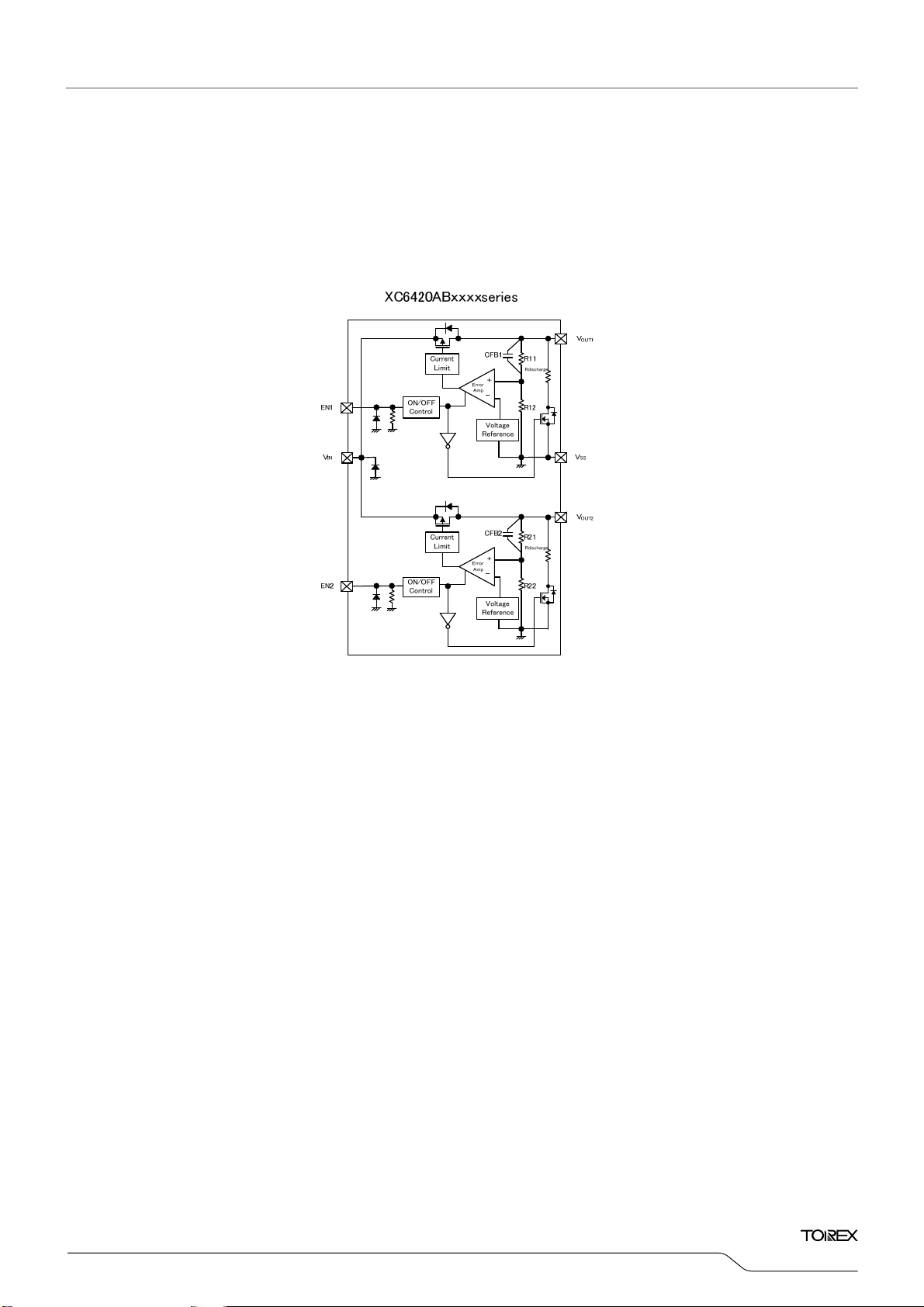
■BLOCK DIAGRAMS
■ABSOLUTE MAXIMUM RATINGS
Output Voltage 1 / Output Voltage2 V
EN1/EN2 Input Voltage V
* Diodes inside the circuits are ESD protection diodes and parasitic diodes.
PAR AMETER SYMBOL RATINGS UNITS
Input Voltage
Output Current
SOT-26
V
Vss-0.3~+7.0 V
IN
I
OUT1+IOUT2
/V
OUT1
/V
EN1
600
V
OUT2
V
EN2
SS
(*1)
mA
-0.3~VIN+0.3 V
-0.3~+7.0 V
SS
250
600 (PCB mounted)
(*2)
4/26
Power Dissipation
USPN-6
USP-6B04
Operating Ambient Temperature
Storage Temperature
(*1)
Please use within the range of Pd > { (VIN-V
(*2)
This is a reference data taken by using the test board. Please refer to 22~24 for detail information of test condition.
OUT1
Pd
600 (PCB mounted)
600 (PCB mounted)
100
(*2)
(*2)
Topr -40~+85 ℃
Tst g -55 ~+125 ℃
)×I
OUT1
+ (VIN-V
OUT2
)×I
OUT2
}
mW
XC6420
■ELECTRICAL CHARACTERISTICS
●XC6420 series
Regulator 1, Regulator 2
PAR AMETER SYMBOL CONDITIONS
Output Voltage V
Maximum Output
Current
Load Regulation ΔV
Dropout Voltage
Supply Current ISS
Stand-by Current
(*8)
(*2)
OUT(E)
I
OUTMAX
OUT
(*5)
Vdif I
I
V
STB
VEN =VIN, I
V
EN =VIN
V
=VIN
EN
0.1mA≦I
=150mA, VEN =V
OUT
V
=VIN
EN
I
=0mA
OUT
EN =VSS
OUT
=10mA
MIN. TYP. MAX.
V
OUT(T)
×0.98
(*3)
V
OUT(T)
V
(*4)
×1.02
OUT(T)
(*3)
UNITS
150 - - mA
≦150mA
OUT
IN
- 25 45 mV
See “OUTPUT VOLTAGE CHART”
- 55 105 μA
- 0.01 0.1 μA
2.5V≦VIN≦5.0V
Line Regulation
(ΔV
ΔV
OUT
IN・VOUT
(V
V
/
)
V
(V
V
≦2.0V)
OUT(T)
, I
EN=VIN
OUT(T)
EN=VIN
OUT
+0.5V≦VIN≦5.5V
≧2.05V)
OUT(T)
, I
OUT
=30mA
=30mA
- 0.02 0.1 %/V
Input Voltage VIN - 1.6 - 5.5 V
Output Voltage
Temperature
Characteristics
ΔV
OUT
(ΔTopr・V
/
V
EN
-40℃≦Ta ≦85℃
)
OUT
=VIN, I
OUT
=10mA
- ±100 -
(R&D Value)
=VIN
V
EN
Ripple Rejection Rate PSRR
Limit Current I
Short Current I
EN”H”Level Voltage V
EN”L”Level Voltage V
EN”H”Level Current I
EN”L”Level Current I
CL Discharge Resistor R
LIM
SHORT
ENH
ENL
ENH
ENL
DCHG
VEN =VIN 150 250 - mA
V
IN{VOUT(T)
I
OUT
V
EN
V
OUT=VSS
+1.0}+0.5Vp-pAC
=30mA, f=1kHz
=VIN
- 75 - dB
- 50 - mA
- 1.0 - 5.5 V
- - - 0.3 V
VEN =V
=5.5V 2.5 6.0 9.1 μA
IN
VEN =VSS -0.1 - 0.1 μA
V
=5.5V, VEN =VSS
V
IN
OUT
=2.0V
- 300 - Ω
Ta =2 5℃
CIRCUITS
V ①
mV ①
ppm
/℃
Series
①
①
②
②
①
①
①
③
①
①
①
①
①
①
①
NOTE:
Unless otherwise stated, V
(*1)V
(*2)Characteristics of the actual V
(*3)V
(*4)Vdif={V
(*5)E-1 : See the dropout voltage chart
(*6)Each channel is measured when the other channel is turned off (V
: Effective output voltage
OUT(E)
: Nominal output voltage
OUT(T)
IN1-VOUT1
V
: The input voltage when V
IN1
V
: A voltage equal to 98% of the output voltage whenever an amply stabilized I
OUT1
IN=VOUT(T)
}
+1V, I
OUT(E)
OUT1
=1mA, CIN=CL=1.0μF.
OUT
by setting output voltage is shown in the voltage chart.
appears as input voltage is gradually decreased.
EN=VSS
OUT{VOUT(T)
).
+1.0V} is input.
5/26

XC6420 Series
■OUTPUT VOLTAGE CHART
NOMINAL
OUTPUT
VOLTAGE
(V)
V
OUT(T)
OUTPUT
VOLTAGE
(V)
V
Vdif V
OUT(E)
MIN. MAX. TYP. MAX.
1.200 1.176 1.224 2.450 2.401 2.499
1.250 1.225 1.275
1.300 1.274 1.326 2.550 2.499 2.601
1.350 1.323 1.377
1.400 1.372 1.428 2.650 2.597 2.703
1.450 1.421 1.479 2.700 2.646 2.754
1.500 1.470 1.530 2.750 2.695 2.805
1.550 1.519 1.581
1.600 1.568 1.632 2.850 2.793 2.907
1.650 1.617 1.683 2.900 2.842 2.958
1.700 1.666 1.734 2.950 2.891 3.009
1.750 1.715 1.785
1.800 1.764 1.836 3.050 2.989 3.111
1.850 1.813 1.887 3.100 3.038 3.162
1.900 1.862 1.938 3.150 3.087 3.213
1.950 1.911 1.989
2.000 1.960 2.040 3.250 3.185 3.315
2.050 2.009 2.091 3.300 3.234 3.366
2.100 2.058 2.142 3.350 3.283 3.417
2.150 2.107 2.193 3.400 3.332 3.468
2.200 2.156 2.244 3.450 3.381 3.519
2.250 2.205 2.295 3.500 3.430 3.570
2.300 2.254 2.346 3.550 3.479 3.621
2.350 2.303 2.397
2.400 2.352 2.448
DROPOUT
VOLTAGE
(mV)
560 710
530 600
460 520
380 470
300 450
280 390
NOMINAL
OUTPUT
VOLTAGE
(V)
V
OUT(T)
OUTPUT
VOLTAGE
(V)
Vdif
OUT(E)
MIN. MAX. TYP. MAX.
2.500 2.450 2.550
2.600 2.548 2.652
2.800 2.744 2.856
3.000 2.940 3.060
3.200 3.136 3.264
3.600 3.528 3.672
DROPOUT
VOLTAGE
(mV)
280 390
200 340
190 270
6/26
XC6420
■OPERATIONAL EXPLANATION
The voltage divided by resistors Rx1 & Rx2 is compared with the internal reference voltage by the error amplifier. The
P-channel MOSFET connected to the V
pin is controlled & stabilized by a system of negative feedback. The current limit circuit and short protect circuit
V
OUT
pin is then driven by the subsequent output signal. The output voltage at the
OUT
operate in relation to the level of output current. Further, the IC's internal circuitry can be shutdown via the EN pin's
signal.
<Low ESR Capacitor>
The XC6420 needs an output capacitor (CL) for phase compensation. In order to ensure the effectiveness of the phase
compensation, we suggest that an output capacitor (C
VSS pin. Please use an output capacitor with a capacitance value of at least 1.0μF. Also, please place 1.0μF input
capacitor C
<Current Limiter, Short-Circuit Protection>
The XC6420 includes a combination of a fixed current limiter circuit & a foldback circuit, which aid the operations of the
current limiter and circuit protection. When the load current reaches the current limit level, the fixed current limiter circuit
operates and output voltage drops. As a result of this drop in output voltage, the foldback circuit operates, output voltage
drops further and output current decreases. When the output pin is shorted, a current of about 50mA flows.
<EN Pin>
The IC's internal circuitry can be shutdown via the signal from the EN pin with the XC6420 series. In shutdown mode, the
series enables the electric charge at the output capacitor C
V
pin, and as a result the V
SS
The EN pin is internally pulled down by a resistor. Please note that input current through a pull-down resistor exists.
between VIN and VSS pins for stabilizing input supply voltage.
L
pin quickly returns to the VSS level.
OUT
) is connected as close as possible to the output pin (V
L
<CL Auto-Discharge Function>
XC6420 series can quickly discharge the electric charge at the output capacitor (CL), when a low signal to the EN pin,
which enables a whole IC circuit put into OFF state, is inputted via the N-channel transistor located between the V
and the V
SS pin (cf. BLOCK DIAGRAM). The C
discharge resistance is set to 300Ω when VIN is 5.5V (TYP.) and V
L
2.0V (TYP.). Moreover, discharge time of the output capacitor (C
output capacitor (C
value (C
L) as τ(τ=C x R), the output voltage after discharge via the N channel transistor is calculated by the following
L). By setting time constant of a CL auto-discharge resistance value [R
formulas.
V = V
OUT(E) x e
V : Output voltage after discharge, V
τ: C
L auto-discharge resistance R
: Output voltage, t: Discharge time,
OUT(E)
×Output capacitor (CL) value C
DCHG
to be discharged via the internal switch between V
L
L) is set by the C
–t/
τ
, or t=τIn ( V
OUT(E)
auto-discharge resistance and the
L
] and an output capacitor
DCHG
/ V )
) and the
OUT
pin and
OUT
OUT pin
OUT
Series
is
7/26

XC6420 Series
■NOTES ON USE
1. For temporary, transitional voltage drop or voltage rising phenomenon, the IC is liable to malfunction should the ratings
be exceeded.
2. Torex places an importance on improving our products and its reliability.
However, by any possibility, we would request user fail-safe design and post-aging treatment on system or equipment.
3. Where wiring impedance is high, operations may become unstable due to the noise and/or phase lag depending on
output current. Please strengthen V
4. Please wire the input capacitor (CIN) and the output capacitor (CL) as short and close to the IC as possible.
and VSS wiring in particular.
IN
8/26

■TEST CIRCUITS
●Circuit ①
●Circuit ②
●Circuit ③
XC6420
Series
IN
V
EN1
EN2
EN1
EN2
V
OUT1
V
OUT2
VSS
EN1
EN2
IN
V
V
OUT1
V
OUT2
VSS
A
CIN =1uF
ceramic
(
V
)
A
CIN =1uF
ceramic
(
V
CIN =1uF
ceramic
(
V
)
)
V
VSS
(
IN
A
(
=1uF
L
C
ceramic
C
L=1 uF
ceramic
(
V
V
C
L=1uF
ceramic
CL=1uF
ceramic
(
OUT1
OUT2
I
OUT1
)
A
V
I
OUT2
A
V
)
C
L =1uF
ceramic
(
)
L =1uF
C
ceramic
(
)
I
OUT1
)
A
V
I
OUT2
A
V
)
9/26

XC6420 Series
■TYPICAL PERFORMANCE CHARACTERISTICS
* EN Voltage condition: Unless otherwise stated, VEN=V
(1) OutputVoltage vs. OutputCurrent
.
IN
1.4
XC6420(V
=2.2V, CIN=1.0μF(ceramic), CL=1.0μF(ceramic)
V
IN
OUT
=1.2V)
1.2
(V)
1.0
OUT
0.8
0.6
0.4
OutputVoltage : V
0.2
0.0
0 50 100 150 200 250 300 350
OUT
OUT
=1.8V)
(mA)
2.0
OutputCurrent : I
XC6420(V
=2.8V, CIN=1.0μF(ceramic), CL=1.0μF(ceramic)
V
IN
1.8
1.6
(V)
OUT
1.4
1.2
1.0
0.8
Ta=85℃
Ta=25℃
Ta=-40℃
0.6
0.4
OutputVoltage : V
0.2
0.0
0 50 100 150 200 250 300 350
OutputCurrent : I
OUT
(mA)
Ta=85℃
Ta=25℃
Ta=-40℃
XC6420(V
C
=1.2V)
OUT
=1.0μF(ceramic), CL=1.0μF(ceramic)
IN
1.4
1.2
(V)
1.0
OUT
0.8
0.6
0.4
OutputVoltage : V
0.2
0.0
0 50 100 150 200 250 300 350
OUT
OUT
=1.8V)
(mA)
OutputCurrent : I
XC6420(V
=1.0μF(ceramic), CL=1.0μF(ceramic)
C
IN
2.0
1.8
1.6
(V)
OUT
1.4
1.2
1.0
0.8
VIN=1.9V
VIN=2.3V
VIN=2.8V
VIN=3.3V
VIN=5.5V
0.6
0.4
OutputVoltage : V
0.2
0.0
0 50 100 150 200 250 300 350
OutputCurrent : I
OUT
(mA)
Ta=25℃
VIN=1.6V
VIN=2.2V
VIN=2.7V
VIN=5.5V
Ta=25℃
3.0
2.5
(V)
OUT
2.0
1.5
1.0
OutputVoltage : V
0.5
0.0
10/26
XC6420(V
=3.5V, CIN=1.0μF(ceramic), CL=1.0μF(ceramic)
V
IN
Ta=85℃
Ta=25℃
Ta=-40℃
OUT
=2.5V)
0 50 100 150 200 250 300 350
OutputCurrent : I
OUT
(mA)
3.0
XC6420(V
C
=2.5V)
OUT
=1.0μF(ceramic), CL=1.0μF(ceramic)
IN
2.5
(V)
OUT
2.0
1.5
VIN=2.6V
VIN=3V
VIN=3.5V
VIN=4V
VIN=5.5V
1.0
OutputVoltage : V
0.5
0.0
0 50 100 150 200 250 300 350
OutputCurrent : I
OUT
(mA)
Ta=25℃

■TYPICAL PERFORMANCE CHARACTERISTICS (Continued)
(1) OutputVoltage vs. OutputCurrent
XC6420
Series
4.0
XC6420(V
=4.6V, CIN=1.0μF(ceramic), CL=1.0μF(ceramic)
V
IN
OUT
=3.6V)
3.6
3.2
(V)
OUT
2.8
2.4
2.0
Ta=85℃
Ta=25℃
Ta=-40℃
1.6
1.2
0.8
OutputVoltage : V
0.4
0.0
0 50 100 150 200 250 300 350
OutputCurrent : I
(2) OutputVoltage vs. InputVoltage
(V)
OUT
XC6420(V
C
1.4
1.2
1.0
0.8
=1.2V)
OUT
=1.0μF(ceramic), CL=1.0μF(ceramic)
IN
OUT
(mA)
Ta=25℃
XC6420(V
C
=3.6V)
OUT
=1.0μF(ceramic), CL=1.0μF(ceramic)
IN
4.0
3.6
3.2
(V)
OUT
2.8
2.4
2.0
1.6
VIN=3.7V
VIN=4.1V
VIN=4.6V
VIN=5.1V
VIN=5.5V
1.2
0.8
OutputVoltage : V
0.4
0.0
0 50 100 150 200 250 300 350
OUT
OUT
=1.2V)
(mA)
OutputCurrent : I
XC6420(V
=1.0μF(ceramic), CL=1.0μF(ceramic)
C
IN
1.30
1.25
(V)
OUT
1.20
Ta=25℃
Ta=25℃
0.6
0.4
OutputVoltage : V
0.2
IOUT=1mA
IOUT=10mA
IOUT=30mA
IOUT=100mA
0.0
0.0 1.0 2.0 3.0 4.0 5.0 6.0
OUT
IN
=1.8V)
(V)
(V)
OUT
2.0
1.5
InputVoltage : V
XC6420(V
=1.0μF(ceramic), CL=1.0μF(ceramic)
C
IN
1.0
0.5
OutputVoltage : V
IOUT=1mA
IOUT=10mA
IOUT=30mA
IOUT=100mA
0.0
0.0 1.0 2.0 3.0 4.0 5.0 6.0
InputVoltage : V
(V)
IN
Ta=25℃
1.15
1.10
OutputVoltage : V
1.05
2.0 2.5 3.0 3.5 4.0 4.5 5.0 5.5
(V)
OUT
1.90
1.85
InputVoltage : V
XC6420(V
=1.0μF(ceramic), CL=1.0μF(ceramic)
C
IN
OUT
IN
=1.8V)
(V)
1.80
1.75
1.70
OutputVoltage : V
1.65
2.0 2.5 3.0 3.5 4.0 4.5 5.0 5.5
InputVoltage : V
(V)
IN
IOUT=1mA
IOUT=10mA
IOUT=30mA
IOUT=100mA
Ta=25℃
IOUT=1mA
IOUT=10mA
IOUT=30mA
IOUT=100mA
11/26

XC6420 Series
■TYPICAL PERFORMANCE CHARACTERISTICS (Continued)
(2) OutputVoltage vs. InputVoltage
3.0
XC6420(V
C
=2.5V)
OUT
=1.0μF(ceramic), CL=1.0μF(ceramic)
IN
2.5
(V)
OUT
2.0
1.5
1.0
OutputVoltage : V
0.5
IOUT=1mA
IOUT=10mA
IOUT=30mA
IOUT=100mA
0.0
0.0 1.0 2.0 3.0 4.0 5.0 6.0
4.0
InputVoltage : V
XC6420(V
=1.0μF(ceramic), CL=1.0μF(ceramic)
C
IN
OUT
IN
=3.6V)
(V)
3.5
(V)
3.0
OUT
2.5
2.0
1.5
1.0
OutputVoltage : V
0.5
IOUT=1mA
IOUT=10mA
IOUT=30mA
IOUT=100mA
0.0
0.0 1.0 2.0 3.0 4.0 5.0 6.0
InputVoltage : V
(V)
IN
Ta=25℃
Ta=25℃
(V)
OUT
XC6420(V
2.60
2.55
=2.5V)
OUT
=1.0μF(ceramic), CL=1.0μF(ceramic)
C
IN
2.50
2.45
2.40
OutputVoltage : V
2.35
3.0 3.5 4.0 4.5 5.0 5.5
(V)
OUT
3.70
3.65
InputVoltage : V
XC6420(V
=1.0μF(ceramic), CL=1.0μF(ceramic)
C
IN
OUT
IN
=3.6V)
(V)
3.60
3.55
3.50
OutputVoltage : V
3.45
4.0 4.5 5.0 5.5
InputVoltage : V
(V)
IN
Ta=25℃
IOUT=1mA
IOUT=10mA
IOUT=30mA
IOUT=100mA
Ta=25℃
IOUT=1mA
IOUT=10mA
IOUT=30mA
IOUT=100mA
(3) DropoutVoltage vs. OutputCurrent
XC6420(V
C
0.8
IN
0.7
0.6
※ Below the minimum operating Voltage
0.5
0.4
0.3
0.2
Dropout Voltage : Vdif (V)
0.1
0.0
0 25 50 75 100 125 150
OutputCurrent : I
=1.2V)
OUT
=1.0μF(ceramic), CL=1.0μF(ceramic)
OUT
12/26
(mA)
Ta=85℃
Ta=25℃
Ta=-40℃
0.5
XC6420(V
C
IN
=1.8V)
OUT
=1.0μF(ceramic), CL=1.0μF(ceramic)
0.4
0.3
0.2
0.1
Dropout Voltage : Vdif (V)
0.0
0 25 50 75 100 125 150
OutputCurrent : I
OUT
(mA)
Ta=85℃
Ta=25℃
Ta=-40℃

■TYPICAL PERFORMANCE CHARACTERISTICS (Continued)
(3) DropoutVoltage vs. OutputCurrent
XC6420
Series
0.5
XC6420(V
C
IN
=2.5V)
OUT
=1.0μF(ceramic), CL=1.0μF(ceramic)
0.4
0.3
0.2
0.1
Dropout Voltage : Vdif (V)
0.0
0 25 50 75 100 125 150
OutputCurrent : I
(4) SupplyCurrent vs. InputVoltage
XC6420(V
125
100
(μA)
SS
75
=1.2V)
OUT
=1.0μF(ceramic), CL=1.0μF(ceramic)
C
IN
OUT
(mA)
Ta=85℃
Ta=25℃
Ta=-40℃
0.5
XC6420(V
C
IN
=3.6V)
OUT
=1.0μF(ceramic), CL=1.0μF(ceramic)
0.4
0.3
0.2
0.1
Dropout Voltage : Vdif (V)
0.0
0 25 50 75 100 125 150
125
OutputCurrent : I
XC6420(V
=1.0μF(ceramic), CL=1.0μF(ceramic)
C
IN
OUT
OUT
=1.8V)
(mA)
100
(μA)
SS
75
Ta=85℃
Ta=25℃
Ta=-40℃
50
25
SupplyCurrent : I
Ta=85℃
Ta=25℃
Ta=-40℃
0
0123456
125
InputVoltage : V
XC6420(V
=1.0μF(ceramic), CL=1.0μF(ceramic)
C
IN
OUT
=2.5V)
(V)
IN
100
(μA)
SS
75
50
25
SupplyCurrent : I
Ta=85℃
Ta=25℃
Ta=-40℃
0
0123456
InputVoltage : V
(V)
IN
50
25
SupplyCurrent : I
Ta=85℃
Ta=25℃
Ta=-40℃
0
0123456
OUT
=3.6V)
(V)
IN
125
InputVoltage : V
XC6420(V
=1.0μF(ceramic), CL=1.0μF(ceramic)
C
IN
100
(μA)
SS
75
50
25
SupplyCurrent : I
Ta=85℃
Ta=25℃
Ta=-40℃
0
0123456
InputVoltage : V
(V)
IN
13/26

XC6420 Series
■TYPICAL PERFORMANCE CHARACTERISTICS (Continued)
(5) OutputVoltage vs. AmbientTemperature
(V)
OUT
1.30
1.25
XC6420(V
=2.2V, CIN=1.0μF(ceramic), CL=1.0μF(ceramic)
V
IN
OUT
=1.2V)
1.20
1.15
OutputVoltage : V
IOUT=1mA
IOUT=10mA
IOUT=30mA
IOUT=100mA
1.10
-50 -25 0 25 50 75 100
AmbientTemperature : Ta (℃)
(V)
OUT
2.60
2.55
XC6420(V
=3.5V, CIN=1.0μF(ceramic), CL=1.0μF(ceramic)
V
IN
OUT
=2.5V)
(V)
OUT
1.90
1.85
XC6420(V
=2.8V, CIN=1.0μF(ceramic), CL=1.0μF(ceramic)
V
IN
OUT
=1.8V)
1.80
IOUT=1mA
1.75
OutputVoltage : V
IOUT=10mA
IOUT=30mA
IOUT=100mA
1.70
-50 -25 0 25 50 75 100
AmbientTemperature : Ta (℃)
(V)
OUT
3.70
3.65
XC6420(V
=4.6V, CIN=1.0μF(ceramic), CL=1.0μF(ceramic)
V
IN
OUT
=3.6V)
2.50
IOUT=1mA
2.45
OutputVoltage : V
IOUT=10mA
IOUT=30mA
IOUT=100mA
2.40
-50 -25 0 25 50 75 100
AmbientTemperature : Ta (℃)
3.60
IOUT=1mA
3.55
OutputVoltage : V
IOUT=10mA
IOUT=30mA
IOUT=100mA
3.50
-50 -25 0 25 50 75 100
AmbientTemperature : Ta (℃)
(6) SupplyCurrent vs. AmbientTemperature (7) EN Threshold Voltage vs. AmbientTemperature
XC6420
+1.0V, CIN=1.0μF(ceramic), CL=1.0μF(ceramic)
V
100
IN=VOUT
90
80
(μA)
70
SS
60
50
40
30
SupplyCurrent : I
20
VOUT=1.2V
VOUT=1.8V
VOUT=2.5V
VOUT=3.6V
10
-50 -25 0 25 50 75 100
AmbientTemperature : Ta (℃)
1.2
(V)
1.0
EN
0.8
0.6
0.4
0.2
EN Threshold Voltage : V
0.0
-50 -25 0 25 50 75 100
AmbientTemperature : Ta (℃)
XC6420
=1.0μF(ceramic), CL=1.0μF(ceramic)
C
IN
EN"H"LEVEL
EN"L"LEVEL
14/26

■TYPICAL PERFORMANCE CHARACTERISTICS (Continued)
(8) Rising Response Time
XC6420
Series
(V)
IN
Input Voltage : V
(V)
IN
3.0
2.0
1.0
0.0
-1.0
-2.0
-3.0
6.0
4.0
2.0
0.0
XC6420(V
C
=0.1μF(ceramic), CL=1.0μF(ceramic)
IN
=1.2V)
OUT
=0V→2.2V, tr=5μS, Ta=25℃
V
IN
Input Voltage
IOUT=0.1mA
IOUT=1mA
IOUT=30mA
IOUT=100mA
Output Voltage
Time (40μs/div)
XC6420(V
C
=0.1μF(ceramic), CL=1.0μF(ceramic)
IN
=2.5V)
OUT
=0V→3.5V, tr=5μS, Ta=25℃
V
IN
Input Voltage
IOUT=0.1mA
IOUT=1mA
IOUT=30mA
Output Voltage
IOUT=100mA
3.0
2.5
2.0
1.5
1.0
0.5
0.0
6.0
5.0
4.0
3.0
(V)
OUT
Output Voltage : V
(V)
OUT
(V)
IN
Input Voltage : V
(V)
IN
3.0
2.0
1.0
0.0
-1.0
-2.0
-3.0
6.0
4.0
2.0
0.0
XC6420(V
C
=0.1μF(ceramic), CL=1.0μF(ceramic)
IN
=1.8V)
OUT
=0V→2.8V, tr=5μS, Ta=25℃
V
IN
Input Voltage
Output Voltage
IOUT=0.1mA
IOUT=1mA
IOUT=30mA
IOUT=100mA
Time (40μs/div)
XC6420(V
C
=0.1μF(ceramic), CL=1.0μF(ceramic)
IN
=3.6V)
OUT
=0V→4.6V, tr=5μS, Ta=25℃
V
IN
Input Voltage
Output Voltage
3.0
2.5
2.0
1.5
1.0
0.5
0.0
6.0
5.0
4.0
3.0
(V)
OUT
Output Voltage : V
(V)
OUT
-2.0
Input Voltage : V
-4.0
-6.0
Time (40μs/div)
(9) Input Transient Response
XC6420(V
=2.2V⇔3.2V, tr=tf=5μS, Ta=25℃
V
IN
=0.1μF(ceramic), CL=1.0μF(ceramic)
C
IN
Input Voltage
Output Voltage
Time (100μs/div)
(V)
IN
Input Voltage : V
4.2
3.2
2.2
1.2
0.2
-0.8
-1.8
OUT
=1.2V)
IOUT=0.1mA
IOUT=1mA
IOUT=30mA
IOUT=100mA
2.0
1.0
0.0
1.35
1.30
1.25
1.20
1.15
1.10
1.05
(V)
OUT
Output Voltage : V
-2.0
Output Voltage : V
Input Voltage : V
-4.0
IOUT=0.1mA
IOUT=1mA
IOUT=30mA
IOUT=100mA
-6.0
2.0
1.0
0.0
Output Voltage : V
Time (40μs/div)
(V)
IN
Input Voltage : V
4.8
3.8
2.8
1.8
0.8
-0.2
-1.2
XC6420(V
V
IN
=0.1μF(ceramic), CL=1.0μF(ceramic)
C
IN
=1.8V)
OUT
=2.8V⇔3.8V, tr=tf=5μS, Ta=25℃
Input Voltage
Output Voltage
IOUT=0.1mA
IOUT=1mA
IOUT=30mA
IOUT=100mA
1.95
1.90
1.85
1.80
1.75
1.70
1.65
(V)
OUT
Output Voltage : V
Time (100μs/div)
15/26

XC6420 Series
■TYPICAL PERFORMANCE CHARACTERISTICS (Continued)
(9) Input Transient Response
5.5
XC6420(V
C
IN
OUT
=3.5V⇔4.5V, tr=tf=5μS, Ta=25℃
V
IN
=0.1μF(ceramic), CL=1.0μF(ceramic)
Input Voltage
4.5
(V)
3.5
IN
Output Voltage
2.5
1.5
Input Voltage : V
0.5
-0.5
Time (100μs/div)
(10) Load Transient Response
(V)
OUT
1.30
1.25
1.20
XC6420(V
I
OUT
Output Voltage
OUT
=1mA⇔100mA, tr=tf=0.5μS, Ta=25℃
V
=2.2V, CIN=CL=1.0μF(ceramic)
IN
=2.5V)
IOUT=0.1mA
IOUT=1mA
IOUT=30mA
IOUT=100mA
=1.2V)
2.65
2.60
2.55
2.50
2.45
2.40
2.35
500
400
300
(V)
OUT
Output Voltage : V
(mA)
OUT
(V)
IN
Input Voltage : V
(V)
OUT
6.5
5.5
4.5
3.5
2.5
1.5
0.5
1.30
1.25
1.20
XC6420(V
V
IN
C
=0.1μF(ceramic), CL=1.0μF(ceramic)
IN
Input Voltage
Output Voltage
=3.6V)
OUT
=4.6V⇔5.5V, tr=tf=5μS, Ta=25℃
IOUT=0.1mA
IOUT=1mA
IOUT=30mA
IOUT=100mA
Time (100μs/div)
XC6420(V
=0.1mA⇔150mA, tr=tf=0.5μS, Ta=25℃
I
OUT
Output Voltage
=1.2V)
OUT
V
=2.2V, CIN=CL=1.0μF(ceramic)
IN
3.75
3.70
3.65
3.60
3.55
3.50
3.45
750
600
450
(V)
OUT
Output Voltage : V
(mA)
OUT
Output Voltage : V
(V)
OUT
Output Voltage : V
1.15
1.10
1.05
1.90
1.85
1.80
1.75
1.70
1.65
Output Current
100mA
1mA
Time (20μs/div)
XC6420(V
=1mA⇔100mA, tr=tf=0.5μS, Ta=25℃
I
OUT
Output Voltage
Output Current
=1.8V)
OUT
V
=2.8V, CIN=CL=1.0μF(ceramic)
IN
100mA
1mA
Time (20μs/div)
200
100
0
500
400
300
200
100
0
Output Current : I
(mA)
OUT
Output Current : I
Output Voltage : V
(V)
OUT
Output Voltage : V
1.15
1.10
1.05
1.90
1.85
1.80
1.75
1.70
1.65
Output Current
150mA
0.1mA
Time (100μs/div)
XC6420(V
=0.1mA⇔150mA, tr=tf=0.5μS, Ta=25℃
I
OUT
Output Voltage
Output Current
=1.8V)
OUT
=2.8V, CIN=CL=1.0μF(ceramic)
V
IN
150mA
0.1mA
Time (100μs/div)
300
150
0
750
600
450
300
150
0
Output Current : I
(mA)
OUT
Output Current : I
16/26

■TYPICAL PERFORMANCE CHARACTERISTICS (Continued)
(10) Load Transient Response
XC6420
Series
(V)
OUT
Output Voltage : V
(V)
OUT
2.60
2.55
2.50
2.45
2.40
2.35
3.70
3.65
3.60
XC6420(V
=1mA⇔100mA, tr=tf=0.5μS, Ta=25℃
I
OUT
Output Voltage
Output Current
=2.5V)
OUT
V
=3.5V, CIN=CL=1.0μF(ceramic)
IN
100mA
1mA
Time (20μs/div)
XC6420(V
=1mA⇔100mA, tr=tf=0.5μS, Ta=25℃
I
OUT
Output Voltage
=3.6V)
OUT
V
=4.6V, CIN=CL=1.0μF(ceramic)
IN
500
400
300
200
100
0
500
400
300
(mA)
OUT
Output Current : I
(mA)
OUT
(V)
OUT
Output Voltage : V
(V)
OUT
2.60
2.55
2.50
2.45
2.40
2.35
3.70
3.65
3.60
XC6420(V
=0.1mA⇔150mA, tr=tf=0.5μS, Ta=25℃
I
OUT
Output Voltage
Output Current
=2.5V)
OUT
V
=3.5V, CIN=CL=1.0μF(ceramic)
IN
150mA
0.1mA
Time (100μs/div)
XC6420(V
=0.1mA⇔150mA, tr=tf=0.5μS, Ta=25℃
I
OUT
Output Voltage
=3.6V)
OUT
V
=4.6V, CIN=CL=1.0μF(ceramic)
IN
750
600
450
300
150
0
750
600
450
(mA)
OUT
Output Current : I
(mA)
OUT
3.55
Output Current
3.50
Output Voltage : V
3.45
Time (20μs/div)
(11) EN Rising Respose Time
XC6420(V
=0V→2.2V, tr=5μS, Ta=25℃
V
EN
V
=2.2V, CIN=CL=1.0μF(ceramic)
IN
EN Input Voltage
Output Voltage
Time (40μs/div)
(V)
EN
EN Input Voltage : V
3.0
2.0
1.0
0.0
-1.0
-2.0
-3.0
OUT
=1.2V)
100mA
1mA
IOUT=0.1mA
IOUT=1mA
IOUT=30mA
IOUT=100mA
200
100
0
3.0
2.5
2.0
1.5
1.0
0.5
0.0
Output Current : I
(V)
OUT
Output Voltage : V
Output Voltage : V
(V)
EN
EN Input Voltage : V
3.55
3.50
3.45
3.0
2.0
1.0
0.0
-1.0
-2.0
-3.0
Output Current
Time (100μs/div)
XC6420(V
=1.8V)
OUT
=0V→2.8V, tr=5μS, Ta=25℃
V
EN
=2.8V, CIN=CL=1.0μF(ceramic)
V
IN
EN Input Voltage
Output Voltage
Time (40μs/div)
150mA
0.1mA
IOUT=0.1mA
IOUT=1mA
IOUT=30mA
IOUT=100mA
300
150
0
3.0
2.5
2.0
1.5
1.0
0.5
0.0
Output Current : I
(V)
OUT
Output Voltage : V
17/26

XC6420 Series
■TYPICAL PERFORMANCE CHARACTERISTICS (Continued)
(11) EN Rising Respose Time
6.0
4.0
(V)
EN
2.0
0.0
-2.0
EN Input Voltage : V
-4.0
-6.0
(12) Ripple Rejection
100
80
60
40
20
Ripple Rejection Rate : RR (dB)
0
0.1 1 10 100 1000
Ripple Frequency : f (kHz)
100
80
60
40
20
Ripple Rejection Rate : RR (dB)
0
0.1 1 10 100 1000
Ripple Frequency : f (kHz)
18/26
XC6420(V
=2.5V)
OUT
V
=0V→3.5V, tr=5μS, Ta=25℃
EN
V
=3.5V, CIN=CL=1.0μF(ceramic)
IN
EN Input Voltage
IOUT=0.1mA
IOUT=1mA
IOUT=30mA
Output Voltage
IOUT=100mA
Time (40μs/div)
XC6420(V
=0.1μF(ceramic), CL=1.0μF(ceramic)
C
IN
IOUT=0.1mA
IOUT=1mA
IOUT=30mA
IOUT=100mA
XC6420(V
=0.1μF(ceramic), CL=1.0μF(ceramic)
C
IN
IOUT=0.1mA
IOUT=1mA
IOUT=30mA
IOUT=100mA
=1.2V)
OUT
V
=3.0V+0.5V
IN
=2.5V)
OUT
V
=3.5V+0.5V
IN
p-pAC
p-pAC
, Ta=25℃
, Ta=25℃
6.0
5.0
4.0
3.0
2.0
1.0
0.0
(V)
OUT
Output Voltage : V
XC6420(V
6.0
=3.6V)
OUT
V
=0V→4.6V, tr=5μS, Ta=25℃
EN
V
=4.6V, CIN=CL=1.0μF(ceramic)
IN
EN Input Voltage
4.0
(V)
EN
2.0
Output Voltage
0.0
-2.0
EN Input Voltage : V
-4.0
-6.0
IOUT=0.1mA
IOUT=1mA
IOUT=30mA
IOUT=100mA
Time (40μs/div)
XC6420(V
=0.1μF(ceramic), CL=1.0μF(ceramic)
C
IN
=1.8V)
OUT
=3.0V+0.5V
V
IN
100
80
60
40
20
0
Ripple Rejection Rate : RR (dB)
IOUT=0.1mA
IOUT=1mA
IOUT=30mA
IOUT=100mA
0.1 1 10 100 1000
Ripple Frequency : f (kHz)
XC6420(V
=0.1μF(ceramic), CL=1.0μF(ceramic)
C
IN
=3.6V)
OUT
V
=4.6V+0.5V
IN
100
80
60
40
20
0
Ripple Rejection Rate : RR (dB)
IOUT=0.1mA
IOUT=1mA
IOUT=30mA
IOUT=100mA
0.1 1 10 100 1000
Ripple Frequency : f (kHz)
p-pAC
p-pAC
, Ta=25℃
, Ta=25℃
6.0
5.0
4.0
3.0
2.0
1.0
0.0
(V)
OUT
Output Voltage : V

■TYPICAL PERFORMANCE CHARACTERISTICS (Continued)
(13) Cross Talk
XC6420
Series
(V)
OUT
Output Voltage(VR2) : V
1.30
1.25
1.20
1.15
1.10
1.05
XC6420(V
=1mA⇔150mA, I
I
OUT1
=1.2V, V
OUT1
OUT2
=2.2V, CIN=CL1=CL2=1.0μF(ceramic)
V
IN
Output Voltage(VR2 : 30mA)
Output Current
(VR1 : 1mA⇔150mA)
OUT2
=30mA, tr=tf=5μS, Ta=25℃
Time (200μs/div)
=1.2V)
500
400
300
200
100
0
(mA)
OUT
Output Current(VR1) : I
(V)
OUT
Output Voltage(VR2) : V
3.40
3.35
3.30
3.25
3.20
3.15
XC6420(V
I
=1mA⇔150mA, I
OUT1
Output Voltage(VR2 : 30mA)
=3.3V, V
OUT1
=30mA, tr=tf=5μS, Ta=25℃
OUT2
V
=4.6V, CIN=CL1=CL2=1.0μF(ceramic)
IN
Output Current
(VR1 : 1mA⇔150mA)
OUT2
=3.3V)
Time (200μs/div)
500
400
300
200
100
0
(mA)
OUT
Output Current(VR1) : I
19/26

XC6420 Series
■PACKAGING INFORMATION
●SOT-26
●USPN-6
20/26
●USPN-6 Reference Pattern Layout
0.25 0.2 0.25
6
5
4
C
0
.
0
7
5
1
2
0.15 0.45 0.45 0.15
3
0.65
0.25
●USPN-6 Reference Metal Mask Design
0.2 0.2 0.2
625
C0
.05
1
0.1 0.45 0.45 0.1
4
0.4 0.5
3

■PACKAGING INFORMATION (Continued)
XC6420
Series
●USP-6B04 Reference Pattern Layout ●USP-6B04
0.18
0.4
0.94
●USP-6B04 Reference Metal Mask Design
21/26

XC6420 Series
■PACKAGING INFORMATION (Continued)
● SOT-26 Power Dissipation
Power dissipation data for the SOT-26 is shown in this page.
The value of power dissipation varies with the mount board conditions.
Please use this data as one of reference data taken in the described condition.
1. Measurement Condition (Reference data)
Condition: Mount on a board
Ambient: Natural convection
Soldering: Lead (Pb) free
Board: Dimensions 40 x 40 mm (1600 mm
Copper (Cu) traces occupy 50% of the board area
In top and back faces
Package heat-sink is tied to the copper traces
Material: Glass Epoxy (FR-4)
Thickness: 1.6 mm
Through-hole: 4 x 0.8 Diameter
Evaluation Board (Unit: mm)
2. Power Dissipation vs. Ambient Temperature
Board Mount (Tj max = 125℃)
Ambient Temperature(℃) Power Dissipation Pd(mW) Thermal Resistance (℃/W)
2
in one side)
25 600
85 240
Pd-Ta特性グラフ
Pd vs. Ta
700
600
500
400
300
200
100
許容損失Pd(mW)
Power Dissipation: Pd (mW)
0
25 45 65 85 105 125
周囲温度Ta(℃)
Ambient Temperature: Ta (℃)
166.67
22/26

XC6420
■PACKAGING INFORMATION (Continued)
● USPN-6 Power Dissipation
Power dissipation data for the USPN-6 is shown in this page.
The value of power dissipation varies with the mount board conditions.
Please use this data as one of reference data taken in the described condition.
1. Measurement Condition (Reference data)
Condition: Mount on a board
Ambient: Natural convection
Soldering: Lead (Pb) free
Board: 40 x 40 mm (1600 mm
4 Copper Layers
Each layer is connected to the package heat-sink
and terminal pin No.1.
Each layer has approximately 800mm2 copper area.
Material: Glass Epoxy (FR-4)
Thickness: 1.6 mm
Through-hole: 4 x 0.8 Diameter
Evaluation Board (Unit: mm)
2. Power Dissipation vs. Ambient Temperature
Board Mount (Tj max = 125℃)
Ambient Temperature(℃) Power Dissipation Pd(mW) Thermal Resistance (℃/W)
2
)
Series
25 600
85 240
Pd vs Ta
166.67
700
600
500
400
300
200
100
0
Power Dissipation Pd(mW)
25 45 65 85 105 125
Ambient TemperatureTa(℃)
23/26

XC6420 Series
■PACKAGING INFORMATION (Continued)
● USP-6B04 Power Dissipation
Power dissipation data for the USP-6B04 is shown in this page.
The value of power dissipation varies with the mount board conditions.
Please use this data as one of reference data taken in the described condition.
1. Measurement Condition (Reference data)
Condition: Mount on a board
Ambient: Natural convection
Soldering: Lead (Pb) free
Board Dimensions: 40mm×40mm(1600mm
1st Inner Metal Layer about 50%
2nd Inner Metal Layer about 50%
3rd Inner Metal Layer about 50%
4th Inner Metal Layer about 50%
Each heat sink back metal is connected to the
Inner layers respectively.
Material: Glass Epoxy (FR-4)
Thickness: 1.0 mm
Through-hole: 4 x 0.4 Diameter
2. Power Dissipation vs. Ambient Temperature
Board Mount (Tj max = 125℃)
Ambient Temperature(℃) Power Dissipation Pd(mW) Thermal Resistance (℃/W)
2
in one side)
Evaluation Board (Unit: mm)
Power Dissipation Pd(mW)
24/26
25 600
85 240
Pd vs Ta
700
600
500
400
300
200
100
0
25 45 65 85 105 125
Ambient TemperatureTa(℃)
166.67

■MARKING RULE
XC6420
Series
●SOT-26
① represents product series
MARK PRODUCT SERIES
2 XC6420******-G
②③ represents output voltage
ex.)
MARK
② ③
PRODUCT SERIES
0 1 XC6420**01**-G
④⑤ represents production lot number.
01 to 09, 0A to 0Z, 11 to 9Z, A1 to A9, AA to Z9, ZA to ZZ in order.
(G, I, J, O, Q, W excepted)
*No character inversion used.
654
① ② ③ ④ ⑤
123
SOT-26
(TOP VIEW)
●USPN-6/USP-6B04
①② represents internal sequential number
③④ represents production lot number.
01 to 09, 0A to 0Z, 11 to 9Z, A1 to A9, AA to Z9, ZA to ZZ in order.
(G, I, J, O, Q, W excepted)
*No character inversion used.
1
2
3
USPN-6/USP-6B04
③ ④
①
②
USPN-6
(TOP VIEW)
(TOP VIEW)
6
5
4
25/26

XC6420 Series
1. The products and product specifications contained herein are subject to change without
notice to improve performance characteristics. Consult us, or our representatives
before use, to confirm that the information in this datasheet is up to date.
2. We assume no responsibility for any infringement of patents, patent rights, or other
rights arising from the use of any information and circuitry in this datasheet.
3. Please ensure suitable shipping controls (including fail-safe designs and aging
protection) are in force for equipment employing products listed in this datasheet.
4. The products in this datasheet are not developed, designed, or approved for use with
such equipment whose failure of malfunction can be reasonably expected to directly
endanger the life of, or cause significant injury to, the user.
(e.g. Atomic energy; aerospace; transport; combustion and associated safety
equipment thereof.)
5. Please use the products listed in this datasheet within the specified ranges.
Should you wish to use the products under conditions exceeding the specifications,
please consult us or our representatives.
6. We assume no responsibility for damage or loss due to abnormal use.
7. All rights reserved. No part of this datasheet may be copied or reproduced without the
prior permission of TOREX SEMICONDUCTOR LTD.
26/26
 Loading...