


A
g
XC6402 Series
ETR1001_003
High Current, High Speed LDO Regulators, Voltage Detector Function
■GENERAL DESCRIPTIO N
The XC6402 series are precise, low noise, high current, positive v oltage lo w dropout regul ators with built-in v oltage detector.
They are fabricated using Torex’s CMOS process. The series features a voltage reference, an error amplifier, a current
limiter, a voltage detector and a phase compensation circuit plus a driver transistor.
The output voltage of the LDO and detect voltage of the detector is selectable in 50mV increments within the range of 0.8V to
5.0V. With a low ON resistance driver transistor built-in, batteries can be used until input-output voltage differential is minimal
and can accordingly be used for a longer time.
The series is also compatible with low ESR ceramic capacitors which give added output stability. The series provides options
to the user to select from a variety of circuit features, such as detector monitoring, detector output logic, EN pin input logic,
and internal pull-up / down resistance (semi-custom). The IC's intern al regulator circuit can be placed in stand-by mode vi a
the EN function (XC6402C series). In the stand-by mode, power consumption is greatly reduced. T he XC6402F series
offers the option of a delay on the detector output: the delay time can be controlled by the use of an external capacitor.
■
PPLICATIONS
●CD-ROM, CD-R / RW drive
●DVD drive
●HDD drive
●Cameras, Video recorders
●Portable A V equipment
●Battery powered equipment
■
TYPICAL APPLICATIONS CIRCUITS
●XC6402C Series
●XC6402F Series
Rpull-up
220kΩ
Rpull-up
220kΩ
■FEATURES
Maximum Output Current : More than 700mA
(800mA limit)
(1.6V≦VROUT(T)≦5.0V)
Dropout Voltage : 50mV @ 100mA
100mV @ 200mA
Maximum Operating Voltage : 1.5V ~ 6.0V
VR Output Voltage Range : 0.8V ~ 5.0V (50mV increments)
VD Detect Voltage Range : 0.8V ~ 5.0V (50mV increments)
More than 1.5V (VIN sensing)
Highly Accurate : ± 2%
Low Power Consumption : 35μA (TYP.)
High Ripple Rejection : 60dB @1kHz
Ambient Temperature : - 40℃ ~ 85℃
Low ESR Capacitor : Ceramic capacitor compatible
Ultra Small Packages
Environmentally Friendly
* VD: Voltage Detector
: SOT-25, SOT-89-5, USP-6B,
: EU RoHS Compliant, Pb Free
■TYPICAL PERFORMANCE
CHARACTERISTICS
●Dropout Volta
0.6
0.5
0.4
0.3
0.2
Dropout Volt age Vdif (V)
0.1
e vs. VR Output Current
XC6402 Series (VR:3.0V)
CIN=1.0uF(ceramic),CL=1.0uF(ceramic)
Topr= - 40OC
O
Topr= 25
C
O
Topr= 85
C
0.0
0 100 200 300 400 500 600 700
VR Output C urrent I R OU T(mA)
1/31

XC6402 Series
■PIN CONFIGURATION
■PIN ASSIGNMENT
PIN NUMBER
SOT-25 SOT-89-5 USP-6B
1 1 3 VIN Power Input
2 2 4 VSS Ground
5 3 5 VROUT VR Output
4 4 6 VDOUT VD Output
3 5 1 EN VR ON/OFF Control (C Series)
3 5 1 Cd Delay Capacitor Connection (F Series)
- - 2 NC No Connection
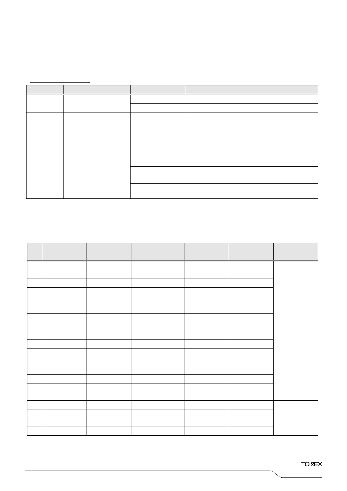
■PRODUCT CLASSIFICATION
●Selection Guide
1. EN Input Logic, Internal Pull-up / down as option
SERIES CE INPUT LOGIC
XC6402 * A ~ D High Active with pull-down resistance
XC6402 * E ~ K High Active with no pull-down resistance
XC6402 * L ~ P Low Active with pull-up resistance
XC6402 * R ~ U Low Active with no pull-up resistance
2. VD Sense as option
SERIES VD SENSE PIN
XC6402 * A, B, E, F, L, M, R, S, V, X VIN
XC6402 * C, D, H, K, N, P, T, U, Y, Z VROUT
3. VD Output Logic as option
SERIES VD OUTPUT LOGIC
XC6402 * A, C, E, H, L, N, R, T, V, Y Detect L
XC6402 * B, D, F, K, M, P, S, U, X, Z Detect H
PIN NAME FUNCTION
USP-6B (BOTTOM VIEW)
*The dissipation pad for the USP-6B package
should be solder-plated in recommended mount
pattern and metal masking so as to enhance
mounting strength and heat release.
If the pad needs to be connected to other pins, it
should be connected to the V
SS pin.
2/31
r
■PRODUCT CLASSIFICATION (Continued)
●Ordering Information
XC6402 ①②③④⑤⑥-⑦
(*1)
DESIGNA TOR DESCRIPTION SYMBOL DESCRIPTION
①
Operational Function
C EN function
F Cd Pin
②
Type of Regulator - As in the chart below
Internally set sequential number relating to output
voltage and detect voltage.
VR setting output voltage range: 0.8V ~ 5.0V
Detect voltage setting range: 0.8V ~ 5.0V
③ ④
Output Voltage & Detect
Voltage
-
50mV increments are available
MR SOT-25
MR-G SOT-25
PR SOT-89-5
⑤⑥-⑦
Packages
Taping Type
(*2)
PR-G SOT-89-5
DR USP-6B
(*1)
The “-G” suffix indicates that the products are Halogen and Antimony free as well as being fully RoHS compliant.
(*2)
The device orientation is fixed in its embossed tape pocket. For reverse orientation, please contact your local Tore x sales office o
representative. (Standard orientation: ⑤R-⑦, Reverse orientation: ⑤L-⑦)
PIN NUMBER : ② Types
EN FUNCTION EN LOGIC
②
PULL UP/DOWN
RESISTANCE
VD SENSE PIN
VD OUTPUT
LOGIC
PIN NUMBER ①
XC6402
Series
A
B
C
D
E
F
H
K
L
M
N
P
R
S
T
U
V
X
Y
Z
Functional High Active Pull-down Function V
Functional High Active Pull-down Function V
Functional High Active Pull-down Function V
Functional High Active Pull-down Function V
Functional High Active Nonfunctional V
Functional High Active Nonfunctional V
Functional High Active Nonfunctional V
Functional High Active Nonfunctional V
Functional Low Active Pull-up Function V
Functional Low Active Pull-up Function V
Functional Low Active Pull-up Function V
Functional Low Active Pull-up Function V
Functional Low Active Nonfunctional V
Functional Low Active Nonfunctional V
Functional Low Active Nonfunctional V
Functional Low Active Nonfunctional V
Nonfunctional - - V
Nonfunctional - - V
Nonfunctional - - V
Nonfunctional - - V
IN Detect L
IN Detect H
ROUT Detect L
ROUT Detect H
IN Detect L
IN Detect H
ROUT Detect L
ROUT Detect H
IN Detect L
IN Detect H
ROUT Detect L
ROUT Detect H
IN Detect L
IN Detect H
ROUT Detect L
ROUT Detect H
IN Detect L
IN Detect H
ROUT Detect L
ROUT Detect H
C Series
F Series
3/31
XC6402 Series
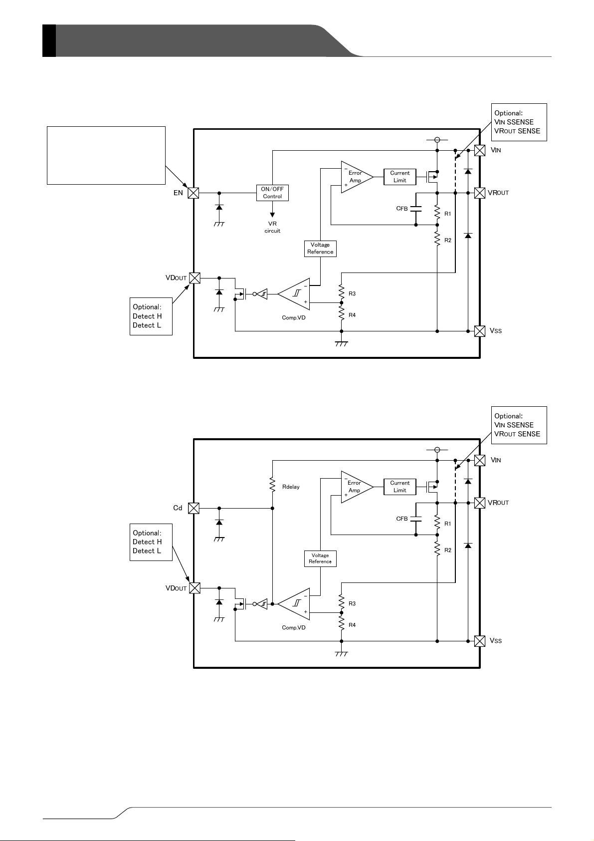
■BLOCK DIAGRAMS
Optional:
High Active with pull-down R
High Active with no pull-down R
Low Active with pull-up R
Low Active with no pull-up R
* Diodes inside the circuit are an ESD protection diode and a parasitic diode.
XC6402C Series
XC6402F Series
4/31

A
■
BSOLUTE MAXIMUM RATINGS
PARAMETER SYMBOL RATINGS UNITS
Input Voltage VIN 6.5 V
VR Output Current IROUT 800 mA
VR Output Voltage VROUT VSS -0.3 ~ VIN +0.3 V
VD Output Current IDOUT 50 mA
VD Output Voltage VDOUT VSS -0.3 ~ 6.5 V
EN / Cd Pin Voltage VEN / Cd VSS -0.3 ~ 6.5 V
SOT-25 250
Power Dissipation
SOT-89-5 500
Pd
USP-6B
Operating Temperature Range Topr - 40 ~ + 85
Storage Temperature Range Tstg - 55 ~ + 125
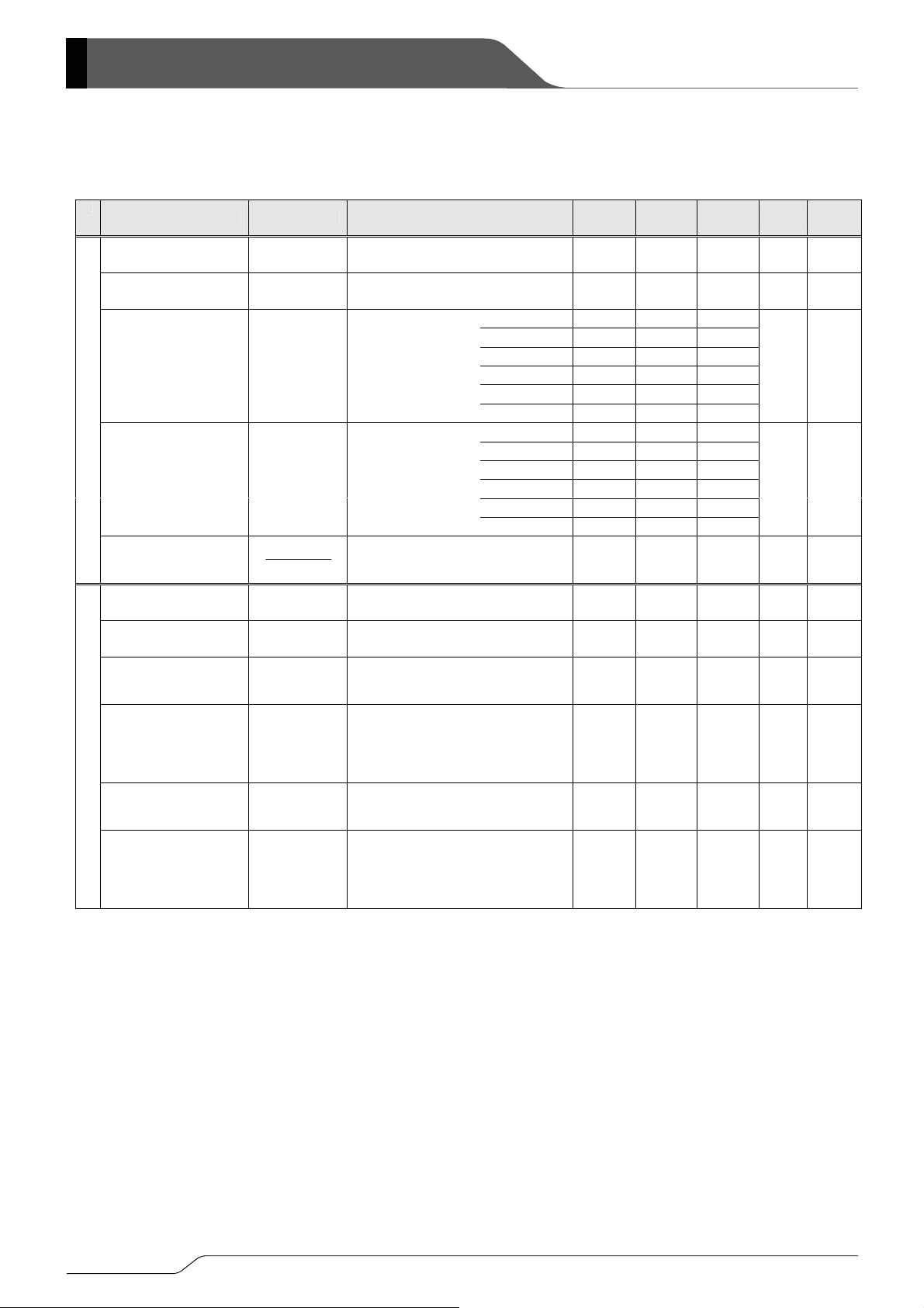
■ELECTRICAL CHARACTERISTICS
XC6402C Series
PARAMETER SYMBOL CONDITIONS MIN. TYP. MAX. UNITS CIRCUIT
100
Ta = 25℃
mW
℃
℃
XC6402
Series
Ta=25℃
Output Voltage
(*2, 3)
Maximum Output
Current
[VROUT(E)≧1.6V]
Maximum Output
Current
[VROUT(E)<1.6V]
VROUT(E) VIN=VROUT(T)+1.0V, IROUT=30mA
IROUTMAX
IROUTMAX
VIN=VROUT(T)+1.0V
VEN=ON(VIN or VSS)
VIN=VROUT(T)+1.0V
VEN=ON(VIN or VSS)
×0.98
(-30m)
VROUT(T)
×1.02
(+30mV)
V ①
700 - - mA ①
500 - - mA ①
Load Regulation △VROUT 1mA≦IROUT≦100mA - 15 60 mV ①
Vdif1 IROUT=30mA E-1
Dropout Voltage (*4)
Supply Current
(CA/CB/CC/CD type)
Supply Current
(CL/CM/CN/CP type)
Supply Current
(CE/CF/CH/CK type)
Supply Current
(CR/CS/CT/CU type)
Line Regulation
VOLTAGE REGULATOR
Vdif2 I
IDD
IDD
IDD
IDD
△VROUT
△VIN・VROUT
ROUT=100mA E-2
VEN=VIN=VROUT(T)+1.0V,
IROUT=0mA
VIN=VROUT(T)+1.0V, VEN=VSS,
IROUT=0mA
VEN=VIN=VROUT(T)+1.0V,
IROUT=0mA
VIN=VROUT(T)+1.0V, VEN=VSS,
IROUT=0mA
VROUT(T)+1.0V≦VIN≦6.0V
VEN=ON(VIN or VSS),
I
ROUT=30mA
E-3 μA ②
E-3 μA ②
- 35 70 μA ②
- 35 70 μA ②
- 0.01 0.20 %/V ①
mV ①
Input Voltage VIN 1.5 - 6.0 V -
Output Voltage
Temperature
Characteristics
△VROUT
△Topr・VROUT
IROUT=30mA
-40℃≦Topr≦85℃
- ±100 -
ppm
/ ℃
①
VIN=[VROUT(T)+1.0]VDC+0.5Vp-pAC
Ripple Rejection
Rate
PSRR
When VROUT(T)≧4.75V
→ VIN=5.75V+0.5Vp-pAC
- 60 - dB ③
IROUT=30mA, f=1kHz
Current Limiter
[VROUT(E)≧1.6V]
Current Limiter
[VROUT(E)<1.6V]
IRlim
IRlim
Short-Circuit Current IRshort
VIN= VROUT(T)+1.0V
VEN=ON(VIN or VSS)
VIN= VROUT(T)+1.0V
VEN=ON(VIN or VSS)
VIN= VROUT(T)+1.0V
VEN=ON(VIN or VSS)
700 800 - mA ①
- 800 - mA ①
- 30 - mA ①
5/31
XC6402 Series
■ELECTRICAL CHARACTERISTICS (Continued)
XC6402C Series (Continued)
PARAMETER SYMBOL CONDITIONS MIN. TYP. MAX. UNITS CIRCUIT
Ta=25℃
Detect Voltage
(*7, 8)
Hysteresis Range
(*7)
V
DF(E)
HYS
V
×0.98
(-30mV)
V
DF(E)
×0.02
VDF(T)
V
DF(E)
×0.05
×1.02
(+30mV)
VDF(E)
×0.08
VIN = 1.5V - 5.0 14.0
VIN = 2.0V - 5.5 14.5
Supply Current IDDVD
EN = OFF
V
(V
IN or VSS)
VIN = 3.0V - 6.0 15.0
VIN = 4.0V - 6.5 15.5
μA ②
VIN = 5.0V - 7.0 16.0
V
IN = 6.0V - 7.5 17.0
VIN = 1.5V 1.5 3.0 VIN = 2.0V 1.8 3.5 -
Output Current
VOLTAGE DETECTOR
(*9)
I
DOUT VDOUT = 0.5V
VIN = 3.0V 1.8 3.7 VIN = 4.0V 1.9 3.8 -
mA ⑤
VIN = 5.0V 1.9 3.9 V
IN = 6.0V 2.0 4.0 -
Detect Voltage
Temperature
Characteristics
EN "High" Level
Voltage
EN "Low" Level
Voltage
△V
DF /
△Topr ・ V
DF
V
ENH 1.30 - VIN V ①
V
ENL - - 0.25 V ①
-40℃≦Topr≦85℃ - ±100 -
ppm
/ ℃
EN "High" Level
ENH VEN=VIN=VROUT(T)+1.0V -0.10 - E-4 μA ①
Current
I
(CA/CB/CC/CD type)
EN "High" Level
Current
I
(CE/CF/CH/CK/CL/
CM/CN/CP/CR/CS/
SWITCH
CT/CU type)
ENH -0.10 - 0.10 μA ①
EN "High" Level
ENL VIN=VROUT(T)+1.0V, VEN=VSS E-5 - 0.10 μA ①
Current
I
(CL/CM/CN/CP type)
EN "High" Level
Current
I
(CA/CB/CC/CD/CE/
ENL VIN=VROUT(T)+1.0V, VEN=VSS -0.10 - 0.10 μA ①
CF/CH/CK/CR/CS/
CT/CU type)
NOTE:
*1: Unless otherwise stated, V
*2: V
ROUT(T)=Specified VR output voltage
*3: V
ROUT(E)=Effective VR output voltage.
(i.e. the VR output voltage when "V
*4: Vdif={V
*5: A voltage equal to 9 8% o f th e VR o u tp u t vo ltage when e v er a s t a b i li ze d V
*6: V
IN1=The input voltage when VOUT1, which appears as input voltage is gradually decreased.
*7: V
DF(T) : Specified detect voltage value
*8: V
DF(E) : Effective detect voltage value.
*9: VD output current value of detect 'L' type equal to current value during detection and that of Detect 'H' type equal to current value before
detection.
*10: V
ROUT(T)≦1.45V, VDF(T)≦1.45V → MIN : VROUT(T) -30mV, VDF(T) -30mV,
→ MAX : V
*11: EN conditions: XC6402CZ / CB / CC / CD / CE / CF / CH / CK type: ON=V
XC6402CL / CM / CN / CP / CR / CS / CT / CU type: ON=V
*12: VD detect voltage: For V
IN1
(*6)
- VROUT1
IN=VROUT(T)+1.0V
(*5)
}
ROUT(T)+1.0V" is provided at the VIN pin while main t ain ing a cer t ai n IROUT value).
ROUT1=IROUT{VROUT(T)+1.0V} is input.
ROUT(T) +30mV, VDF(T) +30mV
IN, OFF=VSS
SS, OFF=VIN
IN sense version, XC6402CA / CB / CE / CF / CL / CM / CR / CS, only VDF(T)≧1.5V type are available.
V ④
V ④
④
6/31
■ELECTRICAL CHARACTERISTICS (Continued)
XC6402F Series
PARAMETER SYMBOL CONDITIONS MIN. TYP. MAX. UNITS CIRCUIT
Output Voltage
(*2, 3)
V
ROUT(E) VIN=VROUT(T)+1.0V, IROUT=30mA
Maximum Output
Current
[V
ROUT(E)≧1.6V]
IROUTMAX VIN= VROUT(T)+1.0V 700 - - mA ①
Maximum Output
Current
ROUTMAX VIN= VROUT(T)+1.0V 500 - - mA ①
I
[VROUT(E)<1.6V]
Load Regulation △VROUT 1mA≦IROUT≦100mA - 15 60 mV ①
×0.98
(-30mV)
VROUT(T)
×1.02
(+30mV)
XC6402
Series
Ta=25℃
V ①
Dropout Voltage
(*4)
Vdif1 IROUT =30mA E-1
Vdif2 I
ROUT =100mA E-2
Supply Current I DD VIN= VROUT(T)+1.0V - 35 70 μA ②
Line Regulation
△V
IN・VROUT
△V
ROUT
V
ROUT(T)+1.0V≦VIN≦6.0V
ROUT=30mA
I
- 0.01 0.20
Input Voltage VIN 1.5 - 6.0 V -
VOLTAGE REGULATOR
Output Voltage
Temperature
Characteristics
Ripple Rejection
Rate
Current Limiter
[V
ROUT(E)≧1.6V]
Current Limiter
ROUT(E)<1.6V]
[V
△VROUT
・VROUT
△Topr
PSRR
V
IN=[VROUT(T)+1.0]VDC+0.5Vp-pAC
ROUT=30mA
I
-40℃≦Topr≦85℃
When VROUT(T)≧4.75V
IN=5.75V+0.5Vp-pAC
→ V
I
ROUT=30mA, f=1kHz
- ±100 -
- 60 - dB ③
IRlim VIN=VROUT(T)+1.0V 700 800 - mA ①
Rlim VIN=VROUT(T)+1.0V - 800 - mA ①
I
Short-Circuit Current IRshort VIN=VROUT(T)+1.0V - 30 - mA ①
Detect Voltage
(*7, 8)
Hysteresis Range
(*7)
V
DF(E)
HYS
V
×0.98
(-30mV)
DF(E)
V
×0.02
VDF(T)
V
DF(E)
×0.05
×1.02
(+30mV)
VDF(E)
×0.08
VIN = 1.5V 1.5 3.0 VIN = 2.0V 1.8 3.5 -
Output Current
(*9)
I
DOUT VDOUT=0.5V
VIN = 3.0V 1.8 3.7 VIN = 4.0V 1.9 3.8 VIN = 5.0V 1.9 3.9 V
IN = 6.0V 2.0 4.0 -
Detect Voltage
VOLTAGE DETECTOR
Temperature
△VDF /
△Topr ・ V
DF -40℃≦Topr≦85℃ - ±100 -
Characteristics
Delay Resistance Rdelay VIN=6.0V, VCD=0V 1.0 2.0 3.5 MΩ ⑥
NOTE:
*1: Unless otherwise stated, V
*2: V
→ MAX: V
ROUT(T)=Specified VR output voltage
*3: V
ROUT(E)=Effective VR output voltage.
(i.e. the VR output voltage when "V
*4: Vdif={V
*5: A volt ag e equa l to 98% of the VR outp ut vo lt ag e whenev er a st a bilize d V
*6: V
IN1=The input voltage when VOUT1, which appears as input voltage is gradually decreased.
*7: V
DF(T) : Specified detect voltage value
*8: V
DF(E) : Effective detect voltage value.
*9: VD output current value of Detect 'L' type equal to current value during detection
and that of Detect 'H' type equal to current value before detection.
*10: V
ROUT(T)≦1.45V, VDF(T)≦1.45V → MIN: VROUT(T) -30mV, VDF(T) -30mV,
*11: VD detect voltage: For VIN Sense version, XC6402FV / FX, only VDF(T)>1.5V type are available.
IN1
(*6)
- VROUT1
IN=VROUT(T)+1.0V
(*5)
}
ROUT(T)+1.0V" is provided at the VIN pin while maintaining a certain IROUT value).
ROUT1=IROUT{VROUT(T)+1.0V} is input.
ROUT(T) +30mV, VDF(T) +30mV
mV ①
% /
V
ppm
/ ℃
V ④
V ④
mA ⑤
ppm
/ ℃
①
①
④
7/31

XC6402 Series
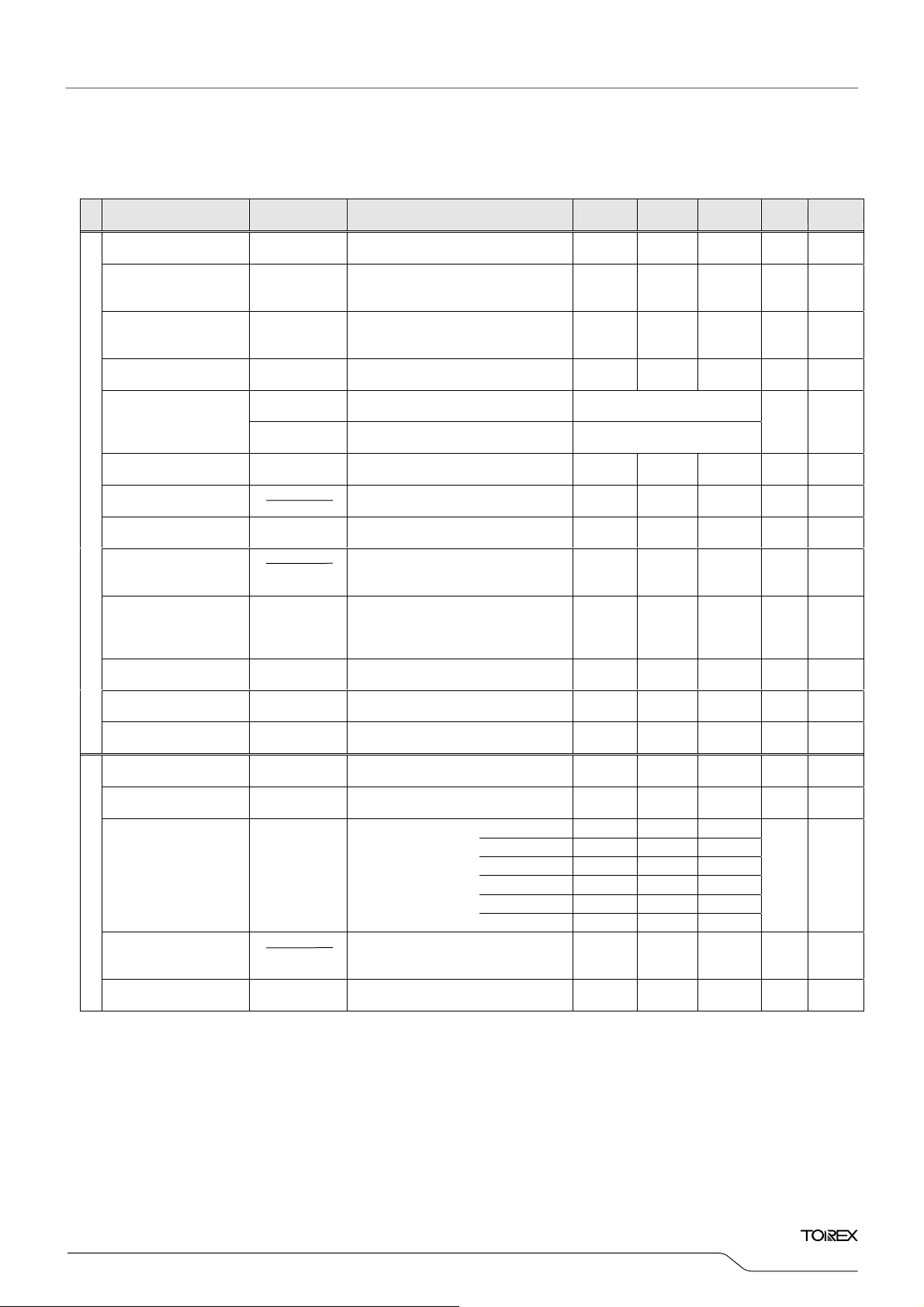
■ELECTRICAL CHARACTERISTICS (Continued)
●Dropout Voltage, Supply Current, EN’H/L’ Level Current
XC6402C Series
SETTING
OUTPUT
VOLTAGE
(V)
VROUT(T) MIN. MAX. TYP. MAX. TYP. MAX. TYP. MAX. MAX. MIN.
0.80 0.770 0.830
0.85 0.820 0.880
0.90 0.870 0.930
0.95 0.920 0.980
1.00 0.970 1.030
1.05 1.020 1.080
1.10 1.070 1.130
1.15 1.120 1.180
1.20 1.170 1.230
1.25 1.220 1.280
1.30 1.270 1.330
1.35 1.320 1.380
1.40 1.370 1.430
1.45 1.420 1.480
1.50 1.470 1.530
1.55 1.519 1.581
1.60 1.568 1.632
1.65 1.617 1.683
1.70 1.666 1.734
1.75 1.715 1.785
1.80 1.764 1.836
1.85 1.813 1.887
1.90 1.862 1.938
1.95 1.911 1.989
2.00 1.960 2.040
2.05 2.009 2.091
2.10 2.058 2.142
2.15 2.107 2.193
2.20 2.156 2.244
2.25 2.205 2.295
2.30 2.254 2.346
2.35 2.303 2.397
2.40 2.352 2.448
2.45 2.401 2.499
2.50 2.450 2.550
2.55 2.499 2.601
2.60 2.548 2.652
2.65 2.597 2.703
2.70 2.646 2.754
2.75 2.695 2.805
2.80 2.744 2.856
2.85 2.793 2.907
2.90 2.842 2.958
2.95 2.891 3.009
VD DETECT VOLTAGE
(V)
VOUT Vdif1 Vdif2 IDD IENH IENL
DROPOUT VOLT AGE 1
E-1 E-2 E-3 E-4 E-5 VR OUTPUT VOLTAGE
DROPOUT VOLT AGE 2
(mV)
700 800
100
600
500 600
50
400
300 400
30
27.0 41.0 90.0 135.0 39.0 83.0 8.0 -8.0
25.0 37.0 80.0 120.0 39.5 84.5 9.5 -9.5
18.0 28.0 60.0 90.0 40.0 86.0 11.0 -11.0
200 300
100
250
150
100
(mV)
700
500
250
SUPPLY CURRENT
(μA)
38.0 80.0 5.0 -5.0
38.5 81.5 6.5 -6.5
EN'H'LEVEL
CURRENT (μA)
EN'H'LEVEL
CURRENT (μA)
8/31

■ELECTRICAL CHARACTERISTICS (Continued)
●Dropout Voltage, Supply Current, EN’H/L’ Level Current (Continued)
XC6402C Series (Continued)
SETTING
OUTPUT
VOLTAGE
VROUT(T) MIN. MAX. TYP. MAX. TYP. MAX. TYP. MAX. MAX. MIN.
3.00 2.940 3.060
3.05 2.989 3.111
3.10 3.038 3.162
3.15 3.087 3.213
3.20 3.136 3.264
3.25 3.185 3.315
3.30 3.234 3.366
3.35 3.283 3.417
3.40 3.332 3.468
3.45 3.381 3.519
3.50 3.430 3.570
3.55 3.479 3.621
3.60 3.528 3.672
3.65 3.577 3.723
3.70 3.626 3.774
3.75 3.675 3.825
3.80 3.724 3.876
3.85 3.773 3.927
3.90 3.882 3.978
3.95 3.871 4.029
4.00 3.920 4.080
4.05 3.969 4.131
4.10 4.018 4.182
4.15 4.067 4.233
4.20 4.116 4.284
4.25 4.165 4.335
4.30 4.214 4.386
4.35 4.263 4.437
4.40 4.312 4.488
4.45 4.361 4.539
4.50 4.410 4.590
4.55 4.459 4.641
4.60 4.508 4.692
4.65 4.557 4.743
4.70 4.606 4.794
4.75 4.655 4.845
4.80 4.704 4.896
4.85 4.753 4.947
4.90 4.802 4.998
4.95 4.851 5.049
5.00 4.900 5.100
VR OUTPUT VOLTAGE
VD DETECT VOLTAGE
(V)
(V)
VOUT Vdif1 Vdif2 IDD IENH IENL
E-1 E-2 E-3 E-4 E-5
DROPOUT
VOLTAGE 1
(mV)
15.0 23.0 50.0 75.0
DROPOUT
VOLTAGE 2
(mV)
SUPPLY CURRENT
(μA)
40.5 87.5 12.5 -12.5
41.0 89.0 14.0 -14.0
41.5 90.5 15.5 -15.5
42.0 92.0 17.0 -17.0
EN'H'LEVEL
CURRENT
(μA)
EN'H'LEVEL
CURRENT
XC6402
Series
(μA)
9/31

XC6402 Series
■ELECTRICAL CHARACTERISTICS (Continued)
●Dropout Voltage
XC6402F Series
SETTING
OUTPUT
VOLTAGE
VD DETECT VOLTAGE
(V)
(V)
DROPOUT VOLTAGE 1
VOUT Vdif1 Vdif2
VROUT(T) MIN. MAX. TYP. MAX. TYP. MAX.
0.80 0.770 0.830
0.85 0.820 0.880
0.90 0.870 0.930
0.95 0.920 0.980
1.00 0.970 1.030
1.05 1.020 1.080
1.10 1.070 1.130
1.15 1.120 1.180
1.20 1.170 1.230
1.25 1.220 1.280
1.30 1.270 1.330
1.35 1.320 1.380
1.40 1.370 1.430
1.45 1.420 1.480
1.50 1.470 1.530
1.55 1.519 1.581
1.60 1.568 1.632
1.65 1.617 1.683
1.70 1.666 1.734
1.75 1.715 1.785
1.80 1.764 1.836
1.85 1.813 1.887
1.90 1.862 1.938
1.95 1.911 1.989
2.00 1.960 2.040
2.05 2.009 2.091
2.10 2.058 2.142
2.15 2.107 2.193
2.20 2.156 2.244
2.25 2.205 2.295
2.30 2.254 2.346
2.35 2.303 2.397
2.40 2.352 2.448
2.45 2.401 2.499
2.50 2.450 2.550
2.55 2.499 2.601
2.60 2.548 2.652
2.65 2.597 2.703
2.70 2.646 2.754
2.75 2.695 2.805
2.80 2.744 2.856
2.85 2.793 2.907
2.90 2.842 2.958
2.95 2.891 3.009
E-1 E-2 VR OUTPUT VOLTAGE
DROPOUT VOLTAGE 2
(mV)
(mV)
700 800
100
600
250
700
500 600
50
400
150
500
300 400
30
200 300
100
100
250
27.0 41.0 90.0 135.0
25.0 37.0 80.0 120.0
18.0 28.0 60.0 90.0
10/31

■ELECTRICAL CHARACTERISTICS (Continued)
●Dropout Voltage (Continued)
XC6402F Series (Continued)
SETTING
OUTPUT
VOLTAGE
(V)
VD DETECT VOLTAGE
(V)
VOUT Vdif1 Vdif2
DROPOUT VOLTAGE 1
E-1 E-2 VR OUTPUT VOLTAGE
(mV)
DROPOUT VOLTAGE 2
(mV)
VROUT(T) MIN. MAX. TYP. MAX. TYP. MAX.
3.00 2.940 3.060
3.05 2.989 3.111
3.10 3.038 3.162
3.15 3.087 3.213
3.20 3.136 3.264
3.25 3.185 3.315
3.30 3.234 3.366
3.35 3.283 3.417
3.40 3.332 3.468
3.45 3.381 3.159
3.50 3.430 3.570
3.55 3.479 3.621
3.60 3.528 3.672
3.65 3.577 3.723
3.70 3.626 3.774
3.75 3.675 3.825
3.80 3.724 3.876
3.85 3.773 3.927
3.90 3.882 3.978
3.95 3.871 4.029
4.00 3.920 4.080
15.0 23.0 50.0 75.0
4.05 3.969 4.131
4.10 4.018 4.182
4.15 4.067 4.233
4.20 4.116 4.284
4.25 4.165 4.335
4.30 4.214 4.386
4.35 4.263 4.437
4.40 4.312 4.488
4.45 4.361 4.539
4.50 4.410 4.590
4.55 4.459 4.641
4.60 4.508 4.692
4.65 4.557 4.743
4.70 4.606 4.794
4.75 4.655 4.845
4.80 4.704 4.896
4.85 4.753 4.947
4.90 4.802 4.998
4.95 4.851 5.049
5.00 4.900 5.100
XC6402
Series
11/31

XC6402 Series
■TEST CIRCUITS
XC6402C Series
Circuit ① Circuit ②
Circuit ③
Circuit ④
Circuit ⑤
Output Capacitor Corresponding Chart
VR OUTPUT VOLTAGE 0.8 ~1.45V 1.5 ~ 1.75V 1.8V ~ 5.0V
XC6402CA / CB / CE / CF/ CL / CM / CS type XC6402 CC / CD / CH / CK / CN / CP / CT / CU type
220kΩ
XC6402CA / CB / CE / CF/ CL / CM / CS type
CL
6.8μF 2.2μF 1.0μF
XC6402 CC / CD / CH / CK / CN / CP / CT / CU type
220kΩ
12/31

■TEST CIRCUITS (Continued)
XC6402F Series
Circuit ① Circuit ②
Circuit ③
Circuit ④
Circuit ⑤
Circuit ⑥
Output Capacitor Corresponding Chart
XC6402FY / FX type
XC6402FY / FX type
XC6402FY / FX type
220kΩ
XC6402FY / FZ type
XC6402FY / FZ type
XC6402FY / FZ type
VR OUTPUT VOLTAGE 0.8 ~1.45V 1.5 ~ 1.75V 1.8V ~ 5.0V
CL
6.8μF 2.2μF 1.0μF
XC6402
Series
220kΩ
13/31

XC6402 Series
■OPERATIONAL EXPLANATION
<Output Voltage Regulator Control>
The voltage, divided by resistors R1 & R2 which are conne cted to the V
voltage by the error amplifier. The P-channel MOSFET, which is connected to the V
subsequent output signal. The output voltage at the V
limit circuit and short circuit protection operate in relation to the level of output current. Further, the voltage regulator's
internal circuitry can be shutdown via the EN pin's signal.
<Detector Function with the XC6402 Series>
The series' detector function monitors the voltage divided by resistors R3 & R4 which are connected to the V
V
IN pin, as well as monitoring the voltage of the internal reference voltage source via the comparator.
The V
DSEN pin has options (please refer to the Selection Guide, item 2).
A 'High' or 'Low' signal level can be output from the V
The VD output logic has options (please refer to the Selection Guide, item 3). As V
output, a pull-up resistor of about 220kΩ is neede d to achieve a voltage output. Because of hysteresis at the detector
function, output at the V
DOUT pin will invert when the detect voltage level increases above the release voltage (105% of the
detect voltage).
For the XC6402C type, in stand-by, if a voltage of the recovery voltage is present at the V
source), the V
DOUT pin will be high impedance mode, and the pu ll up voltage will be output at VDOUT. By connecting the
Cdelay pin to a capacitor (Cd), the XC6402F series can apply a delay time to V
delay time can be calculated from the internal resistance, Rdelay (2MΩ TYP. fixed) and the value of Cd as per the following
equation.
Delay Time = Cdelay x Rdelay x 0.7
Delay Time
Rdelay standard : 1.0 ~ 3.5MΩ
Cdelay DELAY TIME (TYP.) DELAY TIME
0.01μF
0.022μF
0.047μF
0.1μF
0.22μF
0.47μF
1μF
<Low ESR Capacitors>
With the XC6402 series regulator, a stable output voltage is achievable even if low ESR capacitors are used, as a phase
compensation circuit is built-in to the regulator. In order to ensure the effectiveness of the phase compensation, we suggest
that an output capacitor (CL) be connected as close as possible, between the output pin (V
an output capacito r (CL) with a ca pacitance, based o n the chart below. We also suggest an input capacitor (CIN) of 1μF :
this should be connected between VIN and VSS in order to stabilize input power source.
Output Capacitor Corresponding Chart
VR OUTPUT VOLTAGE 0.8 ~1.45V 1.5 ~ 1.75V 1.8V ~ 5.0V
CL
<Current Limiter, Short-Circuit Protection>
The XC6402 series regulator offers a combination of current limit and circuit protection by means of a built-in fixed current limiter
ROUT pin is controlled & stabilized by negative feedback. T he current
DOUT pin when the VD pin voltage level goes below the detect voltage.
14 ms 7.0 ~ 24.5 ms
30.8 ms 15.4 ~ 53.9 ms
65.8 ms 32.9 ~ 115.15 ms
140 ms 70.0 ~ 245.0 ms
308 ms 154.0 ~ 539.0 ms
658 ms 329.0 ~ 1151.5 ms
1400 ms 700.0 ~ 2450.0 ms
6.8μF 2.2μF 1.0μF
circuit and a foldback circuit. When the load current reaches t he current limit level, the f ixed current limiter circuit operates and
output voltage drops. As a result of this drop in output voltage, the foldback circuit operates, the output voltage drops further and
output current decreases. When the output pin is shorted, a current of about 30mA flow s.
ROUT pin is compared with the internal reference
ROUT pin, is then driven by the
ROUT pin or the
DOUT is an open-drain N-channel
ROUT pin (from another power
DOUT voltage when releasing voltage. T he
TYP : 2.0MΩ
ROUT) and the VSS pin. Please use
14/31

XC6402
■OPERATIONAL EXPLANATION (Continued)
<EN Pin>
The IC's internal regulator circuitry can be shut down via the signal from the EN pin with the XC6402C series. In shutdown
mode, output at the V
the XC6402C series are 'High Active / No Pull-Down' and XC6402*R to U types of the XC6402C series are 'Active LOW / No
Pull-Up', operations will become unstable with the EN pin open (See the chart below).
We suggest that you use this IC with either a V
correct specifications for the EN pin, the IC will operate normally. Ho wever, supply current may increase as a result of
through current in the IC's internal circuitry if a voltage other than VIN or VSS is applied.
■NOTES ON USE
1. Please use this IC within the stated absolute maximum ratings. The IC is liable to malfunction should the ratin gs be
exceeded.
2. Where wiring impedance is high, operations may become unstable due to noise and/or phase lag depen ding on output
current. Please strengthen V
3. Please wire the input capacitor (C
Should rapid input fluctuation or load fluctuation o ccur, please increase the capacitor value such as C
the operation.
ROUT pin will be pulled down to the VSS level via R1 & R2. Note that as the XC6402*E to K types of
SERIES EN INPUT LOGIC
XC6402C A ~ D High Active with pull-down resistor
XC6402C E ~ K High Active with no pull-down resistor
XC6402C L ~ P Low Active with pull-up resistor
XC6402C R ~ U Low Active with no pull-up resistor
IN voltage or a VSS voltage input at the EN pin. If this IC is used with the
IN and VSS wiring in particular.
IN) and the output capacitor (CL) as close to the IC as possible.
IN or CL to stabilize
Series
15/31

XC6402 Series
■TYPICAL PERFORMANCE CHARACTERISTICS
(1) VR Output Voltage vs. VR Output Current
0.9
0.8
0.7
0.6
0.5
0.4
0.3
Output Volt age VR OUT(V)
0.2
0.1
0
0 100 200 300 400 500 600 700 800 900
4.0
3.5
3.0
2.5
2.0
1.5
Output Voltage VR OU T(V)
1.0
0.5
0.0
0 100 200 300 400 500 600 700 800 900
6.0
5.0
4.0
3.0
2.0
Output Volt age VROU T (V)
1.0
0.0
0 100 200 300 400 500 600 700 800 900
XC6402 Series (VR: 0.8V)
XC6402 Seri es (VR :0. 8V)
VIN=1.8V, CIN=1.0μF(ceramic),CL=6.8μF(ceramic)
Topr= - 40
℃
Topr= 25
℃
Topr= 85
℃
VR Out put Current I R OUT(mA)
XC6402 Ser ies (VR :3. 0V)
VIN =4.0V, CIN =1.0μF(ceramic),CL=1.0μF(ceramic)
Topr= - 40
℃
Topr= 25
℃
Topr= 85
℃
VR Out put C urrent I ROU T(mA)
XC6402 Series (VR: 5.0V)
XC6402 Series (VR : 5.0V) XC6402 Series (VR: 5.0V)
XC6402 Ser i es (VR :5. 0V)
VIN =6.0V, CIN =1.0μF(ceramic),CL=1.0μF(ceramic)
Topr= - 40
℃
Topr= 25
℃
Topr= 85
℃
VR Out put C urrent I R OU T(mA)
XC6402 Series (VR: 0.8V)
XC6402 Series (VR: 3.0V) XC6402 Series (VR: 3.0V)
16/31

■TYPICAL PERFORMANCE CHARACTERISTICS (Continued)
(2) VR Output Voltage vs. Input Voltage
1.1
XC6402 Series (VR: 0.8V)
XC6402 Ser ies (VR :0. 8V)
Topr=25℃, CIN=1.0μF(ceramic),CL=6.8μF(ceramic)
XC6402 Series (VR: 0.8V)
1.0
0.9
0.8
0.7
Output Volt age VR OU T (V)
0.6
IOUT=0mA
IOUT=30mA
IOUT=100mA
0.5
0.5 1.0 1.5 2.0 2.5
Input Volt age VI N (V)
3.2
Topr=25℃, CIN=1.0μF(ceramic),CL=1.0μF(ceramic)
XC6402 Series (VR :3.0V)
XC6402 Series (VR: 3.0V)
XC6402 Series (VR: 3.0V)
3.0
2.8
2.6
Output Volt age VR OU T (V)
2.4
IOUT=0mA
IOUT=30mA
IOUT=100mA
IOUT=500mA
2.2
2.5 3.0 3.5
Input Volt age VI N (V)
XC6402 Series (VR: 5.0V)
XC6402 Series (VR: 5.0V)
XC6402
Series
17/31

XC6402 Series
■TYPICAL PERFORMANCE CHARACTERISTICS (Continued)
(3) Dropout Voltage vs. Output Current
1.0
0.8
0.6
0.4
Dropout Volt a ge Vdif (V)
0.2
0.0
0 100 200 300 400 500
0.6
0.5
0.4
0.3
0.2
Dropout Volt age Vdif (V)
0.1
0.0
0 100 200 300 400 500
0.6
0.5
0.4
0.3
0.2
Dropout Volt age Vdif (V)
0.1
XC6402 Series (VR: 0.8V)
XC6402 Ser i es (VR :0. 8V)
CIN=1.0μF(ceramic),CL=6.8μF(ceramic)
Topr= - 40
℃
Topr= 25
℃
Topr= 85
℃
VR Out put C urrent I R OU T(m A)
XC6402 Series (VR: 1.5V)
XC6402 Ser i es (VR :1 .5 V)
CIN=1.0μF(ceramic),CL=2.2μF(ceramic)
Topr= - 40
℃
Topr= 25
℃
Topr= 85
℃
VR Out put C urrent I R OUT(mA)
XC6402 Ser i es (VR :3. 0V)
XC6402 Series (VR: 3.0V)
CIN=1.0μF(ceramic),CL=1.0μF(ceramic)
Topr= - 40
℃
Topr= 25
℃
Topr= 85
℃
XC6402 Series (VR: 1.2V)
XC6402 Ser i es (VR :1. 2V)
0.8
0.7
0.6
0.5
0.4
0.3
Dropout Volt age Vdif(V)
0.2
0.1
0.0
0 100 200 300 400 500
0.6
0.5
0.4
0.3
0.2
Dropout Volt age Vdif (V )
0.1
0.0
0 100 200 300 400 500
0.6
0.5
0.4
0.3
0.2
Dropout Volt age Vdif (V)
0.1
CIN=1.0μF(ceramic),CL=6.8μF(ceramic)
Topr= - 40
℃
Topr= 25
℃
Topr= 85
℃
VR Output Current IROUT(mA)
XC6402 Ser i es (VR :2. 5 V)
XC6402 Series (VR: 2.5V)
CIN=1.0μF(ceramic),CL=1.0μF(ceramic)
Topr= - 40
℃
Topr= 25
℃
Topr= 85
℃
VR Output Current IROUT(mA)
XC6402 Series (VR: 5.0V)
XC6402 Ser i es (VR :5. 0V )
CIN=1.0μF(ceramic),CL=1.0μF(ceramic)
Topr= - 40
℃
Topr= 25
℃
Topr= 85
℃
0.0
18/31
0 100 200 300 400 500 600 700
VR Out put C urrent I R OU T(mA)
0.0
0 100 200 300 400 500 600 700
VR Output Current IROUT(mA)

■TYPICAL PERFORMANCE CHARACTERISTICS (Continued)
(4) Supply Current vs. Input Voltage
100
XC6402 Ser i es (VR :0. 8V)
XC6402 Series (VR: 0.8V)
CIN=1.0μF(ceramic),CL=6.8μF(ceramic)
100
XC6402 Series (VR: 3.0V)
XC6402 Ser i es (VR :3. 0V )
CIN=1.0μF(ceramic),CL=1.0μF(ceramic)
80
A)
μ
60
Topr= - 40
Topr= 25
Topr= 85
℃
℃
℃
80
A)
μ
60
40
40
Supply C urrent I D D (
20
Supply Current IDD(
20
0
0123456
120
100
A)
80
μ
Input Volt age VI N (V)
XC6402 Ser i es (VR :5 . 0V)
XC6402 Series (VR: 5.0V)
CIN=1.0μF(ceramic),CL=1.0μF(ceramic)
Topr= - 40
℃
Topr= 25
℃
Topr= 85
℃
(5) VR Output Voltage vs. Operating Temperature
0
0123456
Input Volt age VI N (V)
XC6402 Series (VR: 0.8V)
60
40
Supply Current IDD(
20
0
0123456
Input Voltage VIN(V)
XC6402 Series (VR: 5.0V)
XC6402 Series (VR: 3.0V)
XC6402 Series (VR : 5.0V)
XC6402
Top r = - 4 0
Top r = 2 5
Top r = 8 5
Series
℃
℃
℃
19/31

XC6402 Series
■TYPICAL PERFORMANCE CHARACTERISTICS (Continued)
(6) Supply Current vs. Operating Temperature
XC6402 Series (VR: 0.8V)
50
XC6402 Ser i es (VR :0. 8V )
VIN =1.8V, CIN =1.0μF(ceramic),CL=6.8μF(ceramic)
45
A)
μ
40
35
Supply C urrent I D D (
30
25
-50-25 0 25 50 75100
Operating Temperat ur e Topr(℃)
50
XC6402 Series (VR: 5.0V)
XC6402 Ser ies (VR :5. 0V)
VIN=6.0V, CIN=1.0μF(ceramic),CL=1.0μF(ceramic)
45
A)
μ
40
35
Supply Current IDD(
30
25
-50 -25 0 25 50 75 100
(8) Rdelay vs. Operating Temperature (For F Series only)
4.0
3.5
Operating Temperat ure Topr(℃)
XC6402F Ser i es
XC6402F Series
3.0
2.5
)
Ω
2.0
Rdelay (M
1.5
1.0
0.5
0.0
-50 -25 0 25 50 75 100
Operating Temper at ure Topr(℃)
50
45
A)
μ
40
35
Supply Current IDD(
30
25
-50 -25 0 25 50 75 100
(7) EN Threshold Voltage vs. Operatin g Temperature
(For C Series only)
XC6402 Series (VR: 3.0V)
XC6402 Ser i es (VR :3. 0V )
VIN=4.0V, CIN=1.0μF(ceramic),CL=1.0μF(ceramic)
Operating Temper at ure Topr(℃)
XC6402C Series
20/31

R
■TYPICAL PERFORMANCE CHARACTERISTICS (Continued)
(9) VD Supply Current vs. Input Voltage (For C Series only)
XC6402C Ser i es (VD :0. 8V)
20
XC6402C Series (VD: 0.8V)
20
XC6402C Series (VD: 3.0V)
XC6402C Ser ies (VD :3. 0V)
A)
15
μ
10
Topr= - 40
Topr= 25
Topr= 85
℃
℃
℃
A)
15
μ
10
Topr= - 40
Topr= 25
Topr= 85
℃
℃
℃
5
VD Supply Current IDDVD(
5
VD Supply C urrent I D D V D(
0
0123456
Input Volt age VI N (V)
XC6402C Ser i es (VD :5. 0V)
20
XC6402C Series (VD: 5.0V)
0
0123456
Input Volt age VI N (V)
(10) Detect Voltage & Release Voltage vs.
Operating Temperature
XC6402 Series (VD: 0.8V)
A)
15
μ
10
Topr= - 40
Topr= 25
Topr= 85
℃
℃
℃
5
VD Supply Current IDDVD(
0
0123456
Input Volt age VI N (V)
XC6402 Series (VD: 3.0V)
XC6402 Series (VD: 5.0V)
XC6402
Series
21/31

XC6402 Series
■TYPICAL PERFORMANCE CHARACTERISTICS (Continued)
(11) VD N-ch Driver Tr. Output Current vs. VDS
XC6402 Series (VD)
10
XC6402 Series (VD :3.0V)
XC6402 Series (VD: 3.0V)
8
6
4
Topr= - 40
Topr= 25
Topr= 85
℃
℃
℃
Output Current IDOUT(mA)
2
0
01234
VDS (V)
Input Voltage VIN(V)
VDS=0.5V
(12) VD N-ch Driver T r. Output Current vs. Input Voltage
XC6402 Ser i es (VD :1. 5V)
XC6402 Series (VD : 1.5V)
10
8
6
4
Output C urrent I D OUT(m A)
2
0
00.511.52
10
8
6
4
Output Current IDOUT(mA)
2
0
0123456
Topr= - 40
℃
Topr= 25
℃
Topr= 85
℃
VDS (V)
Input Voltage VIN(V)
XC6402 Ser i es (VD :5. 0V)
XC6402 Series (VR: 5.0V)
Topr= - 40
℃
Topr= 25
℃
Topr= 85
℃
VDS (V)
Input Voltage VIN(V)
VDS=0.5V
VDS=0.5V
22/31

■TYPICAL PERFORMANCE CHARACTERISTICS (Continued)
(13) VR Input Transient Response
1.2
1.1
1.0
0.9
0.8
Output Volt age VR O UT(V)
0.7
0.6
XC6402 Ser i es (VR :0. 8V)
XC6402 Series (VR: 0.8V)
IOU T=30mA, t r=t f =5.0μsec
CL=6.8μF(ceramic),Topr=25
Input Voltage
Output Volt age
Tim e ( 2 0μsec/div)
Time (20μs /div)
XC6402 Series (VR: 0.8V)
XC6402 Ser i es (VR :0. 8V )
℃
4
3
2
1
0
Input Voltage VIN(V)
-1
-2
1.2
1.1
1.0
0.9
0.8
Output Volt age VROU T (V)
0.7
0.6
Time (20μs /div)
IOUT=200mA,tr=tf=5.0μsec
CL=6.8μF(ceramic),Topr=25
Input Volt age
Output Volt age
Tim e ( 2 0μsec/div)
XC6402 Series (VR: 3.0V)
3.4
XC6402 Ser i es (VR :3. 0V)
IOUT=30mA,tr=tf=5.0μsec
CL=1.0μF(ceramic),Topr=25
XC6402 Series (VR: 3.0V)
XC6402 Ser i es (VR :3. 0V )
℃
6
3.4
IOUT=200mA,tr=tf=5.0μsec
CL=1.0μF(ceramic),Topr=25
3.3
5
3.3
3.2
3.1
Input Voltage
4
3
3.2
Input Voltage
3.1
3.0
Output Volt age VR OU T (V)
2.9
Output Volt age
2.8
Tim e ( 2 0μsec/div)
Time (20μs /div)
XC6402 Series (VR: 5.0V)
5.4
XC6402 Series (VR :5.0V)
IOUT=30mA,tr=tf=5.0μsec
CL=1.0μF(ceramic),Topr=25
5.3
2
Input Volt age VI N (V)
1
0
℃
8
7
3.0
Output Vol t age VR O U T (V)
2.9
2.8
5.4
5.3
Output Volt age
Time ( 2 0μsec/div)
Time (20μs /div)
XC6402 Series (VR: 5.0V)
XC6402 Ser ies (VR :5. 0V)
IOUT=200mA,tr=tf=5.0μsec
CL=1.0μF(ceramic),Topr=25
5.2
Input Voltage
6
5.2
Input Voltage
5.1
5
5.1
5.0
Output Volt age VR O UT(V)
4.9
Output Volt age
4
Input Voltage VIN(V)
3
5.0
Output Volt age VR OU T (V)
Output Volt age
4.9
4.8
Tim e ( 2 0μsec/div)
Time (20μs /div)
2
4.8
Time ( 2 0μsec/div)
Time (20μs /div)
XC6402
Series
℃
4
3
2
1
0
Input Volt age VI N (V)
-1
-2
℃
6
5
4
3
2
Input Volt age VI N (V)
1
0
℃
8
7
6
5
4
Input Volt age VIN (V)
3
2
23/31

XC6402 Series
■TYPICAL PERFORMANCE CHARACTERISTICS (Continued)
(14) VR Load Transient Response
XC6402 Series (VR :0.8V)
1.0
XC6402 Series (VR: 0.8V)
VIN=1.8V,tr=tf =5.0μsec,Topr=25
CIN=1.0μF(ceramic),CL=6.8μF(ceramic)
℃
500
1.0
0.8
400
0.8
0.6
Output Volt age
300
0.6
0.4
Output Volt age VR OUT (V)
0.2
100mA
10mA
0.0
Output C urrent
Tim e ( 2 5μsec/div)
Time (25μs /div) Time (25μs /div)
200
Output Current IROUT(mA)
100
0
0.4
200mA
Output Volt age VR O UT(V)
0.2
10mA
0.0
3.4
XC6402 Series (VR :3.0V)
XC6402 Series (VR: 3.0V)
VIN=4.0V,tr=tf =5.0μsec,Topr=25℃,
CIN=1.0μF(ceramic),CL=1.0μF(ceramic)
500
3.4
3.0
400
3.0
2.6
Output Volt age
300
2.6
2.2
Output Volt age VR O UT(V)
1.8
100mA
10mA
1.4
Output C urrent
Tim e ( 2 5μsec/div)
Time (25μs /div)
Time (25μs /div) Time (25μs /div)
200
100
0
2.2
Output C urrent I R OUT (m A)
Output Volt age VR O UT(V)
1.8
10mA
1.4
XC6402 Ser i es (VR :5. 0V)
5.4
5.0
XC6402 Series (VR: 5.0V)
VIN=6.0V,tr=tf=5.0μsec,Topr=25
CIN=1.0μF(ceramic),CL=1.0μF(ceramic)
Output Volt age
℃
500
400
5.4
5.0
4.6
300
4.6
4.2
Output Volt age VR OU T (V)
3.8
3.4
100mA
10mA
Output C urrent
Tim e ( 2 5μsec/div)
Time (25μs /div) Time (25μs /div)
200
Output C urrent I R OU T (m A)
100
0
4.2
200mA
Output Vol t age VR OUT (V)
3.8
3.4
XC6402 Series (VR :0.8V)
XC6402 Series (VR: 0.8V)
VIN=1.8V,tr=tf =5.0μsec,Topr=25
CIN=1.0μF(ceramic),CL=6.8μF(ceramic)
Output Volt age
Output C ur rent
Tim e ( 2 5μsec/div)
XC6402 Series (VR :3.0V)
XC6402 Series (VR: 3.0V)
VIN=4.0V,tr=tf =5.0μsec,Topr=25
CIN=1.0μF(ceramic),CL=1.0μF(ceramic)
Output Volt age
Output Current
200mA
Time ( 2 5μsec/div)
XC6402 Ser i es (VR :5. 0V)
XC6402 Series (VR: 5.0V)
10mA
VIN=6.0V,tr=tf =5.0μsec,Topr=25
CIN=1.0μF(ceramic),CL=1.0μF(ceramic)
Output Volt age
Output Current
Time ( 2 5μsec/div)
℃
500
400
300
200
Output C urrent I R OUT (m A)
100
0
℃
500
400
300
200
Output C urrent I R OUT (m A)
100
0
℃
500
400
300
200
Output Current IROUT(mA)
100
0
24/31

■TYPICAL PERFORMANCE CHARACTERISTICS (Continued)
(15) Ripple Rejection Rate
80
70
60
50
40
30
20
Ripple Rejection Rate RR(dB)
10
0
0.01 0.1 1 10 100
XC6402 Series (VR: 3.0V)
XC6402 Ser i es (VR :3. 0V )
VIN=1.8VDC+0.5Vp-pAC,IOUT=30mA,Topr=25
CIN=1.0μF(ceramic),CL=6.8μF(ceramic)
Ripple F requenc y f (k H z)
XC6402 Ser i es (VR :3. 0V)
℃
80
70
60
50
40
30
20
Ripple Rejection Rate RR(dB)
10
0
0.01 0.1 1 10 100
XC6402 Series (VR: 3.0V)
VIN=4.0VDC+0.5Vp-pAC,IOUT=30mA,Topr=25
CIN=1.0μF(ceramic),CL=1.0μF(ceramic)
Ripple F reque nc y f (k H z)
80
70
60
50
40
30
20
Ripple R ejec t ion R at e R R (dB)
10
XC6402 Series (VR: 3.0V)
XC6402 Series (VR :3.0V)
VIN=5.75VDC+0.5Vp-pAC,IOUT=30mA,Topr=25℃,
CIN=1.0μF(ceramic),CL=1.0μF(ceramic)
0
0.01 0.1 1 10 100
Ripple F requenc y f (k H z)
XC6402
Series
℃
25/31

XC6402 Series
■TYPICAL PERFORMANCE CHARACTERISTICS (Continued)
(16) Rising Response Time
5
4
XC6402 Series (VR: 0.8V)
XC6402 Ser i es (VR :0. 8V)
IOUT=30mA,tr=5.0μsec,Topr=25
CIN=1.0μF(ceramic),CL=6.8μF(ceramic)
Input Volt age
℃
4
2
5
4
3
0
3
2
Output Vol t age VR OUT (V)
1
Output Voltage
-2
Input Volt age VI N (V)
-4
2
Output Volt age VR OUT (V)
1
0
Time ( 2 5μsec/div)
Time (25μs /div) Time (25μs /div)
-6
0
5
4
XC6402 Ser i es (VR :3. 0V)
XC6402 Series (VR: 3.0V)
IOUT=30mA,tr=5.0μsec,Topr=25
CIN=1.0μF(ceramic),CL=1.0μF(ceramic)
Input Volt age
℃
6
4
5
4
3
2
3
2
Output Volt age VR OU T (V)
1
Output Voltage
0
Input Volt age VI N (V)
-2
2
Output Volt age VR OU T (V)
1
0
Time ( 2 5μsec/div)
Time (25μs /div) Time (25μs /div)
-4
0
XC6402 Series (VR: 5.0V)
10
8
XC6402 Ser i es (VR :5. 0V)
IOUT=30mA,tr=5.0μsec,Topr=25
CIN=1.0μF(ceramic),CL=1.0μF(ceramic)
Input Volt age
℃
8
6
10
8
6
4
6
4
Output Voltage
Output Vol t age VR OUT (V)
2
2
Input Volt age VI N (V)
0
4
Output Volt age VR OUT (V)
2
0
Time ( 2 5μsec/div)
Time (25μs /div) Time (25μs /div)
-2
0
XC6402 Series (VR: 0.8V)
XC6402 Ser i es (VR :0. 8V)
IOUT=200mA,tr=5.0μsec,Topr=25
CIN=1.0μF(ceramic),CL=6.8μF(ceramic)
Input Volt age
Output Volt age
Time ( 2 5μsec/div)
XC6402 Series (VR: 3.0V)
XC6402 Ser i es (VR :3. 0V)
IOUT=200mA,tr=5.0μsec,Topr=25
CIN=1.0μF(ceramic),CL=1.0μF(ceramic)
Input Voltage
Output Voltage
Time ( 2 5μsec/div)
XC6402 Ser i es (VR :5. 0V)
XC6402 Series (VR: 5.0V)
IOUT=200mA,tr=5.0μsec,Topr=25
CIN=1.0μF(ceramic),CL=1.0μF(ceramic)
Input Volt age
Output Voltage
Time ( 2 5μsec/div)
℃
4
2
0
-2
Input Volt age VI N (V)
-4
-6
℃
6
4
2
0
Input Volt age VI N (V)
-2
-4
℃
8
6
4
2
Input Volt age VI N (V)
0
-2
26/31

■TYPICAL PERFORMANCE CHARACTERISTICS (Continued)
(17) EN Rising Response Time (For C Series only)
XC6402 Ser i es (VR :0. 8V)
5
4
XC6402 Series (VR: 0.8V)
VIN=1.8V,IOUT=30mA,tr=5.0μsec
CIN=1.0μF(ceramic),CL=6.8μF(ceramic),Topr=25
EN I nput Volt age
℃
4
2
5
4
XC6402 Series (VR: 0.8V)
XC6402 Ser i es (VR :0. 8V )
CIN=1.0μF(ceramic),CL=6.8μF(ceramic),Topr=25
VIN=1.8V,IOUT=30mA,tr=5.0μsec
EN I nput Volt age
3
0
3
2
Output Volt a ge VR OU T(V)
1
Output Volt age
-2
EN I nput V olt age VEN(V)
-4
2
Output Volt age VR OU T (V)
1
Output Voltage
0
CIN=1.0μF(ceramic),CL=1.0μF(ceramic),Topr=25
5
4
Tim e ( 2 5μsec/div)
Time (25μs /div) Time (25μs /div)
XC6402 Series (VR: 3.0V)
XC6402 Ser i es (VR :3. 0V)
VIN=4.0V,IOUT=30mA,tr=5.0μsec
EN Input Voltage
-6
℃
6
4
0
Time ( 2 5μsec/div)
XC6402 Ser i es (VR :3. 0V)
XC6402 Series (VR: 3.0V)
CIN=1.0μF(ceramic),CL=1.0μF(ceramic),Topr=25
5
4
VIN=4.0V,IOUT=30mA,tr=5.0μsec
EN I nput Volt age
3
2
3
2
Output Vol t age VR OUT (V)
1
Output Voltage
0
EN I nput Volt age VEN (V )
-2
2
Output Vol t age VR OUT (V)
1
Output Volt age
0
10
CIN=1.0μF(ceramic),CL=1.0μF(ceramic),Topr=25
8
Tim e ( 2 5μsec/div)
Time (25μs /div) Time (25μs /div)
XC6402 Series (VR: 5.0V)
XC6402 Series (VR :5.0V)
VIN=6.0V,IOUT=30mA,tr=5.0μsec
EN I nput Volt age
-4
℃
8
6
0
CIN=1.0μF(ceramic),CL=1.0μF(ceramic),Topr=25
10
8
Time ( 2 5μsec/div)
XC6402 Ser i es (VR :5. 0V)
XC6402 Series (VR: 5.0V)
VIN=6.0V,IOUT=30mA,tr=5.0μsec
EN I nput Volt age
6
4
6
4
Output Vol t age VR OUT (V)
2
Output Volt age
2
EN I nput Volt age VEN (V )
0
4
Output Volt age VR OUT (V)
2
Output Volt age
0
Time ( 2 5μsec/div)
Time (25μs /div) Time (25μs /div)
-2
0
Tim e ( 2 5μsec/div)
XC6402
℃
℃
℃
8
6
4
2
0
-2
Series
4
2
0
-2
EN Input Voltage VEN(V)
-4
-6
6
4
2
0
EN I nput Volt age VEN (V )
-2
-4
EN I nput Volt age VEN (V)
27/31

XC6402 Series
■PACKAGING INFORMATION
●SOT-25
●USP-6B
Unit : mm
Unit : mm
●SOT-89-5
Unit : mm
28/31

■PACKAGING INFORMATION (Continued)
●USP-6B Recommended Pattern Layout ●USP-6B Recommended Metal Mask Design
XC6402
Series
29/31

XC6402 Series
■MARKING RULE
●SOT-25 / SOT-89-5
(TOP VIEW)
(TOP VIEW)
●USP-6B
(TOP VIEW)
SOT-25
SOT-89-5
USP-6B
②③ represents internal sequ ential number
① represents product series
MARK PRODUCT SERIES
2
XC6402xxxxxx
Sequential numbering rule
ORDER NUMBERING RULE
1 01~09
2 10~99
3 A0~A9
4 B0~B9
5
~Z9
*G, I, J, O, Q, W excepted
④ represents production lot number
0 to 9,A to Z reverse character 0 to 9, A to Z repeated (G, I, J, O, Q, W excluded)
① represents product series
MARK PRODUCT SERIES
5
XC6402xxxxDx
② represents optional functions
MARK PRODUCT SERIES
C
F
XC6402CxxxDx
XC6402FxxxDx
③ represents product type
MARK
CE/EN
FUNCTION
EN/CE LOGIC
PULL UP/DOWN
RESISTANCE
VD OUTPUT
LOGIC
PRODUCT
SERIES
A Function High Active Pull-down Function Detect L XC6402xAxxDx
B Function High Active Pull-down Function Detect H XC6402xBxxDx
C Function High Active Pull-down Function Detect L XC6402xCxxDx
D Function High Active Pull-down Function Detect H XC6402xDxxDx
E Function High Active Nonfunctional Detect L XC6402xExxDx
F Function High Active Nonfunctional Detect H XC6402xFxxDx
H Function High Active Nonfunctional Detect L XC6402xHxxDx
K Function High Active Nonfunctional Detect H XC6402xKxxDx
L Function Low Active Pull-up Function Detect L XC6402xLxxDx
M Function Low Active Pull-up Function Detect H XC6402xMxxDx
N Function Low Active Pull-up Function Detect L XC6402xNxxDx
P Function Lo w Active Pull-up Function Detect H XC6402xPxxDx
R Function Low Active Nonfunctional Detect L XC6402xRxxDx
S Function Low Active Nonfunctional Detect H XC6402xSxxDx
T Function Low Active Nonfunctional Detect L XC6402xTxxDx
U Function Low Active Nonfunctional Detect H XC6402xUxxDx
V Nonfunctional - - Detect L XC6402xVxxDx
X Nonfunctional - - Detect H XC6402xXxxDx
Y Nonfunctional - - Detect L XC6402xYxxDx
Z Nonfunctional - - Detect H XC6402xZxxDx
④,⑤ represents output voltage and detect voltage
ex.)
MARK OUTPUT VOLTAGE
④ ⑤
VR
OUT (V)
VD
OUT (V)
PRODUCT SERIES
0 6 1.5 2.8 XC6402xx06Dx
30/31
⑥ represents production lot number
0 to 9, A to Z repeated (G, I, J, O, Q, W excluded)
Note: No character inversion used.

XC6402
Series
1. The products and product specifications contained herein are subject to change without
notice to improve performance characteristics. Consult us, or our representatives
before use, to confirm that the information in this datasheet is up to date.
2. We assume no responsibility for any infringement of patents, patent rights, or other
rights arising from the use of any information and circuitry in this datasheet.
3. Please ensure suitable shipping controls (including fail-safe designs and aging
protection) are in force for equipment employing products listed in this datasheet.
4. The products in this datasheet are not developed, designed, or approved for use with
such equipment whose failure of malfunction can be reasonably expected to directly
endanger the life of, or cause significant injury to, the user.
(e.g. Atomic energy; aerospace; transport; combustion and associated safety
equipment thereof.)
5. Please use the products listed in this datasheet within the specified ranges.
Should you wish to use the products under conditions exceeding the specifications,
please consult us or our representatives.
6. We assume no responsibility for damage or loss due to abnormal use.
7. All rights reserved. No part of this datasheet may be copied or reproduced without the
prior permission of TOREX SEMICONDUCTOR LTD.
31/31
 Loading...