

XC6371/XC6372/XC6373
Series
ETR0402_002
PWM Controlled Step - Up DC/DC Contorollers/Convereters
■GENERAL DESCRIPTION
The XC6371/6372/6373 series are a group of PWM controlled and PWM/PFM controlled step-up DC/DC converters. The
built-in 1.4Ω switching transistor type enables a step-up circuit to be configured using only three components, a coil, a diode,
and a capacitor.
Output voltage can be selectable in the range from 2.0V to 7.0V in increments of 100mV (accuracy:±2.5%). Oscillation
frequency is also selectable from 50kHz, 100kHz, and 180kHz (accuracy:±15%) for the XC6371 and the XC6372 series.
Soft-start time is internally set and offers protection against in-rush currents when the power is switched on and prevents
voltage overshoot. 5 pin packages, which are provided with either a CE (chip enable) function that reduces power
consumption during shut-down mode, or a V
The XC6371 series is the standard PWM controlled products. The control of the XC6372 series switches from PWM to PFM
control during light loads when automatically switching is selected and the series is highly efficient from light loads to large
output currents. Since the XC6373 series is a low noise, it is suitable for a wireless circuit. Also the series is particularly
suited for use with pager applications because oscillation frequency is set at 30kHz (±20%) so as to attain the lowest
consumption current possible.
■APPLICATIONS
●Cellular phones, Pagers
●Palmtops
●Cameras, Video recorders
●Portable products
■
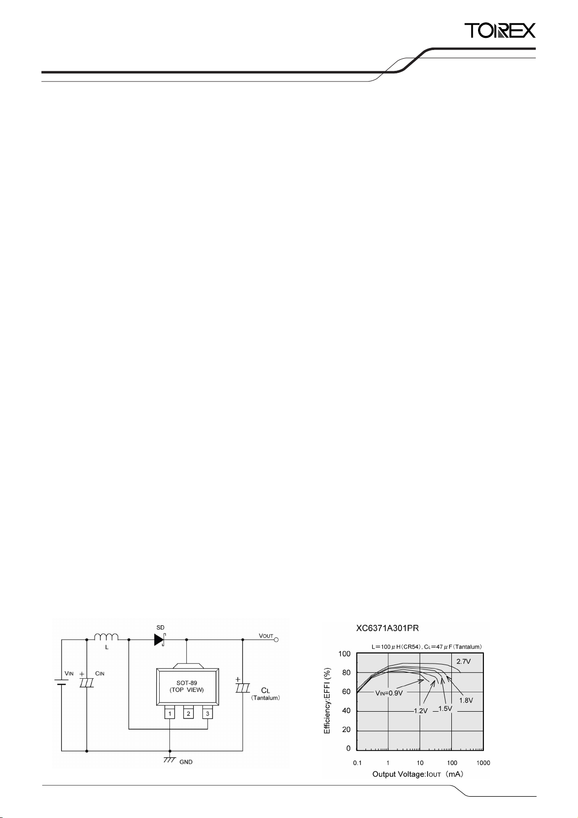
TYPICAL APPLICATION CIRCUIT
DD pin (separated power and voltage detect pins) are available.
■FEATURES
Operation Start Voltage Range
Output Voltage Range :
Highly Accurate : Setting voltage accuracy±2.5%
Oscillation Frequency :
selectable (XC6371/72)
30kHz (XC6373)
Maximum Output Currents (Tr. built-in)
:
Highly Efficient (Tr. built-in)
Built-in switching transistor type.
Five-lead packaged units offer either chip enable or
independent V
Phase compensation and soft start-up circuits built-in.
CMOS Low Power Consumption
Small Packages : SOT-89, SOT-89-5,USP-6B
*: Performance depends on external components and
PCB layout.
OUT pin option.
: 0.9V~10V
50kHz, 100kHz, 180kHz (±15%)
100mA(TYP.) @ VIN=3.0V, V
:
85%(TYP.) @ VIN=3.0V, V
■TYPICAL PERFORMANCE
☆GO-Compatible
2.0V~7.0V in 100mV increments
OUT
=5.0V *
OUT
=5.0V *
1/19
XC6371/XC6372/XC6373
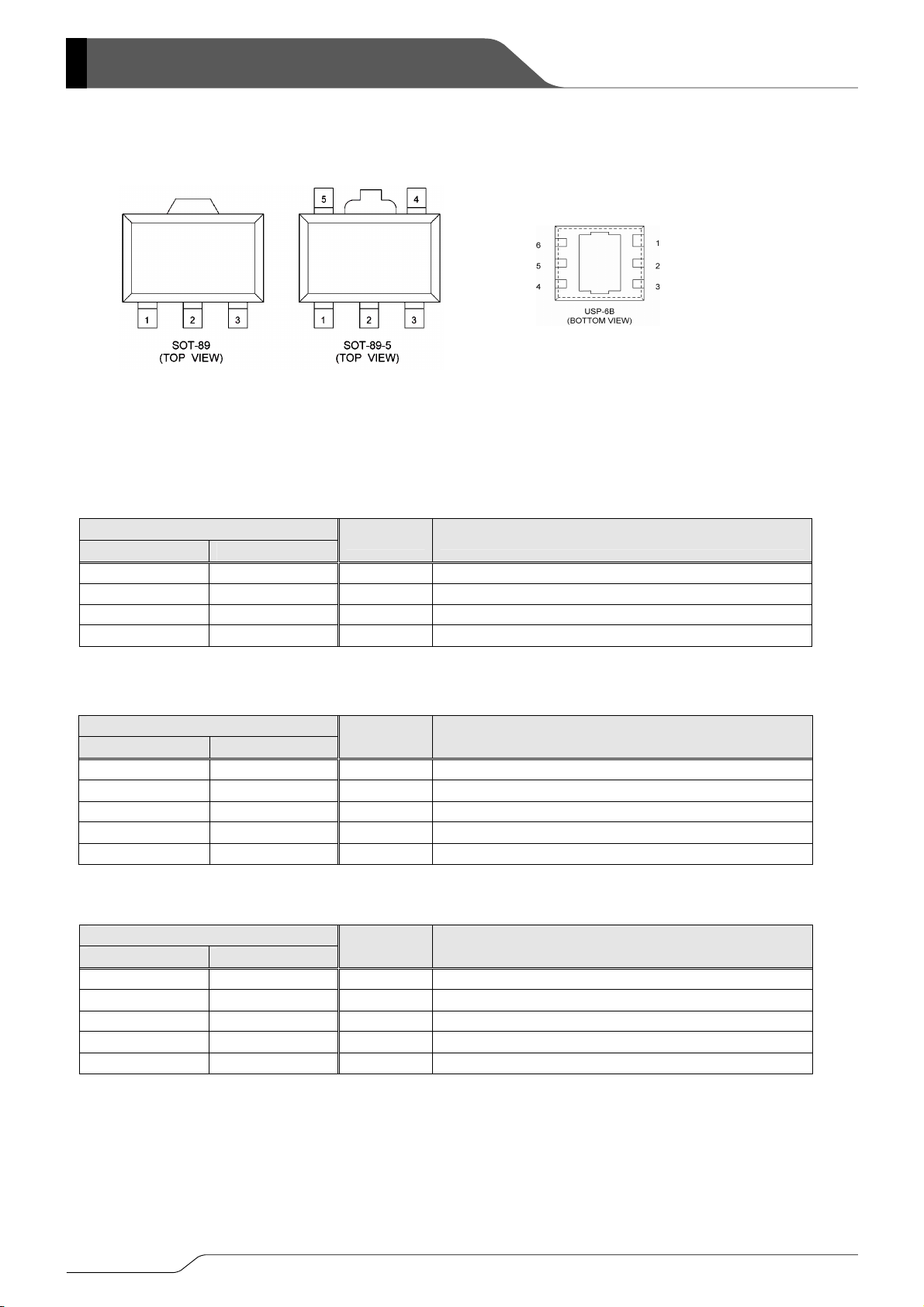
■PIN CONFIGURATION
Series
■PIN ASSIGNMENT
XC6371/72/73A
PIN NUMBER
SOT-89 USP-6B
PIN NAME FUNCTION
*The dissipation pad for the USP-6B
package should be solder-plated in
recommended mount pattern and metal
masking so as to enhance mounting
strength and heat release. If the pad needs
to be connected to other pins, it should be
connected to the pin No.1.
1 6 VSS Ground
2 1 VOUT
Output Voltage Monitor/IC Internal Power Supply
3 4 Lx Switch
-
XC6371/72/73C
SOT-89-5 USP-6B
PIN NUMBER
2, 3, 5 NC No Connection
PIN NAME FUNCTION
5 6 VSS Ground
2 1 VOUT Output Voltage Monitor/IC Internal Power Supply
4 4 Lx Switch
3 3 CE Chip Enable
1 2, 5 NC No Connection
XC6371/72/73E
PIN NUMBER
SOT-89-5 USP-6B
PIN NAME FUNCTION
5 6 VSS Ground
2 1 VDD IC Internal Power Supply
4 4 Lx Switch
3 3 VOUT Output Voltage Monitor
1 2, 5 NC No Connection
2/19
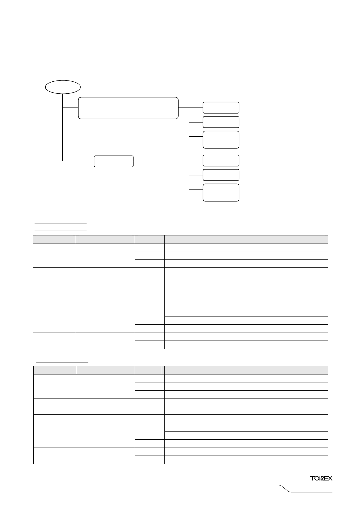
■PRODUCT CLASSIFICATION
●Selection Guide
START
PWM
XC6371
Low Frequency PWM XC6373
PWM/PFM
Standard
Chip Enable
Separated
V
DD/VOUT
Standard
Chip Enable
Separated
V
DD/VOUT
●Ordering Information
XC6371①②③④⑤⑥ : PWM controlled
XC6372①②③④⑤⑥
XC6371 Series
DESIGNATOR DESCRIPTION SYMBOL DESCRIPTION
①
: PWM/PFM switching control
Type of
DC/DC Converter
A : 3-pin DC/DC converter with built-in switching transistor
C : Stand-by capability with built-in switching transistor
E : Separated VDD and VOUT with built-in switching transistor
XC6371/XC6372/XC6373
Series
XC6371/73A
XC6371/73C
XC6371/73E
XC6372A
XC6372C
XC6372E
② ③
④
⑤
⑥
Output Voltage Integer
Oscillation Frequency
Package
Device Orientation
XC6373①②③④⑤⑥ : PWM controlled
DESIGNATOR
①
②
③
④
⑤
⑥
DESCRIPTION
Type of
DC/DC Converter
Output Voltage Integer
Oscillation Frequency 0
Package
Device Orientation
OUT=3.5V→②=3, ③=5
: e.g. V
0 : 50kHz
1 : 100kHz
2 : 180kHz
P
: SOT-89 (XC6371/72 A type)
: SOT-89-5 (XC6371/72 C/D type)
D : USP-6B
R : Embossed tape, standard feed
L : Embossed tape, reverse feed
SYMBOL
A
: 3-pin DC/DC converter with built-in switching transistor
DESCRIPTION
C : Stand-by capability with built-in switching transistor
E : Separated V
: e.g. V
DD and VOUT with built-in switching transistor
OUT=3.5V→②=3, ③=5
: 30kHz
P
D
R
L
: SOT-89 (XC6373 A type)
: SOT-89-5 (XC6373 C/D type)
: USP-6B
: Embossed tape, standard feed
: Embossed tape, reverse feed
3/19

(p)
XC6371/XC6372/XC6373
■BLOCK DIAGRAMS
XC6371/72/73A, C
■ABSOLUTE MAXIMUM RATINGS
OUT pin serves also as VDD)
(The V
Lx
VLx limi ter
Buffer
V
SS
EXT
Note: The CE pin is only used with the XC6371C.
PWM Control
OSC 50/100/180KHz
Chip Enable
CE
XC6371/72/73E
Lx
VLx limi ter
Buffer
V
SS
EXT
Note: Built-in transistor type units use the Lx pin.
PWM Control
OSC 50/100/180KHz
PAR AMETER SYMBOL RATINGS UNITS
VOUT Input Voltage VOUT 12 V
LX pin Voltage VLX 12 V
LX pin Current ILX 400 mA
CE Input Voltage VCE 12 V
Power Dissipation
SOT-89, 89-5 500
USP-6B
VDD Input Voltage VDD 12 V
Operating Temperature Range Topr
Storage Temperature Range Tstg
Soft Start
Vref
Phase comp
+
-
Soft Start
Vref
Phase comp
+
-
Pd
Series
DD
V
V
DD
V
OUT
V
DD
V
OUT
Ta =2 5℃
100
mW
-30~+80 ℃
-40~+125 ℃
4/19
,
XC6371/XC6372/XC6373
Series
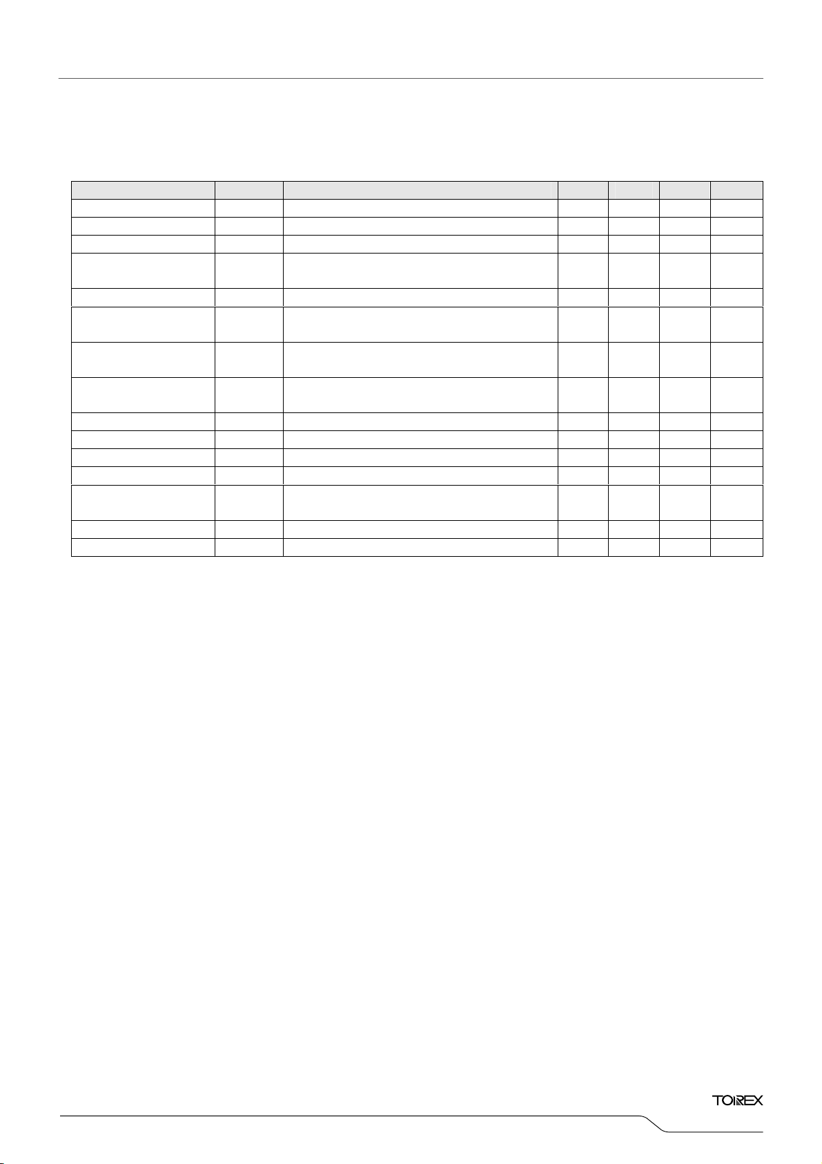
■ELECTRICAL CHARACTERISTICS
XC6371/72A501PR
PAR AMETER SYMBOL CONDITIONS MIN. TYP. MAX. UNITS
Output Voltage VOUT 4.875 5.000 5.125 V
Maximum Input Voltage VIN 10 - - V
Operation Start Voltage VST1 External Components Connected, IOUT=1mA - - 0.90 V
Oscillation Start Voltage VST2
No Load Input Current IIN
Supply Current 1 IDD1
Supply Current 2 IDD2
Lx Switch-On
Resistance
Lx Leak Current ILXL No external components. VOUT=VLX=10V - - 1.0
Oscillation Frequency FOSC Same as IDD1. Measuring of Lx waveform 85 100 115 kHz
Maximum Duty Ratio MAXDTY Same as IDD1. Measuring of Lx waveform 80 87 92 %
PFM Duty Ratio (*4) PFMDTY Same as IDD1. Measuring of Lx waveform 10 17 25 %
Lx Limit Voltage VLXLMT
Efficiency EFFI - 85 - %
Slow-Start Time TSS 4.0 10.0 20.0 mS
NOTE: Unless otherwise stated, VIN=VOUT×0.6, IOUT=50mA. See Typical Application Circuits, Circuit1
*1: The Schottky diode (SD) must be type MA735, with reverse current (IR)<1.0μA at reverse voltage (VR)=10.0V.(XC6372A)
*2: "Supply Current 1" is the supply current while the oscillator is continuously oscillating. In actual operation the oscillator periodically
operates which results in less average power consumption. The current actually provided by an external V
"No Load Input Current (I
*3: When PWM operates at PWM Mode.
*4: When PFM operates at PFM Mode.(XC6372A)
OUT=5.0V
V
RSWON Same as IDD1, VLX=0.4V - 1.4 2.4
FOSC=100kHZ
No external components. Apply voltage to VOUT
Lx : 10kΩ pull-up to 5V
IN=VOUT×0.8, IOUT=0mA (*1)
V
Same as VST2,
Apply output voltage×0.95 to VOUT
Same as VST2,
Apply output voltage×1.1 to V
OUT
Ta =2 5℃
- - 0.80 V
- 12.8 25.7
- 80.2 133.8
- 8.2 16.5
μA
μA
μA
Ω
μA
Same as IDD1. Apply output voltage to Lx,
Voltage required to produce FOSC×2
IN)".
0.7 - 1.3 V
IN source is represented by
5/19
)
XC6371/XC6372/XC6373
■ELECTRICAL CHARACTERISTICS (Continued
V
XC6371/72C501PR
OUT=5.0V, FOSC=100kHz Ta=25℃
Series
PAR AMETER SYMBOL CONDITIONS MIN. TYP. MAX. UNITS
Output Voltage VOUT 4.875 5.000 5.125 V
Maximum Input Voltage VIN 10 - - V
Operation Start Voltage VST1 External Components Connected, IOUT=1mA - - 0.90 V
Operation Start Voltage VST2
No Load Input Current IIN
Supply Current 1 IDD1
Supply Current 2 IDD2
Lx Switch-On
Resistance
R
SWON Same as IDD1, VLx=0.4V - 1.4 2.4
Lx Leak Current ILXL No external components, VOUT =VLX=10V - - 1.0
No external components. Apply voltage to VOUT,
Lx : 10kΩ pull-up to 5V
IN=VOUT×0.8, IOUT=0mA (*1)
V
Same as VST2,
Apply output voltage×0.95 to VOUT
Same as V
Apply output voltage×1.1 to V
ST2,
OUT
- - 0.80 V
- 12.8 25.7
- 80.2 133.8
- 8.2 16.5
μA
μA
μA
Ω
μA
Oscillation Frequency FOSC Same as IDD1, Measuring of Lx waveform 85 100 115 kHZ
Maximum Duty Ratio MAXDTY Same as IDD1, Measuring of Lx waveform 80 87 92 %
PFM Duty Ratio (*4) PFMDTY Same as IDD1, Measuring of Lx waveform 10 17 25 %
Stand-by Current ISTB Same as IDD1 - - 0.5
μA
CE "High" Voltage VCEH Same as IDD1, Lx Oscillation start 0.75 - - V
CE "Low" Voltage VCEL Same as IDD1, Lx Oscillation stop - - 0.20 V
CE "High" Current ICEH
Same as I
DD1, VCE=VOUT×0.95
CE "Low" Current ICEL Same as IDD1, VCE=0V - - -0.25
Lx Limit Voltage VLxLMT
Same as IDD1, Apply output voltage to Lx,
Voltage required to produce FOSC×2
- - 0.25
μA
μA
0.7 - 1.3 V
Efficiency EFFI - 85 - %
Slow-Start Time TSS 4.0 10.0 20.0 ms
NOTE: Unless otherwise stated, connect CE to VOUT, VIN=VOUT×0.6, IOUT=50mA. See Typical Application Circuits, Circuit 2.
*1: The Schottky diode (SD) must be type MA735, with reverse current (I
*2: "Supply Current 1" is the supply current while the oscillator is continuously oscillating. In actual operation the oscillator periodically
operates which results in less average power consumption. The current actually provided by an external VIN source is represented by
"No Load Input Current (I
*3: When PWM operates at PWM Mode.
*4: When PFM operates at PFM Mode.(XC6372C)
IN)".
R)<1.0μA at reverse voltage (VR)=10.0V.(XC6372C)
6/19

)
XC6371/XC6372/XC6373
Series
■ELECTRICAL CHARACTERISTICS (Continued
XC6371/72E501PR
PAR AMETER SYMBOL CONDITIONS MIN. TYP. MAX. UNITS
Output Voltage VOUT 4.875 5.000 5.125 V
Maximum Input Voltage VIN 10 - - V
Operation Start Voltage VST1 External Components Connected, IOUT=1mA - - 0.90 V
Oscillation Start Voltage VST2
No Load Input Voltage IIN
Supply Current 1 IDD1
Supply Current 2 IDD2
Lx Switch-On
Resistance
Lx Leak Current ILXL No external components, VOUT =VLX=10V - - 1.0
Oscillation Frequency FOSC Same as IDD1, Measuring of Lx waveform 85 100 115 kHZ
Maximum Duty Ratio MAXDTY Same as IDD1, Measuring of Lx waveform 80 87 92 %
PFM Duty Ratio (*4) PFMDTY Same as IDD1, Measuring of Lx waveform 10 17 25 %
Lx Limit Voltage VLxLMT
Efficiency EFFI - 85 - %
Slow-Start Time TSS 4.0 10.0 20.0 ms
NOTE: Unless otherwise stated, connect VDD to VOUT, VIN=VOUT×0.6, IOUT=50mA. See Typical Application Circuits, Circuit 3.
*1: The Schottky diode (SD) must be type MA2Q735, with reverse current (I
*2: "Supply current 1" is the supply current while the oscillator is continuously oscillating. In actual operation the oscillator periodically
operates which results in less average power consumption. The current actually provided by external V
Load Input Current (I
*3: When PWM operates at PWM Mode.
*4: When PFM operates at PFM Mode.(XC6372E)
*5: When the V
V
DD=0.8V. However, output voltage and oscillation frequency are properly stabilized when VDD=2.2V or higher.
DD and VOUT pins are independently used, the voltage range at the VDD pin should be 2.2V to 10V. The IC operates from
IN)".
VOUT=5.0V, FOSC=100kHz Ta=25℃
No external components,
Apply voltage to VOUT, Lx:10kΩpull-up to 5V
IN=VOUT×0.8, IOUT=0mA(*1)
V
Same as VST2,
Apply output voltage×0.95 to V
Same as V
ST2,
OUT
Apply output voltage×1.1 to VOUT
RSWON Same as IDD1, VLX=0.4V - 1.4 2.4
- - 0.80 V
- 12.8 25.7
- 80.2 133.8
- 8.2 16.5
μA
μA
μA
Ω
μA
Same as IDD1, Apply output voltage to Lx,
Voltage required to produce FOSC×2
R)<1.0μA at reverse voltage (VR)=10.0V.(XC6372E)
0.7 - 1.3 V
IN source is represented by "No
7/19

,
XC6371/XC6372/XC6373
■ELECTRICAL CHARACTERISTICS (Continued)
XC6373A300PR
VOUT=3.0V, FOSC=30kHz
Series
Ta =2 5℃
PAR AMETER SYMBOL CONDITIONS MIN. TYP. MAX. UNITS
Output Voltage VOUT 2.925 3.000 3.075 V
Maximum Input Voltage VIN 10 - - V
Operation Start Voltage VST1
Oscillation Start Voltage VST2
Supply Current 1 IDD1
Supply Current 2 IDD2
Lx Switch-On Resistance RSWON Same as IDD1, VLX=0.4V - 3.4 5.7
Lx Leak Current ILXL
External Components Connected,
I
OUT=1mA
No external components,
Apply voltage to VOUT, LX :10kΩpull-up to 5V
Same as VST2.
Apply output voltage×0.95 to V
OUT
Same as VST2,
Apply output voltage×1.1 to VOUT
No external components,
V
OUT =VLX=10V
- - 0.90 V
- - 0.80 V
- 13.1 21.9
- 3.9 7.9
μA
μA
Ω
- - 1.0
μA
Oscillation Frequency FOSC Same as IDD1, Measuring of Lx waveform 24 30 36 kHZ
Maximum Duty Ratio MAXDTY Same as IDD1, Measuring of Lx waveform 80 87 92 %
Efficiency EFFI - 77 - %
Slow-Start Time TSS 4.0 10.0 20.0 mS
NOTE: Unless otherwise stated, VIN=VOUT×0.6, IOUT=15mA. See Typical Application Circuits, Circuit 1.
V
XC6373A330PR
OUT=3.3V
FOSC=30kHz
Ta =2 5℃
PAR AMETER SYMBOL CONDITIONS MIN. TYP. MAX. UNITS
Output Voltage VOUT 3.128 3.300 3.383 V
Maximum Input Voltage VIN 10 - - V
Operation Start Voltage VST1 External Components Connected, IOUT=1mA - - 0.90 V
Oscillation Start Voltage VST2
Supply Current 1 IDD1
Supply Current 2 IDD2
Lx Switch-On
Resistance
RSWON Same as IDD1. VLX=0.4V - 3.4 5.7
Lx Leak Current ILXL
Oscillation Frequency FOSC
Maximum Duty Ratio MAXDTY
Apply voltage to VOUT, LX :10kΩpull-up to 5V
No external components,
Same as V
ST2,
Apply output voltage×0.95 to VOUT
Same as VST2,
Apply output voltage×1.1 to V
OUT
No external components,
V
OUT =VLX=10V
Same as IDD1,
Measuring of Lx waveform
Same as IDD1,
Measuring of Lx waveform
- - 0.80 V
- 14.1 23.5
- 4.0 8.1
μA
μA
Ω
- - 1.0
μA
24 30 36 kHZ
80 87 92 %
Efficiency EFFI - 77 - %
Slow-Start Time TSS 4.0 10.0 20.0 mS
NOTE: Unless otherwise stated, VIN=VOUT×0.6, IOUT=16.5mA. See Typical Application Circuits, Circuit 1.
8/19

(
)
(
)
■TYPICAL APPRICATION CIRCUITS
Circuit 1: XC6372A series
L : 100μH (CR54, SUMIDA) L : 100μH (CR54, SUMIDA)
L : 100μH (CR54, SUMIDA)
SD : MA2Q735 (Schottky Diode; MATUSHITA)
C
L : 16V47μF
Circuit 3: XC6372E series
Tantalum Capacitor, NICHICHEMI MCE
L : 100μH (CR54, SUMIDA)
SD : MA2Q735 (Schottky Diode; MATUSHITA)
C
L : 16V 47μF (Tantalum Capacitor; NICHICHEMI MCE)
XC6371/XC6372/XC6373
Circuit 2: XC6372C series
SD : MA2Q735 (Schottky Diode; MATUSHITA)
C
L : 16V 47μF
Tantalum Capacitor, NICHICHEMI MCE
Series
9/19

R
0
R
R
XC6371/XC6372/XC6373
Series
■TYPICAL PERFORMANCE CHARACTERISTICS
(1) Output Voltage vs. Output Current
(V)
OUT
5.2
5.1
5.0
XC6371A501P
L=100μH(CR54),CL=47μF(Tantalum)
1.5V1.2V
V
IN
=0.9V
2.0V
4.0V
3.0V
XC6371A301PR
3.10
3.05
3.00
V
L=100μH(CR54),C
IN
=1.0V
1.2V
4.9
Output Voltage:V
4.8
0.1 1 10 100 1000
Output Current:I
OUT
(mA)
2.95
Output Voltage:VOUT(V)
2.90
0.1 1 1 0 100 1000
Output Current:IOUT(mA)
5.2
(V)
5.1
OUT
5.0
4.9
Output Voltage:V
4.8
XC6372A501P
L=100μH(CR54),CL=47μF(Tantalum)
1.5V
V
IN
1.2V
=0.9V
0.1 1 10 100 1000
Output Current:I
OUT
2.0V
3.0V
4.0V
1000
(mA)
XC6372A301P
3.10
(V)
3.05
OUT
3.00
2.95
Output Voltage:V
2.90
L=100μH(CR54),CL=47μF(Tantalum)
VIN=0.9V
0.1 1 10 100 100
Output Current:I
XC6373A300PR
L=100μH(CR54),C
L=100μH(CR54), C
V
IN
=0.9V
)
(
V
OUT
3.10
3.05
3.00
2.95
Output Voltage: V
2.90
0.1 1 10 100 1000
Output Current: I
1.2V
L
=47μF(タンタル)
L
=
1.5V
47μF(Tantalum)
1.8V
2.7V
OUT
(mA)
L
=47μF(Tantalum)
1.5V
2.7V
1.5V
1.2V
OUT
(mA)
1.8V
1.8V
2.7V
10/19

0
R
0
R
0
R
XC6371/XC6372/XC6373
■TYPICAL PERFORMANCE CHARACTERISTICS (Continued)
(2) Efficiency vs. Output Current
XC6371A501P
100
80
60
40
20
Efficiency:EFFI(%)
L=100μH(CR54),CL=47μF(Tantalum)
IN
=0.9V
V
1.2V
0
0.1 1 10 100 100
Output Current:I
OUT
XC6373A300P
100
L=100μH(CR54), C
80
60
VIN=0.9V
40
20
Efficiency: EFFI (%)
0
0.1 1 10 100 100
Output Current: I
1.2V
L
=
47μF(Tantalum)
1.5V
OUT
1.5V
(mA)
2.7V
1.8V
(mA)
4.0V
3.0V
2.0V
1000
1000
XC6371A301P
100
80
60
40
20
Efficiency:EFFI(%)
L=100μH(CR54),CL=47μF(Tantalum)
2.7V
IN
=0.9V
V
1.2V
1.5V
1.8 V
0
0.1 1 10 100 100
Output Current:I
OUT
(mA)
1000
Series
11/19

0
R
0
R
r
XC6371/XC6372/XC6373
■TYPICAL PERFORMANCE CHARACTERISTICS (Continued)
(3) Ripple Voltage vs. Output Current
XC6373A300P
100
80
60
40
20
Ripple Voltage: Vr (mVp-p)
0
L=100μH(CR54), C
1.2V
VIN=0.9V
0.1 1 10 100 100
Output Current: I
L
1.5V
10
=
47μF(Tantalum)
1.8V
OUT
2.7V
1000
(mA)
Series
100
80
(mVp-p)
60
40
20
Ripple Voltage:V
XC6371A301P
L=100μH(CR54),CL=47μF(Tantalum)
1.8V
1.5V
1.2V
VIN=0.9V
0
0.1 1 10 100 100
Output Current:I
OUT
2.7V
(mA)
1000
12/19

XC6371/XC6372/XC6373
■TYPICAL PERFORMANCE CHARACTERISTICS (Continued)
(4) No Load Input Current vs. Input Voltage
XC6372A501PR
200
150
(μA)
IN
100
50
Input Current:I
L=100μH(CR54),CL=47μF(Tantalum)
0
012345
Input Voltage:VIN (V)
XC6371A301PR
500
400
(μA)
IN
300
200
100
Input Current:I
L=100μH(CR54),CL=47μF(Tantalum)
0
01
Input Voltage:VIN (V)
23
Series
13/19

XC6371/XC6372/XC6373
■TYPICAL PERFORMANCE CHARACTERISTICS (Continued)
(5) Operation Start Voltage / Hold Voltage vs. Output Current
(6) Load Transient Response
Series
14/19

■PACKAGING INFORMATION
●SOT-89
●USP-6B
XC6371/XC6372/XC6373
Series
●SOT-89-5
15/19

(
XC6371/XC6372/XC6373
■PACKAGING INFORMATION (Continued)
●USP-6B Recommended Pattern Layout
■MARKING RULE
[XC6371/72]
●SOT-89, SOT-89-5
②①
④③
① Represents product series
MARK PRODUCT SERIES MARK PRODUCT SERIES
Series
●USP-6B Recommended Metal Mask Design
A XC6371A 1 XC6372A
A XC6371C 1 XC6372C
S XC6371E 3 XC6372E
123
SOT-89
(TOP VIEW)
SOT-89-5
TOP VIEW)
② Represents integer of output voltage and oscillation frequency
OUTPUT VOLTAGE (V)
1.x B 1 1
2.x C 2 2
3.x F 3 3
4.x E 4 4
5.x F 5 5
6.x H 6 6
7.x K 7 7
③ Represents decimal number of output voltage and oscillation frequency
OUTPUT VOLTAGE (V)
x.0 0 0 A
x.1 1 1 B
x.2 2 2 C
x.3 3 3 D
x.4 4 4 E
x.5 5 5 F
x.6 6 6 H
x.7 7 7 K
x.8 8 8 L
x.9 9 9 M
④ Represents production lot number
0 to 9, A to Z repeated (G, I, J, O, Q, W excepted).
OSCILLATION FREQUENCY
50kHz 100kHz 180kHz
OSCILLATION FREQUENCY
50kHz 100kHz 180kHz
16/19

■MARKING RULE (Continued)
[XC6371/72] (Continued)
●USP-6B
① Represents product series
② Represents product classification
USP-6B
(TOP VIEW)
③④ Represents output voltage (ex.)
⑤ Represents oscillation frequency
⑥ Represents production lot number
0 to 9, A to Z repeated (G, I, J, O, Q, W excepted)
Note: No character inversion used.
XC6371/XC6372/XC6373
Series
MARK PRODUCT SERIES
5 XC6371xxxxDx
2 XC6372xxxxDx
MARK PRODUCT SERIES
A
C
E XC6371E
MARK
③ ④
3 3 3.3
5 0 5.0
MARK OSCILLATION FREQUENCY (kHz)
0 50
1 100
2 180
XC6371A
XC6371C
OUTPUT VOLTAGE (V)
17/19

(
XC6371/XC6372/XC6373
■MARKING RULE (Continued)
〔XC6373〕
●SOT-89,SOT-89-5
②①
④③
123
SOT-89
(TOP VIEW)
SOT-89-5
TOP VIEW)
① Represents product series
MARK FUNCTION PRODUCT SERIES
A - Built-in Transistor XC6372AxxxPx
A CE Built-in Transistor XC6372CxxxPx
S Separated VDD and VOUT Built-in Transistor XC6372ExxxPx
② Represents integer of output voltage and oscillation frequency
OUTPUT VOLTAGE (V)
③ Represents decimal number of output voltage and oscillation frequency
OUTPUT VOLTAGE (V)
④ Represents production lot number
0 to 9, A to Z repeated (G, I, J, O, Q, W excepted).
Series
OSCILLATION FREQUENCY (PRODUCT SERIES)
30kHz (XC6373xxx0Px)
1.x B
2.x C
3.x F
4.x E
5.x F
6.x H
7.x K
OSCILLATION FREQUENCY (PRODUCT SERIES)
30kHz (XC6373xxx0Px)
x.0 0
x.1 1
x.2 2
x.3 3
x.4 4
x.5 5
x.6 6
x.7 7
x.8 8
x.9 9
18/19

XC6371/XC6372/XC6373
Series
1. The products and product specifications contained herein are subject to change without
notice to improve performance characteristics. Consult us, or our representatives
before use, to confirm that the information in this catalog is up to date.
2. We assume no responsibility for any infringement of patents, patent rights, or other
rights arising from the use of any information and circuitry in this catalog.
3. Please ensure suitable shipping controls (including fail-safe designs and aging
protection) are in force for equipment employing products listed in this catalog.
4. The products in this catalog are not developed, designed, or approved for use with such
equipment whose failure of malfunction can be reasonably expected to directly
endanger the life of, or cause significant injury to, the user.
(e.g. Atomic energy; aerospace; transport; combustion and associated safety
equipment thereof.)
5. Please use the products listed in this catalog within the specified ranges.
Should you wish to use the products under conditions exceeding the specifications,
please consult us or our representatives.
6. We assume no responsibility for damage or loss due to abnormal use.
7. All rights reserved. No part of this catalog may be copied or reproduced without the
prior permission of Torex Semiconductor Ltd.
19/19
 Loading...