

A
XC62K Series
ETR0313_004
Negative Voltage Regulators
■GENERAL DESCRIPTIO N
The XC62K series are highly precise, low power consumpti on, negative voltage regulators, manufactured us ing CMOS and
laser trimming technologies. The series achieves high output currents with small input-output voltage differentials, and
consists of a high precision voltage reference, an error correction circuit, and an output driver with current limitation.
SOT-23 (150mW), SOT-89 (500mW), USP-6B (100mW) and TO-92 (300mW) packages are available.
■
PPLICATIONS
●Battery powered equipment
●Portable & cellular phones
●Various portable equipment
●Power supply for GaAs applications
■
TYPICAL APPLICATION CIRCUIT
■FEATURES
Dropout Voltage : 0.12V@50mA
Maximum Output Curr en t
Output Voltage Range
Highly Accurate : Setting output voltage ±2%
Low Power Consumption
Output Voltage Temperature Characteristics
:
Line Regulation : 0.1%/V (TYP.)
CMOS Low Power Consumption
Packages : SOT-23
Environmentally Friendly
: 0.38V@100mA
: 100mA (within MAX. power
dissipation, V
:
-2.1V ~ -6.0V (0.1V increments)
-5.0, -4.0, -3.0V, -2.5V standard
(All other voltages are semi-custom)
(±1% for semi-custom products)
: 3.0μA @ VOUT= -5.0V (TYP.)
±100ppm/℃ (TYP.)
SOT-89
TO-92
USP-6B
: EU RoHS Compliant, Pb Free
■ TYPICAL PERFORMANCE
CHARACTERISTICS
(V
OUT
=-5.0V)
OUT= -5.0V)
1/17
r
XC62K Series
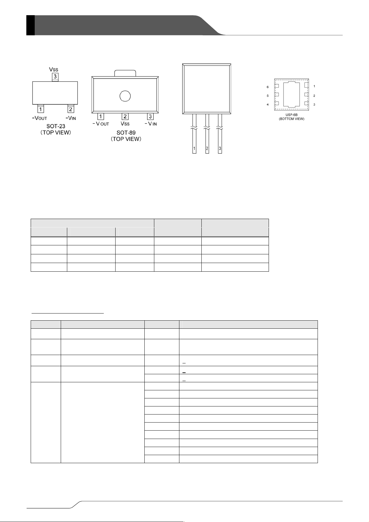
■PIN CONFIGURATION
■PIN ASSIGNMENT
PIN NUMBER
SOT-23 SOT-89/TO-92
2
3 6 -V
USP-6B
PIN NAME FUNCTION
-VOUT VSS -VIN
TO-92
(SIDE VIEW)
IN Power Supply Input
3 2 4 VSS Ground
1 1 2 -VOUT Output
- - 1.3.5 NC No Connection
■PRODUCT CLASSIFICATION
●Ordering Information
XC62K①②③④⑤⑥⑦-⑧
(*1)
MARK DESCRIPTION SYMBOL DESCRIPTION
①
②③
④
⑤
Polarity of Output Voltage N Negative
Output Voltage 21 ~ 60
Temperature Characteristics 0 +
Output Voltage Accuracy
1 + 1% (Semi-custom)
2 +
e.g. VOUT – 2.1V → ②=2, ③=1
100ppm (TYP.)
2%
V
OUT – 6.0V → ②=6, ③=0
MR SOT-23
MR-G SOT-23
PR SOT-89
PR-G SOT-89
⑥⑦-⑧
Packages
Taping Type
(*2)
TH TO-92:Paper type
TH-G TO-92:Paper type
TB TO-92:Bag type
TB-G TO-92:Bag type
DR USP-6B
DR-G USP-6B
(*1)
The “-G” suffix indicates that the products are Halogen and Antimony free as well as being fully RoHS compliant.
(*2)
The device orientation is fixed in its embossed tape pocket. For reverse orientation, please contact your local Torex sales office o
representative. (Standard orientation: ⑥R-⑧, Reverse orientation: ⑥L-⑧)
-VIN
NC
VSS
*The dissipation pad for the USP-6B
package should be solder-plated in
recommended mount pattern and metal
masking so as to enhance mounting
strength and heat release.
If the pad needs to be connected to other
pins, it should be connected to the V
NC
-VOUAT
NC
SS pin.
2/17
A
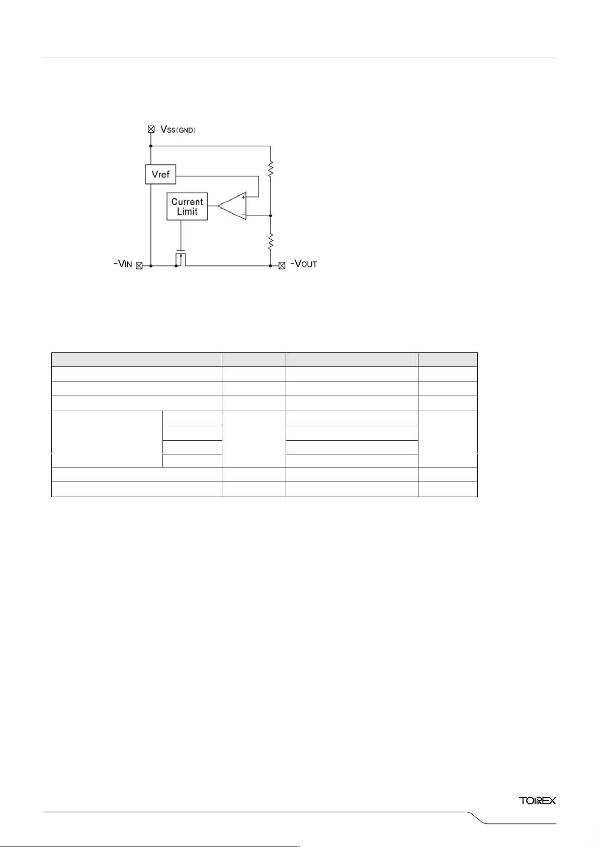
■BLOCK DIAGRAM
■
BSOLUTE MAXIMUM RATINGS
PARAMETER SYMBOL RATINGS UNITS
Input Voltage VIN -12.0 V
Output Current IOUT 200 mA
Output Voltage VOUT -VDD-0.3~VIN+0.3 V
Power Dissipation
USP-6B
Operating Temperature Range Topr -40 ~ +85
Storage Temperature Range Tstg -40 ~ +125
Ta=25℃
SOT-23 150
SOT-89 500
TO-92 300
Pd
mW
100
℃
℃
XC62K
Series
Note: Please ensure that IOUT is less than Pd/(VOUT-VIN).
3/17
XC62K Series
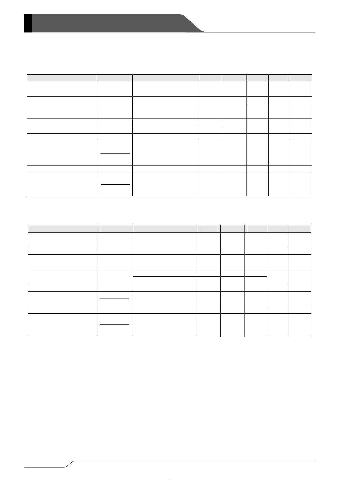
■ELECTRICAL CHARACTERISTICS
XC62KN5002
PARAMETER SYMBOL CONDITIONS MIN. TYP. MAX. UNITS
Output Voltage (*2) VOUT(E)
Maximum Output Current IOUT max
Load Regulation
Dropout Voltage (*3) Vdif
Supply Current ISS VIN=-6.0V - 3.0 7.0
OUT(T)=-5.0V
V
OUT
△V
IOUT=20mA
VIN=-6.0V
IN=-6.0V, VOUT(E)≧-4.5V
V
V
IN=6.0V
1mA≦IOUT≦50mA
IOUT=50mA - 120 300
I
OUT=100mA - 380 600
Ta=25℃
CIRCUIT
x 0.98
-4.90
VOUT(T)
-5.00
x 1.02
-5.10
V 2
100 - - mA 4
- 40 80 mV 4
mV 3
μA
1
Line Regulation
△V
Input Voltage VIN - - - -10.0 V -
Output Voltage
Temperature Characteristics
XC62KN4002
△V
OUT(T)=-4.0V
V
PARAMETER SYMBOL CONDITIONS MIN. TYP. MAX. UNITS
Output Voltage (*2) VOUT(E)
Maximum Output Current IOUT max
Load Regulation
Dropout Voltage (*3) Vdif
Supply Current ISS VIN=-5.0V - 3.0 6.5
Line Regulation
△V
Input Voltage VIN - - - -10.0 V -
△V
OUT
IN・VOUT
△V
OUT
IN・VOUT
OUT
△V
OUT
△V
IN・VOUT
IOUT=20mA
-6.0V≦VIN≦-10.0V
IOUT=20mA
-30℃≦Topr≦80℃
IOUT=20mA
V
IN=-5.0V
IN=-5.0V, VOUT(E)≧-3.6V
V
V
IN=-5.0V
1mA≦I
OUT≦45mA
- 0.1 0.3 %V 3
-
x 0.98
-3.92
±100
OUT(T)
V
-4.00
x 1.02
-4.08
80 - - mA 4
- 40 80 mV 4
IOUT=45mA - 120 300
I
OUT=90mA - 380 600
I
OUT=20mA
-5.0V≦V
IN≦-10.0V
- 0.1 0.3 %V 3
ppm/
℃
-
Ta=25℃
CIRCUIT
V 2
mV 3
μA
1
Output Voltage
Temperature Characteristics
NOTE:
*1: V
OUT(T)=Specified output voltage
*2: V
OUT(E)=Effective output voltage (i.e. the output voltage when "VOUT(T) -1.0V" is provided at the VIN pin while maintaining a certain IOUT
value).
*3: Vdif = {V
*4: V
*5: V
*6: I
IN1 - VOUT1}
OUT1 =A voltage equal to 98% of the output voltage whenever an amply stabilized IOUT {VOUT(T) -1.0V} is input.
IN1=The input voltage when a voltage equal to 98% of VOUT(E) appears. (Input voltage is gradually decreased.)
OUTMAX=Please ensure that output current is within the values given for power dissipation.
△V
△V
IN・VOUT
OUT
I
OUT=20mA
-30℃≦Topr≦80℃
-
±100
-
ppm/
℃
4/17
-
■ELECTRICAL CHARACTERISTICS (Continued)
XC62KN3002
V
OUT(T)=-3.0V
PARAMETER SYMBOL CONDITIONS MIN. TYP. MAX. UNITS
Output Voltage (*2) VOUT(E)
MAX. Output Current IOUT max
Load Regulation
△V
OUT
Dropout Voltage Vdif
IOUT=20mA
VIN=-4.0V
IN=-4.0V, VOUT(E)≧-2.7V
V
V
IN=-4.0V
1mA≦IOUT≦40mA
IOUT=40mA - 120 300
I
OUT=80mA - 380 600
x 0.98
Supply Current ISS VIN=4.0V - 2.5 6.0
Line Regulation
△V
△V
IN・VOUT
OUT
IOUT=20mA
-4.0V≦VIN≦-10.0V
Input Voltage VIN - - - -10.0 V -
XC62K
Series
Ta=25℃
CIRCUIT
VOUT(T)
-2.94
-3.00
60 - - mA 4
- 40 80 mV 4
- 0.1 0.3 %V 3
x 1.02
-3.06
V 2
mV 3
μA
1
Output Voltage
Temperature Characteristics
NOTE:
*1: V
OUT(T)=Specified output voltage
OUT(E)=Effective output voltage (i.e. the output voltage when "VOUT(T) -1.0V" is provided at the VIN pin while maintaining a certain IOUT
*2: V
value).
*3: Vdif = {V
*4: V
*5: V
*6: I
IN1 - VOUT1}
OUT1 =A voltage equal to 98% of the output voltage whenever an amply stabilized IOUT {VOUT(T) -1.0V} is input.
IN1=The input voltage when a voltage equal to 98% of VOUT(E) appears. (Input voltage is gradually decreased.)
OUTMAX=Please ensure that output current is within the values given for power dissipation.
△V
△V
IN・VOUT
OUT
IOUT=20mA
-30℃≦Topr≦80℃
-
±100
ppm/
-
℃
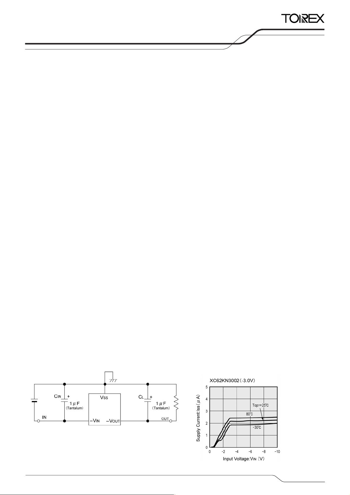
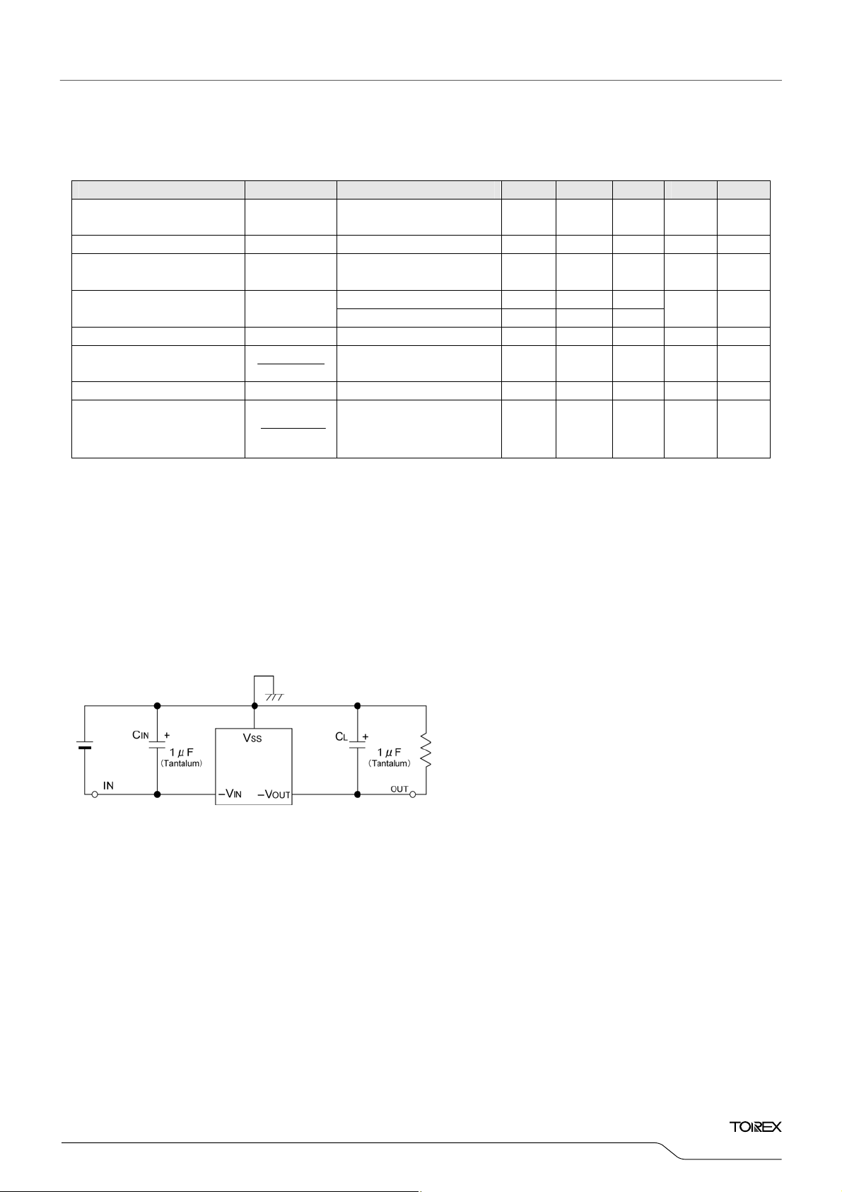
■TYPICAL APPLICATION CIRCUIT
-
■NOTES ON USE
Please ensure that values for input capacitance, CIN and out capacitance, CL, are more than 1μF (Tantalum).
5/17
XC62K Series
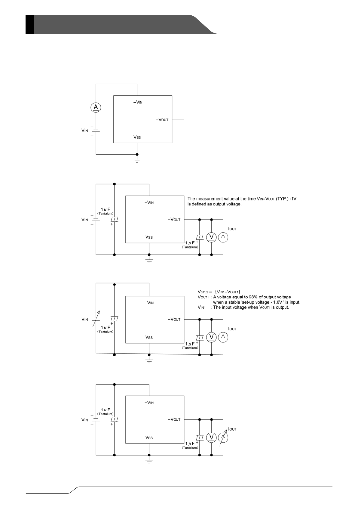
■TEST CIRCUITS
Circuit 1. Supply Current
Circuit 2. Output Voltage
Circuit 3. Line Regulation Dropout Voltage
Circuit 4. Load Regulation, Maximum Output Current
6/17

■TYPICAL PERFORMANCE CHARACTERISTICS
(1) Output Voltage vs. Output Current
XC62K
Series
XC62KN3002(-3.0V)
-
3.10
-
3.05
(V)
-
3.00
OUT
-
2.95
-
2.90
-
2.85
Output Voltage:V
-
2.80
0 20406080100
Output Current:I
OUT
VIN=-4.0V
Topr=-30℃
25℃
(mA)
80℃
7/17

XC62K Series
■TYPICAL PERFORMANCE CHARACTERISTICS (Continued)
(2) Output Voltage vs. Input Voltage
Output Voltage: VOUT(V)
XC62KN4002(-4.0V)
8/17

■TYPICAL PERFORMANCE CHARACTERISTICS (Continued)
(3) Dropout Voltage vs. Output Current
Dropout Voltage : Vdif (mV)
(4) Supply Current vs. Input Voltage
Dropout Voltage : Vdif (mV)
Dropout Voltage : Vdif (mV)
XC62K
Series
9/17

XC62K Series
■TYPICAL PERFORMANCE CHARACTERISTICS (Continued)
(5) Output Voltage vs. Ambient Temperature
(6) Supply Current vs. Ambient Temperature
(7) Input Transient Respon se 1
Ambient Temperature : Topr(℃) Ambient Temperature : Topr(℃) Ambient Temperature : To pr (℃)
Ambient Temperature : Topr(℃) Ambient Temperature : Topr(℃) Ambient Temperature : Topr(℃)
10/17

■TYPICAL PERFORMANCE CHARACTERISTICS (Continued)
(7) Input Transient Respon se 1
(8) Input Transient Respon se 2
XC62K
Series
11/17

XC62K Series
■TYPICAL PERFORMANCE CHARACTERISTICS (Continued)
(9) Load Transient Response
(10) Ripple Rejection Rate
12/17

●
■PACKAGING INFORMATION
SOT-23
●TO-92
Paper type Bag
Unit : mm
Unit : mm
●SOT-89
XC62K
Series
Unit : mm
13/17

XC62K Series
■PACKAGING INFORMATION (Continued)
●USP-6B
Unit : mm
●USP-6B Reference Pattern Layout
●USP-6B Reference Metal Mask Design
14/17

r
■ MARKING RULE
●SOT-23, SOT-89
3
① ② ③ ④
12
SOT-23
(TOP VIEW)
②①
●TO-92
123
SOT-89
(TOP VIEW)
TO-92
(SIDE VIEW)
④③
① represents integral number of output voltage
MARK VOLTAGE (V) MARK VOLTAGE (V)
2 2.X 5 5.X
3 3.X 6 6.X
4 4.X
② represents decimal number of output voltage
MARK VOLTAGE (V) MARK VOLTAGE (V)
A x.0 F x.5
B x.1 H x.6
C x.2 K x7
D x.3 L x.8
E x.4 M x.9
③ represents polarity of output voltage
MARK POLARITY
5 Negative
④ represents production lot number
0 to 9, A to Z repeated, reverse character 0 to 9, A to Z repeated
(G, I, J, O, Q, W excluded)
① represents polarity of output voltage
MARK OUTPUT CONFIGURATION
N
- (Negative)
②③ represents output voltage (ex.)
MARK
② ③
VOLTAGE (V)
3 3 3.3
5 0 5.0
④
epresents temperature characteristics
MARK
TEMPERATURE
CHARACTERISTICS
0 +100 ppm (TYP.)
⑤ represents output voltage accuracy
MARK OUTPUT VOLTAGE ACCURACY
1 Within +1% (semi-custom)
2 Within +2%
⑥ represents least significant digit of production year (ex.)
MARK PRODUCTION YEAR
3 2003
4 2004
⑦ represents production lot number
0 to 9, A to Z repeated (G, I, J, O, Q, W excluded)
XC62K
Series
15/17

XC62K Series
■ MARKING RULE (Continued)
●USP-6B
① represents production series
MARK PRODUCT SERIES
K XC62KNxx0xDx
② represents polarity of output voltage
MARK POLARITY PRODUCT SERIES
USP-6B
(TOP VIEW)
N
-(Negative)
XC62KNxx0xDx
③④ represents output voltage (ex.)
MARK
③ ④
VOLTAGE (V) PRODUCT SERIES
3 3 3.3 XC62KN330xDx
5 0 5.0 XC62KN500xDx
⑤ represents temperature characteristics
MARK
TEMPERATURE
CHARACTERISTICS
PRODUCT SERIES
0 + 100 ppm (TYP.) XC62KNxx0xDx
⑥ represents production lot number
0 to 9, A to Z repeated (G, I, J, O, Q, W excluded)
Note: No character inversion used.
16/17

XC62K
Series
1. The products and prod uct specifications cont ained herein are subject to change without
notice to improve performance characteristics. Consult us, or our representatives
before use, to confirm that the information in this datasheet is up to date.
2. We assume no responsibility for any infringement of patents, patent rights, or other
rights arising from the use of any information and circuitry in this datasheet.
3. Please ensure suitable shipping controls (including fail-safe designs and aging
protection) are in force for equipment employing products listed in this datasheet.
4. The products in this datasheet are not developed, designed, or approved for use with
such equipment whose failure of malfunction can be reasonably expected to directly
endanger the life of, or cause significant injury to, the user.
(e.g. Atomic energy; aerospace; transport; combustion and associated safety
equipment thereof.)
5. Please use the products listed in this datasheet within the specified ranges.
Should you wish to use the products under conditions exceeding the specifications,
please consult us or our representatives.
6. We assume no responsibility for damage or loss due to abnormal use.
7. All rights reserved. No part of this datasheet may be copied or reproduced without the
prior permission of TOREX SEMICONDUCTOR LTD.
17/17
 Loading...