


TK71531SCL
TOKO TK71531SCL, TK71530SCL, TK71529SCL, TK71528SCL, TK71522SCL Datasheet
...
TK715xx
20P
LOW DROPOUT VOLTAGE REGULATOR
FEATURES
■ High Voltage Precision at ± 2.0% or ± 60 mV
■ Very Low Quiescent Current
■ Very Low Dropout Voltage
■ Reverse Bias Protection
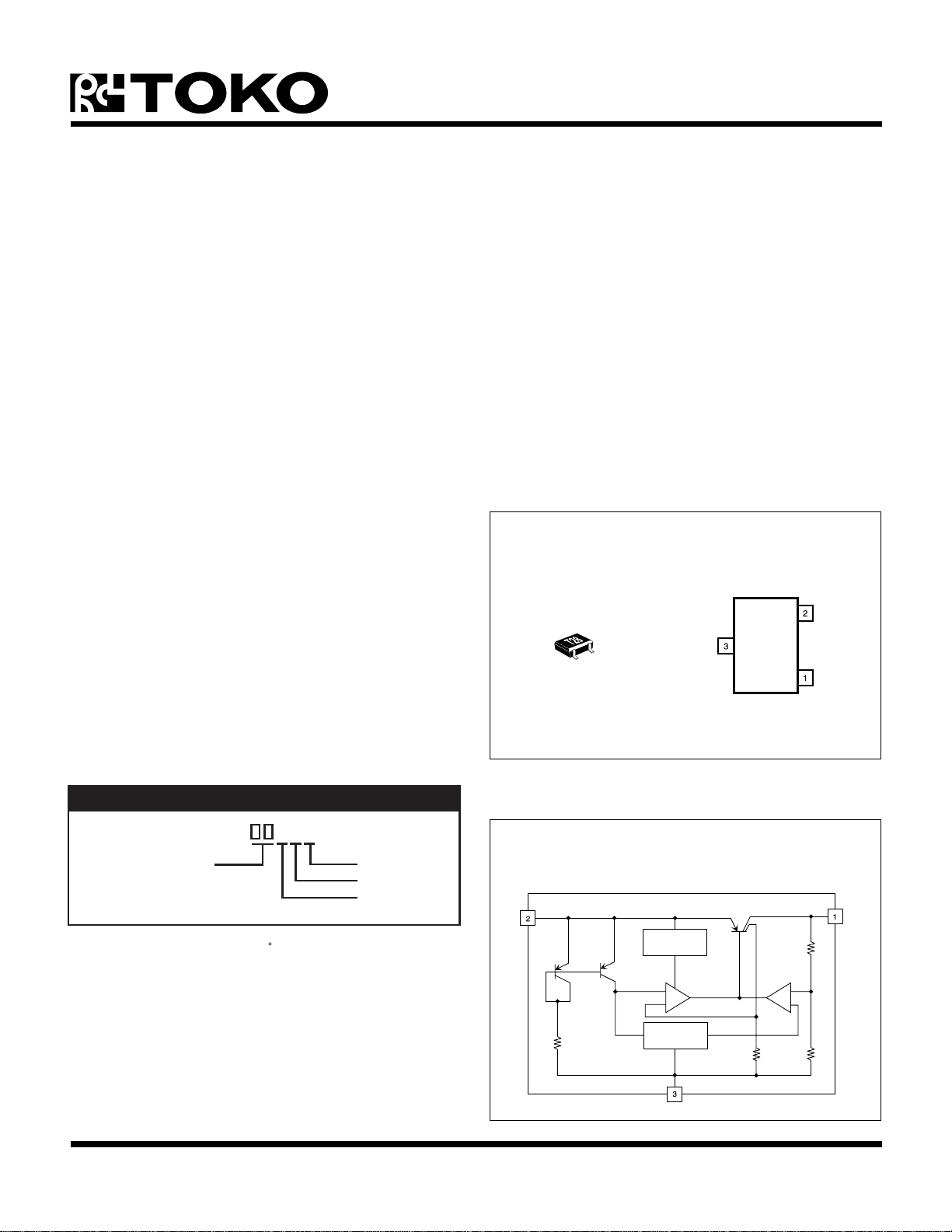
■ Miniature Package (SOT-23-3)
■ Short Circuit Protection
■ High Ripple Rejection
DESCRIPTION
The TK715xx is a low dropout linear regulator housed in a
small SOT-23-3 package, rated at 350 mW. An internal
PNP transistor is used to achieve a low dropout voltage of
105 mV (typ.) at 50 mA load current. This device offers high
precision output voltage of ± 2.0 % or ± 60 mV. The
TK715xx has a very low quiescent current of 25 µA (typ.)
at no load. The low quiescent current and dropout voltage
make this part ideal for battery powered applications. The
internal reverse bias protection eliminates the requirement
for a reverse voltage protection diode, saving cost and
board space. The high 64 dB ripple rejection and low noise
provide enhanced performance for critical applications.
APPLICATIONS
■ Battery Powered Systems
■ Cellular Telephones
■ Pagers
■ Personal Communications Equipment
■ Portable Instrumentation
■ Portable Consumer Equipment
■ Radio Control Systems
■ Toys
■ Low Voltage Systems
TK715xxS
GND
V
V
IN
OUT
ORDERING INFORMATION
TK715 SCL
Voltage Code
VOLTAGE CODE
19 = 1.9 V 37 = 3.7 V
20 = 2.0 V 38 = 3.8 V
21 = 2.1 V 39 = 3.9 V
22 = 2.2 V 40 = 4.0 V
23 = 2.3 V 41 = 4.1 V
24 = 2.4 V 42 = 4.2 V
25 = 2.5 V 43 = 4.3 V
26 = 2.6 V 44 = 4.4 V
27 = 2.7 V 45 = 4.5 V
28 = 2.8 V 46 = 4.6 V
29 = 2.9 V 47 = 4.7 V
30 = 3.0 V 48 = 4.8 V
31 = 3.1 V 49 = 4.9 V
32 = 3.2 V 50 = 5.0 V
33 = 3.3 V 60 = 6.0 V
34 = 3.4 V 70 = 7.0 V
35 = 3.5 V 80 = 8.0 V
36 = 3.6 V 90 = 9.0 V
TEMPERATURE CODE
C -30 to +80 C
PACKAGE CODE
S : SOT-23-3
January 1999 TOKO, Inc. Page 1
Tape/ Reel Code
Temp. Code
Package Code
TAPE/REEL CODE
L: Tape Left
V
IN
BLOCK DIAGRAM
THERMAL
PROTECTION
+
BANDGAP
REFERENCE
GND
V
OUT
+
TK715xx
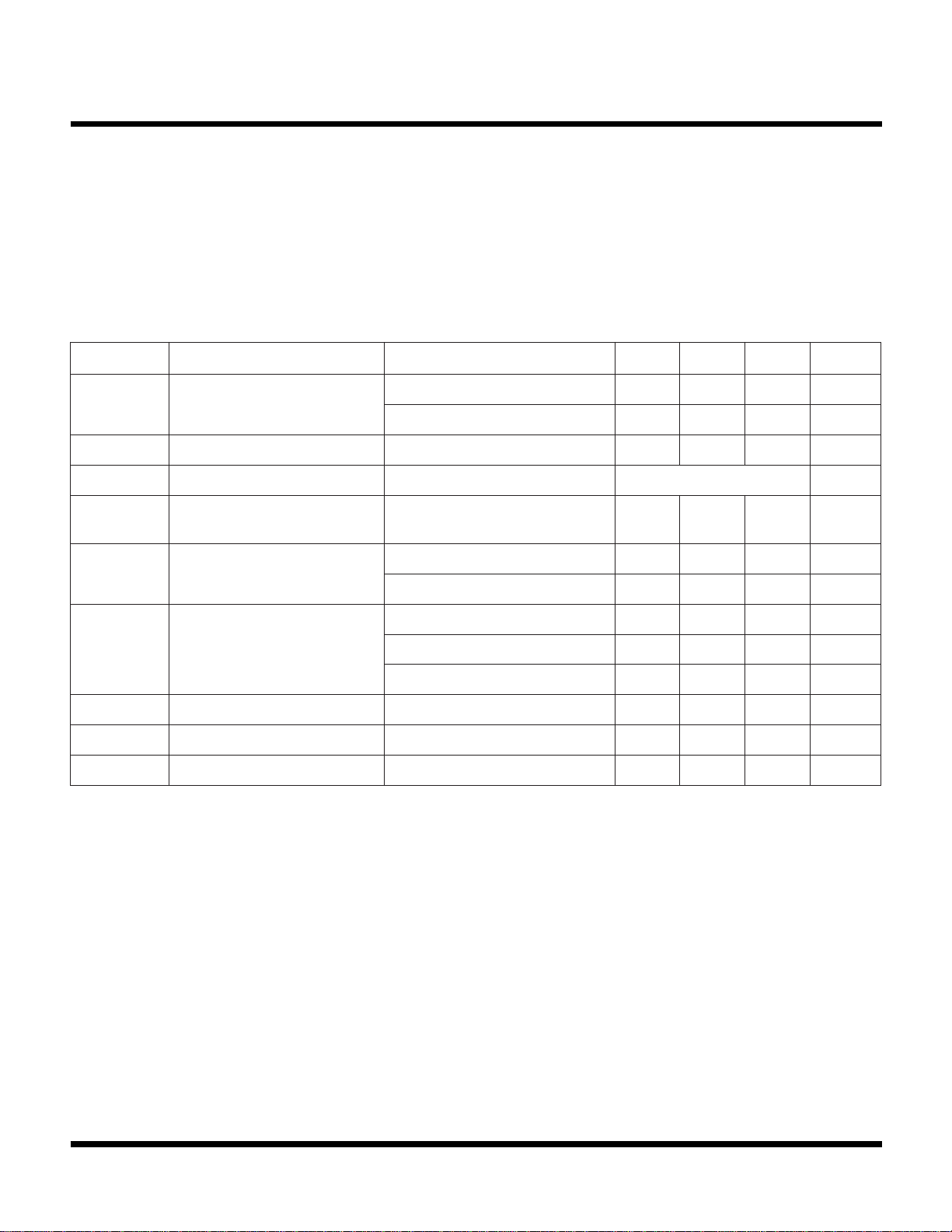
ABSOLUTE MAXIMUM RATINGS (V
Supply Voltage .............................................. -0.4 to 16 V
Power Dissipation (Note 1) ................................ 350 mW
Reverse Bias.............................................................. 8 V
Storage Temperature (Ambient) ...............-55 to +150 °C
OUT
≥ 5.0 V)
Max. Operating Temperature (Junction) ...............125 °C
Operating Voltage Range............................ 1.8 to 14.0 V
Junction Temperature ...........................................150 °C
Lead Soldering Temperature (10 s) ......................235 °C
Operating Temperature (Ambient) ..............-30 to +80 °C
TK715xx ELECTRICAL CHARACTERISTICS (V
Test conditions: T
= 25 °C, unless otherwise specified.
A
OUT
≥ 5.0 V)
LOBMYSRETEMARAPSNOITIDNOCTSETNIMPYTXAMSTINU
I
I
Q
I
DNG
V
TUO
tnerruCtnecseiuQ
tnerruCdnuorGI
egatloVtuptuOI
geReniLnoitalugeReniL
geRdaoLnoitalugeRdaoL
V
PORD
I
TUO
egatloVtuoporD
tnerruCtuptuOsuounitnoC 001Am
TUO
I
TUO
TUO
TUO
V
V=
NI
V
I
TUO
I
TUO
I
TUO
I
TUO
I
TUO
V,Am0=
≤ V0.45254Aµ
TUO
V,Am0=
≥ V1.40305Aµ
TUO
Am05=4.15.2Am
Am01=1elbaTeeSV
)PYT(TUO
V6+
)PYT(TUO
otV1+
0.101Vm
)2etoN(,Am05ot5=0103Vm
)2etoN(,Am001ot5=0205Vm
Am05=501.00810.V
V,Am001=
≥ V4.2581.0082.0V
TUO
V,Am001=
TUO
V4.2<581.0033.0V
RRnoitcejeRelppiR)4,3setoN(46Bd
∆V
/ ∆T
TUO
Note 1: Power dissipation is 350 mW when mounted as recommended. Derate at 2.8 mW/°C for operation above 25 °C.
Note 2: Refer to “Definition of Terms.”
Note 3: Ripple rejection and noise voltage are affected by the value and characteristics of the capacitor used.
Note 4: Ripple rejection is measured at VR = 200 mVrms, VIN = V
Gen. Note: Parameters with min. or max. values are 100% tested at TA = 25 °C.
tneiciffeoCerutarepmeTI
TUO
Am01=53C°/mpp
OUT(TYP)
+ 2 V, I
= 10 mA, CL = 4.7 µF, f = 100 Hz.
OUT
Page 2 January 1999 TOKO, Inc.
TK715xx
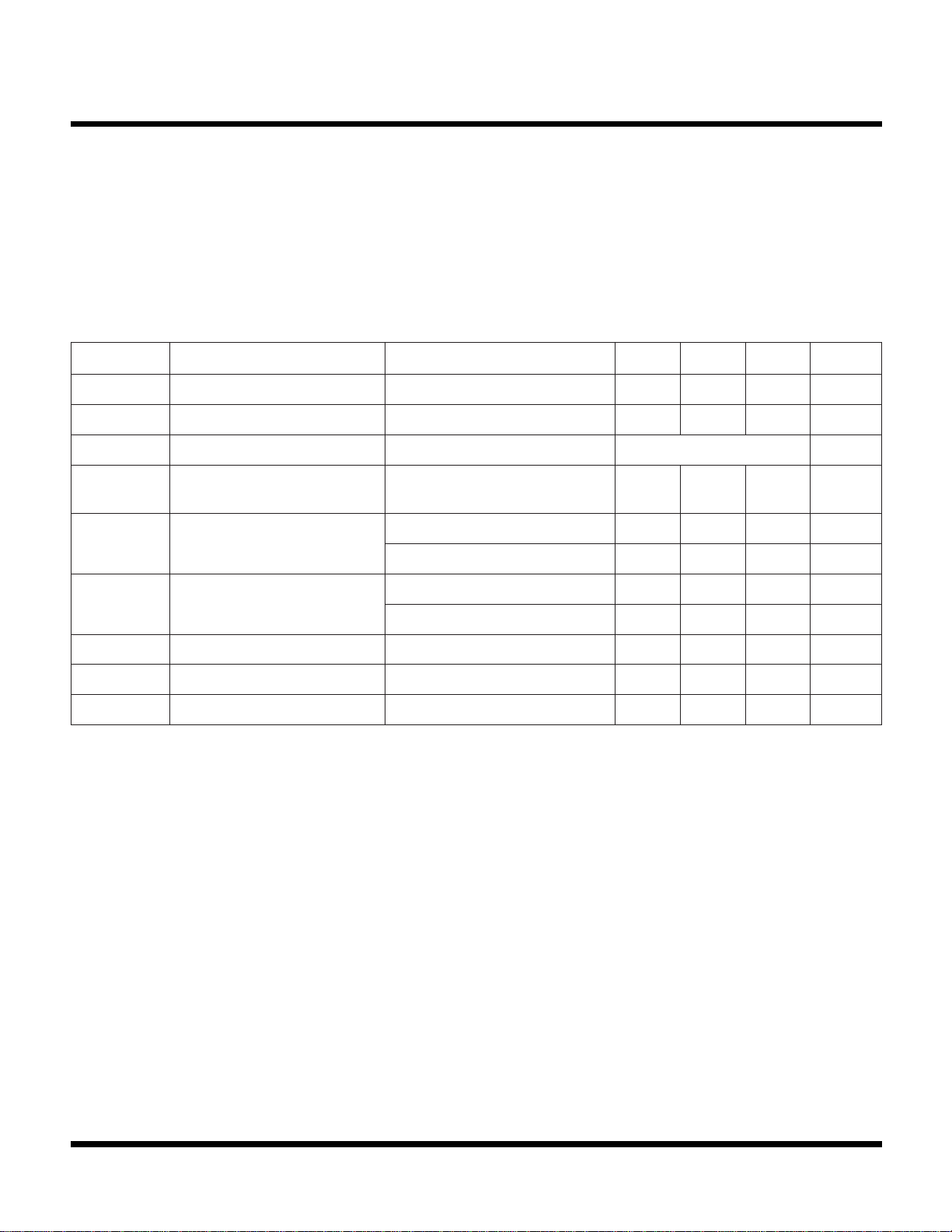
ABSOLUTE MAXIMUM RATINGS (V
Supply Voltage .............................................. -0.4 to 16 V
Power Dissipation (Note 1) ................................ 350 mW
Reverse Bias.............................................................. 8 V
Storage Temperature (Ambient) ...............-55 to +150 °C
OUT
≤ 6.0 V)
Max. Operating Temperature (Junction) ............... 125 °C
Operating Voltage Range............................ 2.5 to 14.0 V
Junction Temperature ...........................................150 °C
Lead Soldering Temperature (10 s) ......................235 °C
Operating Temperature (Ambient) ..............-30 to +80 °C
TK715xx ELECTRICAL CHARACTERISTICS (V
Test conditions: T
= 25 °C, unless otherwise specified.
A
OUT
≤ 6.0 V)
LOBMYSRETEMARAPSNOITIDNOCTSETNIMPYTXAMSTINU
I
Q
I
DNG
V
TUO
geReniLnoitalugeReniL
geRdaoLnoitalugeRdaoL
V
PORD
I
TUO
tnerruCtnecseiuQI
tnerruCdnuorGI
egatloVtuptuOI
TUO
TUO
TUO
V
NI
V
I
TUO
I
TUO
I
egatloVtuoporD
TUO
I
TUO
Am0=2306Aµ
Am05=4.15.2Am
Am01=1elbaTeeSV
V=
)PYT(TUO
)PYT(TUO
otV1+
V41xaMroV6+
)2etoN(,Am05ot5=0103Vm
)2etoN(,Am001ot5=0205Vm
Am05=501.00810.V
Am001=581.0082.0V
tnerruCtuptuOsuounitnoC 001Am
0.3Vm
RRnoitcejeRelppiR)4,3setoN(46Bd
/ ∆T
∆V
TUO
Note 1: Power dissipation is 350 mW when mounted as recommended. Derate at 2.8 mW/°C for operation above 25 °C.
Note 2: Refer to “Definition of Terms.”
Note 3: Ripple rejection and noise voltage are affected by the value and characteristics of the capacitor used.
Note 4: Ripple rejection is measured at VR = 200 mVrms, VIN = V
Gen. Note: Parameters with min. or max. values are 100% tested at TA = 25 °C.
tneiciffeoCerutarepmeTI
TUO
Am01=53C°/mpp
OUT(TYP)
+ 2 V, I
= 10 mA, CL = 4.7 µF, f = 100 Hz.
OUT
January 1999 TOKO, Inc. Page 3
TK715xx
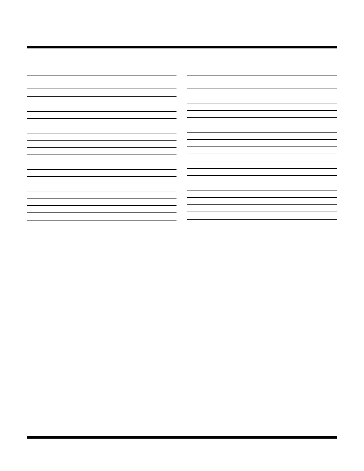
TK715xx ELECTRICAL CHARACTERISTICS TABLE 1
Output Voltage V
Voltage Code Voltage
OUT(MIN)
V
OUT(MAX)
Test
1.9 V 19 1.840 V 1.960 V 2.9 V
2.0 V 20 1.940 V 2.060 V 3.0 V
2.1 V 21 2.040 V 2.160 V 3.1 V
2.2 V 22 2.140 V 2.260 V 3.2 V
2.3 V 23 2.240 V 2.360 V 3.3 V
2.4 V 24 2.340 V 2.460 V 3.4 V
2.5 V 25 2.440 V 2.560 V 3.5 V
2.6 V 26 2.540 V 2.660 V 3.6 V
2.7 V 27 2.640 V 2.760 V 3.7 V
2.8 V 28 2.740 V 2.860 V 3.8 V
2.9 V 29 2.840 V 2.960 V 3.9 V
3.0 V 30 2.940 V 3.060 V 4.0 V
3.1 V 31 3.040 V 3.160 V 4.1 V
3.2 V 32 3.140 V 3.260 V 4.2 V
3.3 V 33 3.240 V 3.360 V 4.3 V
3.4 V 34 3.335 V 3.465 V 4.4 V
3.5 V 35 3.435 V 3.565 V 4.5 V
3.6 V 36 3.535 V 3.665 V 4.6 V
Output Voltage V
Voltage Code Voltage
OUT(MIN)
V
OUT(MAX)
Test
3.7 V 37 3.630 V 3.770 V 4.7 V
3.8 V 38 3.725 V 3.875 V 4.8 V
3.9 V 39 3.825 V 3.975 V 4.9 V
4.0 V 40 3.920 V 4.080 V 5.0 V
4.1 V 41 4.020 V 4.180 V 5.1 V
4.2 V 42 4.120 V 4.280 V 5.2 V
4.3 V 43 4.215 V 4.385 V 5.3 V
4.4 V 44 4.315 V 4.485 V 5.4 V
4.5 V 45 4.410 V 4.590 V 5.5 V
4.6 V 46 4.510 V 4.690 V 5.6 V
4.7 V 47 4.605 V 4.795 V 5.7 V
4.8 V 48 4.705 V 4.895 V 5.8 V
4.9 V 49 4.800 V 5.000 V 5.9 V
5.0 V 50 4.900 V 5.100 V 6.0 V
6.0 V 60 5.880 V 6.120 V 7.0 V
7.0 V 70 6.860 V 7.140 V 8.0 V
8.0 V 80 7.840 V 8.160 V 9.0 V
9.0 V 90 8.820 V 9.180 V 9.0 V
Page 4 January 1999 TOKO, Inc.
 Loading...