


TOKO TK11250BUIB, TK11250BUCB, TK11250BMIL, TK11250BMCL, TK11249BUIB Datasheet
...TK112xxB
VOLTAGE REGULATOR WITH ON/OFF SWITCH
FEATURES
■High Voltage Precision at ± 2.0%
■Active High On/Off Control
■Very Low Dropout Voltage 80 mV at 30 mA
■Very Low Noise
■Very Small SOT-23L or SOT-89 Surface Mount Packages
■Internal Thermal Shutdown
■Short Circuit Protection
APPLICATIONS
■Battery Powered Systems
■Cellular Telephones
■Pagers
■Personal Communications Equipment
■Portable Instrumentation
■Portable Consumer Equipment
■Radio Control Systems
■Toys
■Low Voltage Systems
DESCRIPTION
The TK112xxB is a low dropout linear regulator with a builtin electronic switch. The internal switch can be controlled by TTL or CMOS logic levels. The device is in the “on” state when the control pin is pulled to a logic high level. An external capacitor can be connected to the noise bypass pin to lower the output noise level to 30 Vrms.
An internal PNP pass transistor is used to achieve a low dropout voltage of 80 mV (typ.) at 30 mA load current. The TK112xxB has a very low quiescent current of 170 A at no load and 1 mA with a 30 mA load. The standby current is typically 100 nA. The internal thermal shut down circuitry limits the junction temperature to below 150 ° C. The load current is internally monitored and the device will shut down in the presence of a short circuit or overcurrent condition at the output.
ORDERING INFORMATION
TK112 |
B |
|
|
|
|
|
|
|
|
|
|
|
|
|
|
Tape/Reel Code |
|
|
|
|
|
|
|
|
|
|
|
|
|
|
|
||
Voltage Code |
|||||||||||||||
|
|
|
|
|
|
|
|
|
|
|
|
||||
Package Code |
|
|
|
|
|
|
|
|
|
|
|
|
Temp. Code |
||
|
|
|
|
|
|
|
|
|
|
|
|||||
VOLTAGE CODE
13 = 1.3 V |
33 = 3.3 V |
14 = 1.4 V |
34 = 3.4 V |
15 = 1.5 V |
35 = 3.5 V |
16 = 1.6 V |
36 = 3.6 V |
17 = 1.7 V |
37 = 3.7 V |
18 = 1.8 V |
38 = 3.8 V |
19 = 1.9 V |
39 = 3.9 V |
20 = 2.0 V |
40 = 4.0 V |
21 = 2.1 V |
41 = 4.1 V |
22 = 2.2 V |
42 = 4.2 V |
23 = 2.3 V |
43 = 4.3 V |
24 = 2.4 V |
44 = 4.4 V |
25 = 2.5 V |
45 = 4.5 V |
26 = 2.6 V |
46 = 4.6 V |
27 = 2.7 V |
47 = 4.7 V |
28 = 2.8 V |
48 = 4.8 V |
29 = 2.9 V |
49 = 4.9 V |
30 = 3.0 V |
50 = 5.0 V |
31 = 3.1 V |
55 = 5.5 V |
32 = 3.2 V |
80 = 8.0 V |
PACKAGE CODE:
M: SOT-23L
U: SOT-89
NOTE 1:
1.3 V to 1.9 V available
in SOT-23L package only.
NOTE 2:
1.3 V to 2.4 V available in C temperature code (-30 to +80 C) only.
TAPE/REEL CODE
L: Tape Left (SOT-23L)
B: Tape Left (SOT-89)
TEMP. CODE:
C: -30 to +80 C
I: -40 to +85 C
The TK112xxB is available in either a 6-pin SOT-23L or a 5-pin SOT-89 surface mount package.
20P
SOT-23L
TK112xxB
CONTROL |
|
|
|
|
|
VIN |
|
|
|
|
|
||
GND |
|
|
|
|
|
GND |
|
|
|
|
|
||
NOISE BYPASS |
|
|
|
|
|
VOUT |
|
|
|
|
|
||
|
|
|
|
|
|
|
|
NOISE BYPASS |
VOUT |
|
GND |
GND |
SOT-89 |
CONTROL |
VIN |
|
BLOCK DIAGRAM |
|
VIN |
|
VOUT |
|
THERMAL |
|
|
PROTECTION |
|
CONTROL |
|
|
|
BANDGAP |
|
|
REFERENCE |
|
|
|
GND |
|
NOISE |
|
|
BYPASS |
|
October 1999 TOKO, Inc. |
Page 1 |

TK112xxB
ABSOLUTE MAXIMUM RATINGS TK112xxBC (VOUT ≥ 2.0 V) |
|
° C |
||
Supply Voltage ......................................................... |
16 V |
Storage Temperature Range ................... |
-55 to +150 |
|
Power Dissipation SOT-23L (Note1) .................. |
600 mW |
Operating Temperature Range ................... |
-30 to +80 |
° C |
Power Dissipation SOT-89 (Note1) .................... |
900 mW |
Operating Voltage Range............................ |
1.8 to 14.5 V |
|
Reverse Bias ............................................................ |
10 V |
Junction Temperature ........................................... |
150 |
° C |
TK112xxBC ELECTRICAL CHARACTERISTICS (VOUT ≥ |
2.0 V) |
|
|
|||||
Test conditions: TA = 25 ° C, unless otherwise specified. |
|
|
|
|
|
|
||
SYMBOL |
PARAMETER |
TEST CONDITIONS |
MIN |
|
TYP |
|
MAX |
UNITS |
|
|
|
|
|
|
|
|
|
IQ |
Quiescent Current |
IOUT = 0 mA, Excluding ICONT |
|
|
170 |
|
250 |
µA |
|
|
|
|
|
|
|
|
|
ISTBY |
Standby Current |
VIN = 8 V, Output OFF |
|
|
|
|
0.1 |
µA |
VOUT |
Output Voltage |
IOUT = 30 mA |
|
See Table 1 |
|
V |
||
Line Reg |
Line Regulation |
VOUT ≤ 5.5 V, (Note 2) |
|
|
3.0 |
|
20 |
mV |
|
|
|
|
|
|
|
||
VOUT ≥ 5.6 V, (Note 2) |
|
|
15 |
|
40 |
mV |
||
|
|
|
|
|
||||
|
|
|
|
|
|
|
|
|
|
|
IOUT = 1 to 60 mA, (Note 2) |
|
|
6 |
|
30 |
mV |
Load Reg |
Load Regulation |
|
|
|
|
|
|
|
IOUT = 1 to 100 mA, (Note 2) |
|
|
18 |
|
60 |
mV |
||
|
|
|
|
|
|
|
|
|
|
|
IOUT = 1 to 150 mA, (Note 2) |
|
|
23 |
|
90 |
mV |
|
|
|
|
|
|
|
|
|
VDROP |
Dropout Voltage |
IOUT = 60 mA, (Note 2) |
|
|
0.12 |
|
0.20 |
V |
|
|
|
|
|
|
|
||
IOUT = 150 mA, (Note 2) |
|
|
0.26 |
|
0.39 |
V |
||
|
|
|
|
|
|
|
|
|
IOUT |
Continuous Output Current |
(Note 2) |
|
|
|
|
150 |
mA |
IOUT(PULSE) |
Pulse Output Current |
5 ms pulse, 12.5 % duty cycle |
|
|
|
|
180 |
mA |
RR |
Ripple Rejection |
f = 400 Hz, CL = 10 µF, CN = 0.1 µF, |
|
|
|
|
|
|
VIN = VOUT + 1.5 V, IOUT = 30 mA, |
|
|
60 |
|
|
dB |
||
|
|
VRIPPLE = 100 mVrms, (Note 3) |
|
|
|
|
|
|
|
|
|
|
|
|
|
|
|
|
|
10 Hz ≤ f ≤ 80 kHz, CL = 10 µF, |
|
|
|
|
|
|
VNO |
Output Noise Voltage |
CN = 0.1 µF, VCN = VOUT + 1.5 V, |
|
|
30 |
|
|
µVrms |
|
|
IOUT = 60 mA, (Notes 3,4) |
|
|
|
|
|
|
|
|
|
|
|
|
|
|
|
Vref |
Noise Bypass Terminal |
|
|
|
1.25 |
|
|
V |
Voltage |
|
|
|
|
|
|||
|
|
|
|
|
|
|
|
|
|
|
|
|
|
|
|
|
|
∆ VOUT /∆ T |
Temperature Coefficient |
IOUT = 10 mA |
|
|
40 |
|
|
ppm/° C |
|
|
|
|
|
|
|
|
|
CONTROL TERMINAL SPECIFICATIONS |
|
|
|
|
|
|
||
|
|
|
|
|
|
|
|
|
ICONT |
Control Current |
VCONT = 1.8 V, Output ON |
|
|
12 |
|
35 |
µA |
VCONT(ON) |
Control Voltage ON |
Output ON |
1.8 |
|
|
|
|
V |
VCONT(OFF) |
Control Voltage OFF |
Output OFF |
|
|
|
|
0.6 |
V |
Note 1: When mounted as recommended. Derate at 4.8 mW/° C for SOT-23L and 6.4 mW/° C for SOT-89 packages for operation above 25° C. Note 2: Refer to “Definition of Terms.”
Note 3: Ripple rejection and noise voltage are affected by the value and characteristics of the capacitor used. Note 4: Output noise voltage can be reduced by connecting a capacitor to a noise pass terminal.
Gen. Note: Parameters with min. or max. values are 100% tested at TA = 25 ° C.
Page 2 |
October 1999 TOKO, Inc. |

|
|
|
TK112xxB |
|
|
|
|
||
ABSOLUTE MAXIMUM RATINGS TK1121xBC (VOUT ≤ 1.9 V) |
|
° C |
||
Supply Voltage ......................................................... |
16 V |
Storage Temperature Range ................... |
-55 to +150 |
|
Power Dissipation SOT-23L (Note1) .................. |
600 mW |
Operating Temperature Range ................... |
-30 to +80 |
° C |
Power Dissipation SOT-89 (Note1) .................... |
900 mW |
Operating Voltage Range............................ |
1.8 to 14.5 V |
|
Reverse Bias .............................................................. |
7 V |
Junction Temperature ........................................... |
150 |
° C |
TK1121xBC ELECTRICAL CHARACTERISTICS (VOUT ≤ |
1.9 V) |
|
|
|||||
Test conditions: TA = 25 ° C, unless otherwise specified. |
|
|
|
|
|
|
||
SYMBOL |
PARAMETER |
TEST CONDITIONS |
|
MIN |
TYP |
|
MAX |
UNITS |
|
|
|
|
|
|
|
|
|
IQ |
Quiescent Current |
IOUT = 0 mA, Excluding ICONT |
|
|
170 |
|
250 |
µA |
|
|
|
|
|
|
|
|
|
ISTBY |
Standby Current |
VIN = 8 V, Output OFF |
|
|
|
|
0.1 |
µA |
VOUT |
Output Voltage |
IOUT = 30 mA |
|
See Table 2 |
|
V |
||
Line Reg |
Line Regulation |
(Note 2) |
|
|
3.0 |
|
20 |
mV |
|
|
|
|
|
|
|
|
|
Load Reg |
Load Regulation |
IOUT = 1 to 60 mA, (Note 2) |
|
|
6 |
|
30 |
mV |
|
|
|
|
|
|
|
||
IOUT = 1 to 100 mA, (Note 2) |
|
|
18 |
|
60 |
mV |
||
|
|
|
|
|
||||
|
|
|
|
|
|
|
|
|
IOUT |
Continuous Output Current |
2.4 V ≤ VIN ≤ 2.6 V, (Note 2) |
|
|
|
|
130 |
mA |
|
|
|
|
|
|
|
||
VIN ≥ 2.6 V, (Note 2) |
|
|
|
|
150 |
mA |
||
|
|
|
|
|
|
|||
|
|
|
|
|
|
|
|
|
IOUT(PULSE) |
Pulse Output Current |
5 ms pulse, VIN ≥ 2.6 V, |
|
|
|
|
180 |
mA |
12.5 % duty cycle |
|
|
|
|
||||
|
|
|
|
|
|
|
|
|
|
|
|
|
|
|
|
|
|
RR |
Ripple Rejection |
f = 400 Hz, CL = 10 µF, CN = 0.1 µF, |
|
|
|
|
|
|
VIN = VOUT + 1.5 V, IOUT = 30 mA, |
|
|
55 |
|
|
dB |
||
|
|
VRIPPLE = 100 mVrms, (Note 3) |
|
|
|
|
|
|
|
|
|
|
|
|
|
|
|
|
|
10 Hz ≤ f ≤ 80 kHz, CL = 10 µF, |
|
|
|
|
|
|
VNO |
Output Noise Voltage |
CN = 0.1 µF, VCN = VOUT + 1.5 V, |
|
|
30 |
|
|
µVrms |
|
|
IOUT = 60 mA, (Notes 3,4) |
|
|
|
|
|
|
|
|
|
|
|
|
|
|
|
Vref |
Noise Bypass Terminal |
|
|
|
1.25 |
|
|
V |
Voltage |
|
|
|
|
|
|||
|
|
|
|
|
|
|
|
|
|
|
|
|
|
|
|
|
|
∆ VOUT /∆ T |
Temperature Coefficient |
IOUT = 10 mA |
|
|
40 |
|
|
ppm/° C |
|
|
|
|
|
|
|
|
|
CONTROL TERMINAL SPECIFICATIONS |
|
|
|
|
|
|
||
|
|
|
|
|
|
|
|
|
ICONT |
Control Current |
VCONT = 1.8 V, Output ON |
|
|
12 |
|
35 |
µA |
VCONT(ON) |
Control Voltage ON |
Output ON |
|
1.8 |
|
|
|
V |
VCONT(OFF) |
Control Voltage OFF |
Output OFF |
|
|
|
|
0.6 |
V |
Note 1: When mounted as recommended. Derate at 4.8 mw/° C for SOT-23L and 6.4 mw/° C for SOT-89 packages for operation above 25 ° C.
Note 2: Refer to “Definition of Terms.”
Note 3: Ripple rejection and noise voltage are affected by the value and characteristics of the capacitor used.
Note 4: Output noise voltage can be reduced by connecting a capacitor to a noise pass terminal. Gen Note: Parameters with min. or max. values are 100% tested at TA = 25 ° C.
October 1999 TOKO, Inc. |
Page 3 |

TK112xxB
ABSOLUTE MAXIMUM RATINGS TK112xxBI (VOUT ≥ 2.5 V) |
|
° C |
||
Supply Voltage ......................................................... |
16 V |
Storage Temperature Range ................... |
-55 to +150 |
|
Power Dissipation SOT-23L (Note1) .................. |
600 mW |
Operating Temperature Range ................... |
-40 to +85 |
° C |
Power Dissipation SOT-89 (Note1) .................... |
900 mW |
Operating Voltage Range............................ |
1.8 to 14.5 V |
|
Reverse Bias ............................................................ |
10 V |
Junction Temperature ........................................... |
150 |
° C |
TK112xxBI ELECTRICAL CHARACTERISTICS (VOUT ≥ |
2.5 V) |
|
|
|
|
|
||||
Test conditions: TA = -40 to 85 ° C, unless otherwise specified. |
|
|
|
|
|
|
|
|||
SYMBOL |
PARAMETER |
|
TEST CONDITIONS |
|
MIN |
|
TYP |
|
MAX |
UNITS |
|
|
|
|
|
|
|
|
|
|
|
IQ |
Quiescent Current |
IOUT = 0 mA, Excluding ICONT |
|
|
|
170 |
|
300 |
µA |
|
|
|
|
|
|
|
|
|
|
|
|
ISTBY |
Standby Current |
VIN = 8 V, Output OFF |
|
|
|
|
|
0.2 |
µA |
|
VOUT |
Output Voltage |
IOUT = 30 mA |
|
|
See Table 3 |
|
V |
|||
Line Reg |
Line Regulation |
VOUT ≤ |
5.5 V,(Note 2) |
|
|
|
3.0 |
|
25 |
mV |
VOUT |
5.6 V,(Note 2) |
|
|
|
15 |
|
40 |
mV |
||
|
|
|
|
|
|
|||||
|
|
IOUT = 1 to 60 mA, (Note 2) |
|
|
|
6 |
|
40 |
mV |
|
Load Reg |
Load Regulation |
|
|
|
|
|
|
|
|
|
IOUT = 1 to 100 mA, (Note 2) |
|
|
|
18 |
|
80 |
mV |
|||
|
|
|
|
|
|
|
|
|
|
|
|
|
IOUT = 1 to 150 mA, (Note 2) |
|
|
|
23 |
|
110 |
mV |
|
|
|
|
|
|
|
|
|
|
|
|
VDROP |
Dropout Voltage |
IOUT = 60 mA, (Note 2) |
|
|
|
0.12 |
|
0.23 |
V |
|
|
|
|
|
|
|
|
|
|
||
IOUT = 150 mA, (Note 2) |
|
|
|
0.26 |
|
0.40 |
V |
|||
|
|
|
|
|
|
|||||
|
|
|
|
|
|
|
|
|
|
|
IOUT |
Continuous Output Current |
(Note 2) |
|
|
|
|
|
150 |
mA |
|
IOUT(PULSE) |
Pulse Output Current |
5 ms pulse, 12.5 % duty cycle |
|
|
|
|
|
180 |
mA |
|
|
|
f = 400 Hz, CL = 10 µF, CN = 0.1 µF, |
|
|
|
|
|
|
|
|
RR |
Ripple Rejection |
VIN = VOUT + 1.5 V, IOUT = 30 mA, |
|
|
|
60 |
|
|
dB |
|
|
|
VRIPPLE = 100 mVrms, (Note 3) |
|
|
|
|
|
|
|
|
|
|
|
|
|
|
|
|
|
|
|
|
|
10 Hz ≤ f ≤ 80 kHz, CL = 10 µF, |
|
|
|
|
|
|
|
|
VNO |
Output Noise Voltage |
CN = 0.1 µF, VCN = VOUT + 1.5 V, |
|
|
|
30 |
|
|
µVrms |
|
|
|
IOUT = 60 mA, (Notes 3,4) |
|
|
|
|
|
|
|
|
|
|
|
|
|
|
|
|
|
|
|
Vref |
Noise Bypass Terminal |
|
|
|
|
|
1.25 |
|
|
V |
Voltage |
|
|
|
|
|
|
|
|||
|
|
|
|
|
|
|
|
|
|
|
|
|
|
|
|
|
|
|
|
|
|
∆ VOUT /∆ T |
Temperature Coefficient |
IOUT = 10 mA |
|
|
|
40 |
|
|
ppm/° C |
|
|
|
|
|
|
|
|
|
|
|
|
CONTROL TERMINAL SPECIFICATIONS |
|
|
|
|
|
|
|
|
||
|
|
|
|
|
|
|
|
|
|
|
ICONT |
Control Current |
VCONT = 1.8 V, Output ON |
|
|
|
12 |
|
40 |
µA |
|
VCONT(ON) |
Control Voltage ON |
Output ON |
|
2.0 |
|
|
|
|
V |
|
VCONT(OFF) |
Control Voltage OFF |
Output OFF |
|
|
|
|
|
0.5 |
V |
|
Note 1: When mounted as recommended. Derate at 4.8 mw/° C for SOT-23L and 6.4 mw/° C for SOT-89 packages for operation above 25 ° C. Note 2: Refer to “Definition of Terms.”
Note 3: Ripple rejection and noise voltage are affected by the value and characteristics of the capacitor used. Note 4: Output noise voltage can be reduced by connecting a capacitor to a noise pass terminal.
Gen Note: Parameters with min. or max. values are 100% tested at TA = 25 ° C. Gen Note: For Line Regulation, typ. and max. is changed to VOUT > 5.6 V.
Page 4 |
October 1999 TOKO, Inc. |

TK112xxB
TK112xxBMC ELECTRICAL CHARACTERISTICS TABLE 1
Test conditions: TA = 25 ° C, IOUT = 30 mA, unless otherwise specified.
Output |
Voltage |
VOUT(MIN) |
VOUT(MAX) |
Test |
Voltage |
Code |
|
|
Voltage |
1.3 V |
13 |
1.240 V |
1.36 V |
2.4 V |
1.4 V |
14 |
1.340 V |
1.46 V |
2.4 V |
1.5 V |
15 |
1.440 V |
1.560 V |
2.4 V |
1.6 V |
16 |
1.540 V |
1.660 V |
2.4 V |
1.7 V |
17 |
1.640 V |
1.760 V |
2.4 V |
1.8 V |
18 |
1.740 V |
1.860 V |
2.4 V |
1.9 V |
19 |
1.804 V |
1.960 V |
2.4 V |
TK112xxBC ELECTRICAL CHARACTERISTICS TABLE 2
Test conditions: TA = 25 ° C, IOUT = 30 mA, unless otherwise specified.
Output |
Voltage |
VOUT(MIN) |
VOUT(MAX) |
Test |
Voltage |
Code |
|
|
Voltage |
2.0 V |
20 |
1.940 V |
2.060 V |
3.0 V |
2.1 V |
21 |
2.040 V |
2.160 V |
3.1 V |
2.2 V |
22 |
2.140 V |
2.260 V |
3.2 V |
2.3 V |
23 |
2.240 V |
2.360 V |
3.3 V |
2.4 V |
24 |
2.340 V |
2.460 V |
3.4 V |
2.5 V |
25 |
2.440 V |
2.560 V |
3.5 V |
2.6 V |
26 |
2.540 V |
2.660 V |
3.6 V |
2.7 V |
27 |
2.640 V |
2.760 V |
3.7 V |
2.8 V |
28 |
2.740 V |
2.860 V |
3.8 V |
2.9 V |
29 |
2.840 V |
2.960 V |
3.9 V |
3.0 V |
30 |
2.940 V |
3.060 V |
4.0 V |
3.1 V |
31 |
3.040 V |
3.160 V |
4.1 V |
3.2 V |
32 |
3.140 V |
3.260 V |
4.2 V |
3.3 V |
33 |
3.240 V |
3.360 V |
4.3 V |
3.4 V |
34 |
3.335 V |
3.465 V |
4.4 V |
3.5 V |
35 |
3.435 V |
3.565 V |
4.5 V |
3.6 V |
36 |
3.535 V |
3.665 V |
4.6 V |
Output |
Voltage |
VOUT(MIN) |
VOUT(MAX) |
Test |
Voltage |
Code |
|
|
Voltage |
3.7 V |
37 |
3.630 V |
3.770 V |
4.7 V |
3.8 V |
38 |
3.725 V |
3.875 V |
4.8 V |
3.9 V |
39 |
3.825 V |
3.975 V |
4.9 V |
4.0 V |
40 |
3.920 V |
4.080 V |
5.0 V |
4.1 V |
41 |
4.020 V |
4.180 V |
5.1 V |
4.2 V |
42 |
4.120 V |
4.280 V |
5.2 V |
4.3 V |
43 |
4.215 V |
4.385 V |
5.3 V |
4.4 V |
44 |
4.315 V |
4.485 V |
5.4 V |
4.5 V |
45 |
4.410 V |
4.590 V |
5.5 V |
4.6 V |
46 |
4.510 V |
4.690 V |
5.6 V |
4.7 V |
47 |
4.605 V |
4.795 V |
5.7 V |
4.8 V |
48 |
4.705 V |
4.895 V |
5.8 V |
4.9 V |
49 |
4.800 V |
5.000 V |
5.9 V |
5.0 V |
50 |
4.900 V |
5.100 V |
6.0 V |
5.5 V |
55 |
5.390 V |
5.610 V |
6.5 V |
8.0 V |
80 |
7.840 V |
8.160 V |
9.0 V |
October 1999 TOKO, Inc. |
Page 5 |

TK112xxB
TK112xxBI ELECTRICAL CHARACTERISTICS TABLE 3
Test Conditions: VIN = VOUT(TYP) + 1 V, IOUT = 30 mA, unless otherwise specified.
|
|
Room Temp. Range (TA = 25 ° C) |
Full Temp. Range (TA = -40 to +85 ° C) |
||
Output |
Voltage |
VOUT(MIN) |
VOUT(MAX) |
VOUT(MIN) |
VOUT(MAX) |
Voltage |
Code |
|
|
|
|
|
|
|
|
|
|
2.5 V |
25 |
2.440 V |
2.560 V |
2.400 V |
2.600 V |
2.6 V |
26 |
2.540 V |
2.660 V |
2.500 V |
2.700 V |
2.7 V |
27 |
2.640 V |
2.760 V |
2.600 V |
2.800 V |
2.8 V |
28 |
2.750 V |
2.860 V |
2.700 V |
2.900 V |
2.9 V |
29 |
2.840 V |
2.960 V |
2.800 V |
3.000 V |
3.0 V |
30 |
2.940 V |
3.060 V |
2.900 V |
3.100 V |
3.1 V |
31 |
3.040 V |
3.160 V |
3.000 V |
3.200 V |
3.2 V |
32 |
3.140 V |
3.260 V |
3.095 V |
3.305 V |
3.3 V |
33 |
3.240 V |
3.360 V |
3.190 V |
3.410 V |
3.4 V |
34 |
3.335 V |
3.465 V |
3.290 V |
3.510 V |
3.5 V |
35 |
3.435 V |
3.565 V |
3.385 V |
3.615 V |
3.6 V |
36 |
3.535 V |
3.665 V |
3.485 V |
3.720 V |
3.7 V |
37 |
3.630 V |
3.770 V |
3.580 V |
3.820 V |
3.8 V |
38 |
3.725 V |
3.875 V |
3.675 V |
3.925 V |
3.9 V |
39 |
3.825 V |
3.975 V |
3.770 V |
4.030 V |
4.0 V |
40 |
3.920 V |
4.080 V |
3.870 V |
4.130 V |
4.1 V |
41 |
4.020 V |
4.180 V |
3.965 V |
4.235 V |
4.2 V |
42 |
4.120 V |
4.280 V |
4.060 V |
4.335 V |
4.3 V |
43 |
4.215 V |
4.385 V |
4.160 V |
4.440 V |
4.4 V |
44 |
4.315 V |
4.485 V |
4.255 V |
4.545 V |
4.5 V |
45 |
4.410 V |
4.590 V |
4.350 V |
4.645 V |
4.6 V |
46 |
4.510 V |
4.690 V |
4.450 V |
4.750 V |
4.7 V |
47 |
4.605 V |
4.795 V |
4.545 V |
4.850 V |
4.8 V |
48 |
4.705 V |
4.895 V |
4.640 V |
4.955 V |
4.9 V |
49 |
4.800 V |
5.000 V |
4.740 V |
5.060 V |
5.0 V |
50 |
4.900 V |
5.100 V |
4.835 V |
5.165 V |
5.5 V |
55 |
5.390 V |
5.610 V |
5.320 V |
5.680 V |
8.0 V |
80 |
7.840 V |
8.160 V |
7.745 V |
8.265 V |
Page 6 |
October 1999 TOKO, Inc. |

TK112xxB
|
TEST CIRCUITS |
SOT-23L |
SOT-89 |
IIN |
IIN |
|
VIN |
|
|
|
IOUT |
VOUT |
|
|
VOUT |
IOUT |
|
+ |
|
VIN |
|
|
||||
+ |
|
VOUT |
|
|
|
|
|
||
|
|
|
|
|
|
|
|
||
|
|
1 µF |
|
2.2 µF |
|
|
|
|
|
|
|
|
|
|
|
|
|
|
|
|
|
CONT |
|
NOISE |
TRANSIENT RESPONSE |
||||
|
|
|
BYPASS |
|
|
|
|
|
|
VCONT + |
|
|
|
CN |
|
|
|
|
|
|
ICONT |
|
|
0.1 µF |
|
|
|
|
|
|
|
|
|
|
VIN |
|
112XXB |
|
VOUT |
|
|
|
|
|
|
RS |
|
|
|
|
|
|
|
|
CONT |
|
CN |
|
|
|
|
|
|
|
|
1 µF |
0.1 µF |
CL = 10 µF to 0.22 µF |
|
|
|
|
|
|
|
|
|||
VOUT |
VIN |
+ |
|
+ |
+ |
|
|
|
|
2.2 µF |
|
|
1.0 µF |
VIN |
|
|
|
||
NOISE |
CONT |
|
|
|
BYPASS |
|
|
|
|
CN |
|
|
|
+ |
0.1 µF |
|
ICONT |
|
|
|
|
|
|
|
|
|
|
|
VCONT 1 |
Note: Connect pin 5 to ground for heat sink
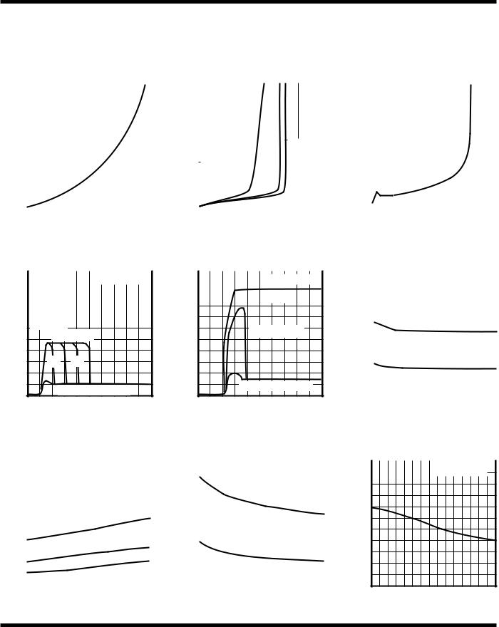
TYPICAL PERFORMANCE CHARACTERISTICS
TA = 25 ° C, unless otherwise specified.
OUTPUT VOLTAGE RESPONSE
(OFF→ ON)
|
CL = 2.2 µF |
|
CONT |
CN = 0.01 µF |
|
mV/DIV) |
||
V |
||
|
(5 |
|
|
OUT |
|
|
V |
|
OUT |
CN = 0.1 µF |
|
V |
ILOAD = 30 mA |
|
|
0 |
200 |
400 |
600 |
800 |
|
|
TIME (µs) |
|
|
LOAD REGULATION |
SHORT CIRCUIT CURRENT |
|
|
|
|
5 |
|
|
|
VOUT(TYP) |
|
|
4 |
|
|
|
|
|
|
|
|
|
|
|
|
(V) |
3 |
|
|
|
|
|
OUT |
|
|
|
|
|
|
|
|
|
|
|
|
|
V |
2 |
|
|
|
|
|
|
|
|
|
|
|
|
|
1 |
|
|
0 |
50 |
100 |
|
0 |
150 |
300 |
|
0 |
|||||
|
IOUT (mA) |
|
|
|
IOUT (mA) |
|
OUTPUT VOLTAGE VS. INPUT
VOLTAGE
|
|
VOUT(TYP) |
mV/DIV) |
IOUT = 0 mA |
|
|
IOUT = 30 mA |
|
(25 |
|
|
|
|
|
OUT |
|
IOUT = 50 mA |
|
|
|
V |
|
IOUT = 90 mA |
|
|
|
|
0 |
VIN = VOUT |
VIN (V) (50 mV/DIV)
|
DROPOUT VOLTAGE VS. |
LINE REGULATION |
OUTPUT CURRENT |
|
VOUT(TYP) |
|
|
0 |
|
|
mV/DIV)(50 |
|
|
DROP |
-100 |
|
|
|
|
|
(mV) |
|
|
|
|
|
|
-200 |
|
|
|
|
|
|
|
|
|
|
OUT |
|
|
V |
-300 |
|
|
|
|
|
|
|
|
|
V |
|
|
|
|
|
|
|
|
|
|
-400 |
|
|
0 |
10 |
20 |
|
0 |
100 |
200 |
|
VIN (V) |
|
|
|
IOUT (mA) |
|
October 1999 TOKO, Inc. |
Page 7 |
TK112xxB
TYPICAL PERFORMANCE CHARACTERISTICS (CONT.)
TA = 25 ° C, unless otherwise specified.
|
|
|
GROUND CURRENT VS. OUTPUT |
|
|
|
|
|
REVERSE BIAS CURRENT |
|
|
|
||||||||||||||||||||||||||||||||
|
|
|
|
|
|
|
|
|
|
(VIN = 0 V) |
|
|
|
|||||||||||||||||||||||||||||||
|
|
|
|
|
|
CURRENT |
|
|
|
|
|
|
|
|
|
|
|
|
|
|
||||||||||||||||||||||||
|
10 |
|
|
|
|
|
|
|
|
|
|
|
|
|
|
|
|
|
|
|
|
500 |
|
|
|
|
|
|
|
|
|
|
|
|
|
|
|
|
|
|
|
|
|
|
|
|
|
|
|
|
|
|
|
|
|
|
|
|
|
|
|
|
|
|
|
|
|
|
|
|
|
|
|
|
|
|
|
|
|
|
|
|
|
|
|
|
|||
|
|
|
|
|
|
|
|
|
|
|
|
|
|
|
|
|
|
|
|
|
|
|
|
|
|
|
|
|
|
|
|
|
|
|
|
|
|
|
|
|
||||
(mA) |
8 |
|
|
|
|
|
|
|
|
|
|
|
|
|
|
|
|
|
|
|
(µA) |
400 |
|
|
|
|
|
|
|
|
|
|
|
|
|
|
|
|
|
|
|
|
|
|
|
|
|
|
|
|
|
|
|
|
|
|
|
|
|
|
|
|
|
|
|
|
|
|
|
|
|
|
|
|
|
|
|
|
|
|
|
|
|
|
|
||||
|
|
|
|
|
|
|
|
|
|
|
|
|
|
|
|
|
|
|
|
|
|
|
|
|
|
|
|
|
|
|
|
|
|
|
|
|
|
|
|
|
||||
|
|
|
|
|
|
|
|
|
|
|
|
|
|
|
|
|
|
|
|
|
|
|
|
|
|
|
|
|
|
|
|
|
|
|
|
|
|
|
|
|||||
|
|
|
|
|
|
|
|
|
|
|
|
|
|
|
|
|
|
|
|
|
|
|
|
|
|
|
|
|
|
|
|
|
|
|
|
|
|
|
|
|
|
|||
|
|
|
|
|
|
|
|
|
|
|
|
|
|
|
|
|
|
|
|
|
|
|
|
|
|
|
|
|
|
|
|
|
|
|
|
|
|
|
|
|
|
|
||
6 |
|
|
|
|
|
|
|
|
|
|
|
|
|
|
|
|
|
|
|
300 |
|
|
|
|
|
|
|
|
|
1.9 V |
|
UPPER |
|
|
|
|
|
|||||||
GND |
|
|
|
|
|
|
|
|
|
|
|
|
|
|
|
|
|
|
|
|
REV |
|
|
|
|
|
|
|
|
|
|
|
|
|
|
|
|
|
|
|
||||
|
|
|
|
|
|
|
|
|
|
|
|
|
|
|
|
|
|
|
|
|
|
|
|
|
|
|
|
|
|
|
|
|
|
|
2.0 V |
|
|
|
|
|||||
|
|
|
|
|
|
|
|
|
|
|
|
|
|
|
|
|
|
|
|
|
|
|
|
|
|
|
|
|
|
|
|
|
|
|
|
|
|
|
||||||
|
4 |
|
|
|
|
|
|
|
|
|
|
|
|
|
|
|
|
|
|
|
I |
200 |
|
|
|
|
|
|
|
|
|
|
|
|
|
|
|
|
|
|
||||
|
|
|
|
|
|
|
|
|
|
|
|
|
|
|
|
|
|
|
|
|
|
|
|
|
||||||||||||||||||||
|
|
|
|
|
|
|
|
|
|
|
|
|
|
|
|
|
|
|
|
|
|
|
|
|
|
|
|
|
|
|
|
|
|
|
|
|
|
|
|
|
|
|||
I |
|
|
|
|
|
|
|
|
|
|
|
|
|
|
|
|
|
|
|
|
|
VOUT = 1.3 V |
|
|
|
|
|
|
|
|
|
|
|
|
|
|
|
|||||||
|
|
|
|
|
|
|
|
|
|
|
|
|
|
|
|
|
|
|
|
|
|
|
|
|
|
|
|
|
|
|
|
|
|
|
|
|
|
|||||||
|
2 |
|
|
|
|
|
|
|
|
|
|
|
|
|
|
|
|
|
|
|
|
100 |
|
|
|
|
|
|
|
|
|
|
|
|
|
|
|
|
|
|
|
|
|
|
|
|
|
|
|
|
|
|
|
|
|
|
|
|
|
|
|
|
|
|
|
|
|
|
|
|
|
|
|
|
|
|
|
|
|
|
|
|
|
|
|
|
|
||
|
|
|
|
|
|
|
|
|
|
|
|
|
|
|
|
|
|
|
|
|
|
|
|
|
|
|
|
|
|
|
|
|
|
|
|
|
|
|
|
|
|
|
||
|
|
|
|
|
|
|
|
|
|
|
|
|
|
|
|
|
|
|
|
|
|
|
|
|
|
|
|
|
|
|
|
|
|
|
|
|
|
|
|
|
|
|||
|
|
|
|
|
|
|
|
|
|
|
|
|
|
|
|
|
|
|
|
|
|
|
|
|
|
|
|
|
|
|
|
|
|
|
|
|
|
|
|
|
||||
|
|
|
|
|
|
|
|
|
|
|
|
|
|
|
|
|
|
|
|
|
|
|
|
|
|
|
|
|
|
|
|
|
|
|
|
|
|
|
|
|
|
|
|
|
|
0 |
|
|
|
|
|
|
|
|
|
|
|
|
|
|
|
|
|
|
|
|
0 |
|
|
|
|
|
|
|
|
|
|
|
|
|
|
|
|
|
|
|
|
|
|
|
|
|
|
|
|
|
|
|
|
|
|
|
|
|
|
|
|
|
|
|
|
|
|
|
|
|
|
|
|
|
|
|
|
|
|
|
|
|
|
|
|
|
||
|
|
|
|
|
|
|
|
|
|
|
|
|
|
|
|
|
|
|
|
|
|
|
|
|
|
|
|
|
|
|
|
|
|
|
|
|
|
|
|
|
|
|
||
|
|
|
|
|
|
|
|
|
|
|
|
|
|
|
|
|
|
|
|
|
0 |
10 |
|
|
|
|
|
|
|
|
20 |
|||||||||||||
|
0 |
100 |
|
|
|
|
|
|
|
|
200 |
|
|
|
|
|
|
|
|
|
||||||||||||||||||||||||
|
|
|
|
|
|
IOUT (mA) |
|
|
|
|
|
|
|
|
|
|
|
VREV (V) |
|
|
|
|||||||||||||||||||||||
|
|
|
|
QUIESCENT CURRENT (ON |
|
|
|
|
|
|
|
|
|
QUIESCENT CURRENT (ON |
|
|
|
|||||||||||||||||||||||||||
|
|
|
|
MODE) VS. INPUT VOLTAGE |
|
|
|
|
|
|
|
|
MODE) vs. INPUT VOLTAGE |
|
|
|
||||||||||||||||||||||||||||
|
|
|
|
|
|
|
|
|
|
|
|
|
|
|
|
|
|
|
|
|
|
|
|
|
|
|
|
|
|
|
|
|
|
|
|
|
|
|
||||||
|
2 |
|
|
|
|
|
|
|
|
IOUT = 0 mA |
|
|
1.0 |
|
|
|
|
|
|
|
|
|
|
|
|
IOUT = 0 mA |
|
|
|
|||||||||||||||
|
|
|
|
|
|
|
|
|
|
|
|
|
|
|
|
|
|
|
|
|
|
|
|
|
|
|
|
|
|
|
|
|
|
|
|
|
|
|
|
|
|
|
||
|
|
|
|
|
|
|
|
|
|
|
|
|
|
|
|
|
|
|
|
|
|
|
|
|
|
|
|
|
|
|
|
|
|
|
|
|
|
|
|
|||||
|
|
|
|
|
|
|
|
|
|
|
|
|
|
|
|
|
|
|
|
|
|
|
|
|
|
|
|
|
|
|
|
V |
OUT |
|
|
|
|
|||||||
|
|
|
|
|
|
|
|
|
|
|
|
|
|
|
|
|
|
|
|
|
|
|
|
|
|
|
|
|
|
|
|
|
|
|
|
|
|
|
|
|
|
|||
|
|
|
|
|
|
|
|
|
|
|
|
|
|
|
|
|
|
|
|
|
|
|
|
|
|
|
|
|
|
|
|
|
|
|
|
|
|
|
|
|
|
|
|
|
|
|
|
|
|
|
|
|
|
|
|
|
|
|
|
|
|
|
|
|
|
|
|
|
|
|
|
|
|
|
|
|
|
|
|
|
|
|
|
|
|
|
|
|
|
|
|
|
|
|
|
|
|
|
|
|
|
|
|
|
|
|
|
|
|
|
|
|
|
|
|
|
|
|
|
|
|
|
|
|
|
|
|
|
|
|
|
|
|
|
|
|
|
|
|
|
|
|
|
|
|
|
|
|
|
|
|
|
|
|
|
|
|
|
|
|
|
|
|
|
|
|
|
|
|
|
|
|
|
|
|
|
|
|
|
(mA) |
|
VOUT = |
|
|
(mA) |
|
VOUT = 1.9 V |
|
|
|
|
|
|
|
|
||
|
1 |
3 V |
5 V |
|
|
0.5 |
|
|
Q |
|
Q |
|
|
||||
|
|
|
|
|
|
|
||
I |
|
|
|
|
I |
|
|
|
|
|
2 V |
4 V |
|
|
|
|
|
|
0 |
VOUT = 1.3 to 1.8 V |
|
|
0 |
VOUT = 1.3 to 1.8 V |
|
|
|
|
|
|
|
||||
|
0 |
|
5 |
10 |
|
0 |
2.5 |
5 |
|
|
|
VIN (V) |
|
|
|
VIN (V) |
|
QUIESCENT CURRENT (OFF
MODE) VS. INPUT VOLTAGE
(pA) |
100 |
|
|
|
|
|
|
|
|
|
|
|
|
|
|
|
|
|
|
|
|
|
|
|
|
|
|
|
|
|
|
|
|
|
|
|
|
|
|
|
|
|
|
|
|
|
|
|
|
|
|
||
50 |
|
|
|
|
|
|
|
|
|
|
|
|
|
|
|
|
|
|
|
|
|
|
|
|
|
|
|
|
|
|
|
|
|
|
|
|
|
|
|
|
|
|
|
|
|
|
|
|
|
|
|
||
|
|
|
|
|
|
|
|
|
|
|
|
|
|
|
|
|
|
|
|
|
|
|
|
|
||
|
|
|
|
|
|
|
|
|
|
|
|
|
|
|
|
|
|
|
|
|
|
|
|
|
||
|
|
|
|
|
|
|
|
|
|
|
|
|
|
|
|
|
|
|
|
|
|
|
|
|
||
Q |
|
|
|
|
|
|
|
|
|
|
|
|
|
|
|
|
|
|
|
|
|
|
|
|
|
|
|
|
|
|
|
|
|
|
|
|
|
|
|
|
|
|
|
|
|
|
|
|
|
|
|
||
I |
|
|
|
|
|
|
|
|
|
|
|
|
|
|
|
|
|
|
|
|
|
|
|
|
|
|
|
0 |
|
|
|
|
|
|
|
|
|
|
|
|
|
|
|
|
|
|
|
|
|
|
|
|
|
|
|
|
|
|
|
|
|
|
|
|
|
|
|
|
|
|
|
|
|
|
|
|
|
|
|
|
|
|
|
|
|
|
|
|
|
|
|
|
|
|
|
|
|
|
|
|
|
|
|
|
|
|
|
|
|
|
|
|
|
|
|
|
|
|
|
|
|
|
|
|
|
|
|
|
|
|
|
|
|
|
|
|
|
|
|
|
|
|
|
|
|
|
|
|
|
|
|
|
|
|
|
|
|
|
|
|
|
|
|
|
|
10 |
|
|
|
|
|
|
|
|
|
|
20 |
|||||||||||
|
0 |
|
|
|
|
|
|
|
|
|
|
|
||||||||||||||
|
|
|
|
|
|
|
|
|
|
|
VIN (V) |
|
|
|
|
|
|
|
|
|
|
|
||||
|
|
|
|
|
|
|
GROUND CURRENT |
|
|
|
||||||||||||||||
|
2 |
|
|
|
|
|
|
|
|
|
|
|
|
|
|
|
|
|
|
|
|
|
|
|
|
|
|
|
|
|
|
|
|
|
|
|
|
|
|
|
|
|
|
|
|
|
|
|
|
|
|
|
|
|
|
|
|
|
|
|
|
|
|
|
|
|
|
|
|
|
|
|
|
|
|
|
|
|
|
|
|
|
|
|
|
|
|
|
|
|
|
|
|
|
|
|
|
|
|
|
|
|
|
|
|
||
|
|
|
|
|
|
|
|
|
|
|
|
|
|
|
|
|
|
|
|
|
|
|
|
|
|
|
(mA) |
|
|
|
|
|
|
IOUT = 60 mA |
|
|
|
|
|
|
|
|
|
|
|
||||||||
|
|
|
|
|
|
|
|
|
|
|
|
|
|
|
|
|
|
|
|
|
|
|
|
|
|
|
|
|
|
|
|
|
|
|
|
|
|
|
|
|
|
|
|
|
|
|
|
|
|
|
|
|
|
GND |
1 |
|
|
|
|
|
|
|
|
|
|
|
|
|
|
|
|
|
|
|
|
|
|
|
|
|
I |
|
|
|
|
|
|
|
|
|
|
|
|
|
|
|
|
|
|
|
|
|
|
|
|
|
|
|
|
|
|
|
|
|
|
|
|
|
|
|
|
|
|
|
|
|
|
|
|
|
|
|||
|
|
|
|
|
|
|
|
|
|
|
|
|
|
|
|
|
|
|
|
|
|
|
|
|
|
|
|
|
|
|
|
|
|
|
|
|
|
|
|
|
|
|
|
|
|
|
|
|
|
|
|
|
|
|
0 |
|
|
|
|
|
|
|
IOUT = 30 mA |
|
|
|
|
|
|
|||||||||||
|
|
|
|
|
|
|
|
|
|
|
|
|
|
|||||||||||||
|
|
|
|
|
|
|
|
|
|
|
|
|
|
|
|
|
|
|
|
|
|
|
|
|
|
|
|
-50 |
|
0 |
|
|
|
|
|
50 |
|
|
|
|
100 |
||||||||||||
|
|
|
|
|
|
|
|
|
|
|
TA (° C) |
|
|
|
|
|
|
|
|
|
|
|
||||
|
|
|
|
|
DROPOUT VOLTAGE |
|
|
|
|||||||||||||
|
500 |
|
|
|
|
|
|
|
|
|
|
|
|
|
|
|
|
|
|
|
|
|
|
|
|
|
|
|
|
|
|
|
|
|
|
|
|
|
|
|
|
|
|
|
|
|
|
|
|
|
|
|
|
|
|
|
|
|
|
|
|
|
|
|
|
(mV) |
400 |
|
|
|
|
|
|
|
|
|
|
|
|
|
|
|
|
|
|
|
|
|
|
|
|
|
|
|
|
|
|
|
|
|
|
|
|
|
|
|
|
||
|
|
|
|
|
|
|
|
|
|
|
|
|
|
|
|
|
|
|
|
||
|
|
|
|
|
|
|
|
|
|
|
|
|
|
|
|
|
|
|
|
|
|
300 |
|
|
|
|
|
|
|
|
IOUT = 150 mA |
|
|
|
|
||||||||
DROP |
|
|
|
|
|
|
|
|
|
|
|
|
|||||||||
|
|
|
|
|
|
|
|
|
|
|
|
|
|
|
|
|
|
|
|
||
|
|
|
|
|
|
|
|
|
|
|
|
|
|
|
|
|
|
|
|
|
|
|
|
|
|
|
|
|
|
|
|
|
|
|
|
|
|
|
|
|
|
|
|
200 |
|
|
|
|
|
|
|
|
|
IOUT = 60 mA |
|
|
|
||||||||
|
|
|
|
|
|
|
|
|
|
|
|
|
|||||||||
V |
100 |
|
|
|
|
|
|
|
|
|
|
|
|
|
|
|
|
|
|
|
|
|
|
|
|
|
|
|
|
|
|
|
|
|
|
|
|
|
|
|
|
|
|
|
|
|
|
|
|
|
|
|
|
|
|
|
|
|
|
|
|
|
|
|
|
|
|
|
|
|
|
|
|
|
|
|
|
|
|
|
|
|
|
|
|
|
|
|
|
|
|
|
|
|
|
|
|
|
|
|
|
|
|
|
|
|
|
|
|
|
0 |
|
|
|
|
|
|
|
|
|
|
IOUT = 30 mA |
|
|
|
||||||
|
|
|
|
|
|
|
|
|
|
|
|
|
|
||||||||
|
|
|
|
|
|
|
|
|
|
|
|
|
|
|
|
|
|
|
|
|
|
|
|
|
|
|
|
|
|
|
|
|
|
|
|
|
|
|
|
|
|
|
|
|
-50 |
0 |
50 |
|
|
|
|
100 |
|||||||||||||
|
|
|
|
|
|
|
|
TA (° C) |
|
|
|
||||||||||
ICONT (µA)
|
|
|
|
CONTROL CURRENT |
|
|
|
|
|
|||||||||
50 |
|
|
|
|
|
|
|
|
|
|
|
|
|
|
|
|
|
|
|
|
|
|
|
|
|
|
|
|
|
|
|
|
|
|
|
|
|
|
|
|
|
|
|
|
|
|
|
|
|
|
|
|
|
|
|
|
40 |
|
|
|
|
|
|
|
|
|
|
|
|
|
|
|
|
|
|
|
|
|
|
|
|
|
|
|
|
|
|
|
|
|
|
|
|
|
|
|
|
|
|
|
|
|
VCONT = 5 V |
|
|
|
|||||||
|
|
|
|
|
|
|
|
|
|
|
||||||||
30 |
|
|
|
|
|
|
|
|
|
|
|
|
|
|
|
|
|
|
|
|
|
|
|
|
|
|
|
|
|
|
|
|
|
|
|
|
|
|
|
|
|
|
|
|
|
|
|
|
|
|
|
|
|
|
|
|
20 |
|
|
|
|
|
|
|
|
|
|
|
|
|
|
|
|
|
|
|
|
|
|
|
|
|
|
|
|
|
|
|
|
|
|
|
|
|
|
|
|
|
|
|
|
|
|
|
|
|
|
|
|
|
|
|
|
10 |
|
|
|
|
|
|
|
|
VCONT = 1.8 V |
|
|
|||||||
|
|
|
|
|
|
|
|
|
|
|||||||||
|
|
|
|
|
|
|
|
|
|
|
|
|
|
|
|
|
|
|
|
|
|
|
|
|
|
|
|
|
|
|
|
|
|
|
|
|
|
0 |
|
|
|
|
|
|
|
|
|
|
|
|
|
|
|
|
|
|
|
|
|
|
|
|
|
|
|
|
|
|
|
|
|
|
|
|
|
|
0 |
50 |
|
|
|
|
|
|
|
|||||||||
-50 |
|
|
100 |
|||||||||||||||
|
|
|
|
|
|
|
TA (° C) |
|
|
|
|
|
||||||
VCONT (V)
|
VCONT (VOUT, ON POINT) |
|||||||||||||||
2.0 |
|
|
|
R |
|
CONT = 0 Ω |
|
|||||||||
|
|
|
|
|||||||||||||
1.0
0 -50 0 50 100
TA (° C)
Page 8 |
October 1999 TOKO, Inc. |
 Loading...