

TIANMA TM190MDS01 Specification
Global LCD Panel Exchange Center
www.panelook.com
SHANGHAI AVIC OPTOELECTRONICS co-Q/S1011-2011
MODEL NO. : TM190MDS01
ISSUED DATE: 2011/08/28
VERSION : 1.2
ƑPreliminary Specification
ŶFinal Product Specification
Customer :
Approved by Notes
SHANGHAI AVIC Confirmed :
Prepared by Checked by Approved by
This technical specification is subjected to change without notice
The information contained herein is the exclusive property of SHANGHAI AVIC OPTOELECTRONICS
Corporation, and shall not be distributed, reproduced, or disclosed in whole or in part without prior written
permission of SHANGHAI AVIC OPTOELECTRONICS Corporation.
One step solution for LCD / PDP / OLED panel application: Datasheet, inventory and accessory!
Page 1 of 35
www.panelook.com

Global LCD Panel Exchange Center
www.panelook.com
SHANGHAI AVIC OPTOELECTRONICS co-Q/S1011-2011
TABLE OF CONTENTS
TABLE OF CONTENTS ............................................................................................................................................................. 2
RECORD
1.
OUTLINE
1.1 STRUCTURE AND PRINCIPLE
1.2 APPLICATIONS
1.3 FEATURES
2.
GENERAL SPECIFICATIONS
3.
ABSOLUTE MAXIMUM RATINGS
4.
BLOCK DIAGRAM
5.
MECHANICAL SPECIFICATIONS
6.
ELECTRICAL CHARACTERISTICS
6.1 DRIVING FOR LCD
6.2 DRIVING FOR BACKLIGHT
7.
CONNECTIONS AND FUNCTIONS FOR INTERFACE PINS
7.1 LVDS
7.2 BACKLIGHT
7.3 POSITION OF PLUGS AND A SOCKET
7.4 CONNECTION BETWEEN RECEIVER AND TRANSMITTER FOR LVDS
8.
DISPLAY COLORS AND INPUT DATA SIGNALS
9.
INTERFACE TIMING
9.1 TIMING CHARACTERISTICS
9.2 INPUT SIGNAL TIMING CHART
9.3 PIXEL DATA ALIGNMENT OF DISPLAY IMAGE
9.4. POWER SUPPLY VOLTAGE SEQUENCE
10. OPTICS
11.
12.
12.1 PRODUCT LABEL
12.2 INDICATION LOCATIONS
13.
14.
15.OUTDRAWING
OF REVISION
RELIABILITYTESTS
MARKINGS
PACKING, TRANSPORTATION AND DELIVERY
PRECAUTIONS
......................................................................................................................................................... 3
............................................................................................................................................................................. 4
.......................................................................................................................... 4
................................................................................................................................................... 4
.......................................................................................................................................................... 4
............................................................................................................................................ 5
................................................................................................................................... 6
............................................................................................................................................................. 7
.................................................................................................................................... 8
.................................................................................................................................. 9
............................................................................................................................................. 9
.............................................................................................................................. 10
........................................................................................ 11
.................................................................................................................................................................. 11
....................................................................................................................................................... 12
........................................................................................................... 12
...................................................... 13
.......................................................................................................... 14
........................................................................................................................................................ 16
........................................................................................................................... 16
..................................................................................................................... 17
............................................................................................ 18
....................................................................................................... 19
.............................................................................................................................................................. 21
...................................................................................................................................................... 25
...................................................................................................................................................................... 27
........................................................................................................................................... 27
............................................................................................................................... 28
........................................................................................................ 29
............................................................................................................................................................... 31
................................................................................................................................................................ 34
The information contained herein is the exclusive property of SHANGHAI AVIC OPTOELECTRONICS
Corporation, and shall not be distributed, reproduced, or disclosed in whole or in part without prior written
permission of SHANGHAI AVIC OPTOELECTRONICS Corporation.
One step solution for LCD / PDP / OLED panel application: Datasheet, inventory and accessory!
Page 2 of 35
www.panelook.com

Global LCD Panel Exchange Center
www.panelook.com
SHANGHAI AVIC OPTOELECTRONICS co-Q/S1011-2011
RECORD OF REVISION
Rev Issued Date Description Editor
1.0 2010-9-20 Preliminary Release Stephen Sun
1.1 2011-03-07 Final Spec. Release wei zhang
1.2 2011-08-28
LED Connecter 2Pin-6Pin ; Light bar
operation voltage change; Add Reliability test
Chunjie xiao
The information contained herein is the exclusive property of SHANGHAI AVIC OPTOELECTRONICS
Corporation, and shall not be distributed, reproduced, or disclosed in whole or in part without prior written
permission of SHANGHAI AVIC OPTOELECTRONICS Corporation.
One step solution for LCD / PDP / OLED panel application: Datasheet, inventory and accessory!
Page 3 of 35
www.panelook.com

Global LCD Panel Exchange Center
www.panelook.com
SHANGHAI AVIC OPTOELECTRONICS co-Q/S1011-2011
1. OUTLINE
1.1 STRUCTURE AND PRINCIPLE
TM190MDS01-00 module is composed of the amorphous silicon thin film transistor liquid crystal
display (a-Si TFT LCD) panel structure with driver LSIs for driving the TFT (Thin Film Transistor) array and a
backlight. The a-Si TFT LCD panel structure is injected liquid crystal material into a narrow gap between the
TFT array glass substrate and a color-filter glass substrate.
Color (Red, Green, Blue) data signals from a host system (e.g. PC, signal generator, etc.) are
modulated into best form for active matrix system by a signal processing board, and sent to the driver LSIs
which drive the individual TFT arrays. The TFT array as an electro-optical switch regulates the amount of
transmitted light from the backlight assembly, when it is controlled by data signals. Color images are created
by regulating the amount of transmitted light through the TFT array of red, green and blue dots.
1.2 APPLICATIONS
• Monitor for PC
1.3 FEATURES
• a-Si TFT active matrix
• LVDS interface
• R.G.B input 8bit, 16.7 millions colors (6bit+Hi-FRC)
• Resolution WXGA+ (1,440× 900 pixels)
• Wide viewing angle 85°/85° (L/R); 80°/80° (U/D)
• High contrast ratio 1000 :1
• Module size 428.0 (H) ×278.0 (V) ×9.8 (D) mm
• Fast response time (Ton+ Toff= 5 ms˅
• High gamut (68%)
• Edge light type backlight (White-LED)
• Inverter less
• RoHS compliance
• TCO5.0 compliance
The information contained herein is the exclusive property of SHANGHAI AVIC OPTOELECTRONICS
Corporation, and shall not be distributed, reproduced, or disclosed in whole or in part without prior written
permission of SHANGHAI AVIC OPTOELECTRONICS Corporation.
One step solution for LCD / PDP / OLED panel application: Datasheet, inventory and accessory!
Page 4 of 35
www.panelook.com

Global LCD Panel Exchange Center
www.panelook.com
SHANGHAI AVIC OPTOELECTRONICS co-Q/S1011-2011
2. GENERAL SPECIFICATIONS
Display area 408.24 (H) × 255.15 (V) mm (typ.)
Diagonal size of display 48.1 cm
Drive system a-Si TFT active matrix
Display color 16.7 M colors (6bit+ Hi-FRC)
Pixel 1,440 (H) × 900(V) pixels
Pixel arrangement
Dot pitch 0.0945 (H) × 0.2835(V) mm
Pixel pitch 0.2835 (H) × 0.2835 (V) mm
Module size
Weight
Contrast ratio
RGB vertical stripe
428.0 (H) ×278.0 (V) ×9.8 (D) mm
1700 g˄max.˅
1000 :1 (typ.)
Viewing angle
Color gamut
Response time
Luminance
Transmissive Mode
Surface Treatment
Signal system
Power supply voltage LCD panel signal processing board: 5.0V
Backlight White-LED
Power consumption
170°/ 160° (typ.)
68 % (typ.)
5 ms (typ.)
250 cd/m
Normally White
Anti Glare
LVDS 2port
13W˄Typ.˅
2
(typ.)
The information contained herein is the exclusive property of SHANGHAI AVIC OPTOELECTRONICS
Corporation, and shall not be distributed, reproduced, or disclosed in whole or in part without prior written
permission of SHANGHAI AVIC OPTOELECTRONICS Corporation.
One step solution for LCD / PDP / OLED panel application: Datasheet, inventory and accessory!
Page 5 of 35
www.panelook.com
Global LCD Panel Exchange Center
ć
˄ˁRH˅
www.panelook.com
SHANGHAI AVIC OPTOELECTRONICS co-Q/S1011-2011
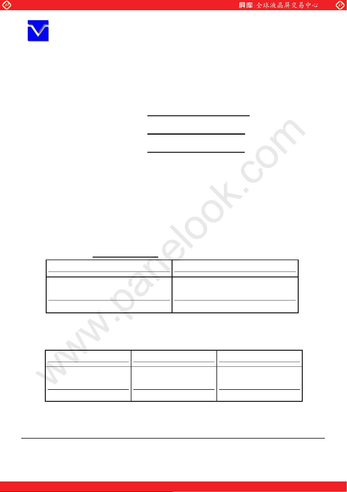
3. ABSOLUTE MAXIMUM RATINGS
Parameter Symbol Rating Unit Remarks
Power
supply
voltage
Power voltage
Light bar voltage V 43.2
Input voltage for signals Vi -0.3 ~ +3.3 V Ta = 25°C
Light bar peak forward current I 400
Storage temperature Tst -20 ~ +60 °C Note 4
Operating temperature Top 0 ~ +50 °C Note 4, 5
Absolute humidity AH g/m Ta > 50°C
Operating altitude - 4,850 m 0°C Ta 50°C
Storage altitude - 13,600 m -20°C Ta 60°C
Note1: Display signals are DA0+/-, DA1+/-, DA2+/-, DA3+/-, CKA+/-, DB0+/-, DB1+/-, DB2+/-, DB3+/-,
and CKB+/-.
Note2: Function signal is MSL.
Note3: Pulse widthPVHFDQGGXW\
Note4: Temperature and relative humidity range is shown in the figure below.
(a) 90%RH Max. (Ta 40°C)
(b) Wet-bulb temperature should be39°C Max. (Ta> 40°C)
(c) No condensation.
Note5: The temperature of panel display surface area should be 0°C Min and 60°C Max.
VDD -0.3 ~ +6.0 V Ta = 25°C
LED
F
Vrms Ta = 25°C
mArms Note 3
3
Relative Humidity
80
60
Operating Range
40
20
Temperature (
)
5
Storage Range
-40 -20 0 20 40 60 80
The information contained herein is the exclusive property of SHANGHAI AVIC OPTOELECTRONICS
Corporation, and shall not be distributed, reproduced, or disclosed in whole or in part without prior written
permission of SHANGHAI AVIC OPTOELECTRONICS Corporation.
Page 6 of 35
One step solution for LCD / PDP / OLED panel application: Datasheet, inventory and accessory!
www.panelook.com
Global LCD Panel Exchange Center
www.panelook.com
SHANGHAI AVIC OPTOELECTRONICS co-Q/S1011-2011
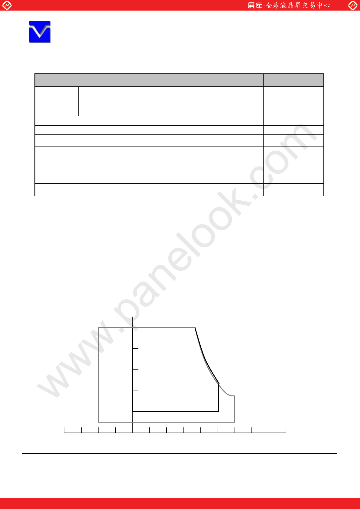
4. BLOCK DIAGRAM
I/F
DA0+
DA0-
DA1+
DA1-
DA2+
DA2-
CKA+
CKA-
DA3+
DA3-
DB0+
DB0-
DB1+
DB1-
DB2+
DB2-
CKB+
CKA-
DB3+
DB3-
LCD MODULE
100ȍ
100ȍ
100ȍ
100ȍ
100ȍ
100ȍ
100ȍ
100ȍ
100ȍ
100ȍ
LVDS Receiver
Timing Controller
Source Driver
Gate Driver
LCD Panel
H: 1440× 3˄R,G,B˅
V: 900
VDD
DC/DC
Power
Edge side backlight
`
V
1/2
LED
FG
GND
Note: System ground (GND), FG (Frame ground) in the product should be connected together in
customer equipment.
The information contained herein is the exclusive property of SHANGHAI AVIC OPTOELECTRONICS
Corporation, and shall not be distributed, reproduced, or disclosed in whole or in part without prior written
permission of SHANGHAI AVIC OPTOELECTRONICS Corporation.
Page 7 of 35
One step solution for LCD / PDP / OLED panel application: Datasheet, inventory and accessory!
www.panelook.com

Global LCD Panel Exchange Center
www.panelook.com
SHANGHAI AVIC OPTOELECTRONICS co-Q/S1011-2011
5. MECHANICAL SPECIFICATIONS
Parameter Specification Unit
Module size 428.0± 0.5 (W) × 278.0 ± 0.5 (H) × 9.8 ± 0.5 (D) mm
Display area 408.24(H) × 255.15(V) mm (typ.), [48.1 cm] mm
Weight
1700˄max.˅
g
The information contained herein is the exclusive property of SHANGHAI AVIC OPTOELECTRONICS
Corporation, and shall not be distributed, reproduced, or disclosed in whole or in part without prior written
permission of SHANGHAI AVIC OPTOELECTRONICS Corporation.
One step solution for LCD / PDP / OLED panel application: Datasheet, inventory and accessory!
Page 8 of 35
www.panelook.com

Global LCD Panel Exchange Center
5V
www.panelook.com
SHANGHAI AVIC OPTOELECTRONICS co-Q/S1011-2011
6. ELECTRICAL CHARACTERISTICS
6.1 DRIVING FOR LCD
Parameter Symbol min. typ. max. Unit Remarks
Power supply voltage VDD 4.5 5.0 5.5 V -
Power supply current IDD -
700
Note1
Permissible ripple voltage VRP - - 200 mV VDD
Differential input voltage
Differential input threshold
voltage for LVDS receiver
Low VTL -100 - - mV
High VTH - - 100 mV
Input voltage width for LVDS
receiver
ΊVidΊ
Vi 0 - 3.3 V -
200 600 mV
Terminating resistor RT - 100 - ȍ -
Rush current I -
rush
- 3.0 A Note4
1000
Note 2
mA at VDD = 5.0V
at VCM = 1.2V
Note3
Note 1: Black pattern
Note 2: 1H1V dot inverse pattern
Note 3: Common mode voltage for LVDS receiver
Note4:
Measurement Conditions:
R1
47K
S2
GND
5V
1
2
3
SW- SP DT
12V
Q1
MOSFET- N
R2
1K
R3
20K
C3
Cap
10uF/16V
C2
Cap
1uF/16V
Q2
MOSFET- N
GND
F1
Fuse ( 2 A)
GND
C1
Cap
1uF/16V
VDD
The information contained herein is the exclusive property of SHANGHAI AVIC OPTOELECTRONICS
Corporation, and shall not be distributed, reproduced, or disclosed in whole or in part without prior written
permission of SHANGHAI AVIC OPTOELECTRONICS Corporation.
One step solution for LCD / PDP / OLED panel application: Datasheet, inventory and accessory!
Page 9 of 35
www.panelook.com
Global LCD Panel Exchange Center
www.panelook.com
SHANGHAI AVIC OPTOELECTRONICS co-Q/S1011-2011
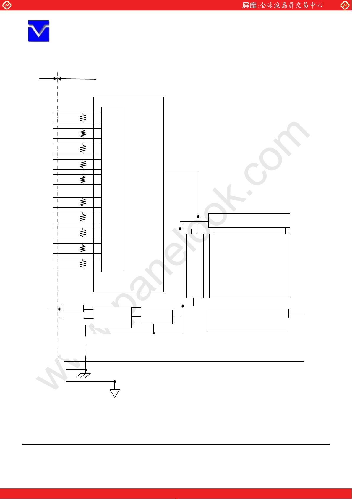
6.2 DRIVING FOR BACKLIGHT
(Ta=25°C) Note1
Parameter
Light bar operation
voltage
(for reference)
Light bar operation
current
Light bar operating
lifetime
Note1: The backlight of this product is made up of 1 light bar, LED to be 4014, 40pieces, 10 serials and 4
parallels.
Note2: The light bar can work normally if the PWM dimming ratio range is from 0% to 100% and the
operation current is 240mA.
Note3: The operating lifetime is mean time to half-luminance. In case the product works under room
temperature environment.
Symbo
l
V28
LED
I -
LED
min. typ. max. Unit Remarks
31 35 Vrms
240 - mArms
Hr - 30000 - Hour I
Operating with fixed
driving current
Pin No1; Pin No2;
Pin No5;Pin No6˗
for 60mArms
=240mA,Note3
LED
The information contained herein is the exclusive property of SHANGHAI AVIC OPTOELECTRONICS
Corporation, and shall not be distributed, reproduced, or disclosed in whole or in part without prior written
permission of SHANGHAI AVIC OPTOELECTRONICS Corporation.
One step solution for LCD / PDP / OLED panel application: Datasheet, inventory and accessory!
Page 10 of 35
www.panelook.com
Global LCD Panel Exchange Center
www.panelook.com
SHANGHAI AVIC OPTOELECTRONICS co-Q/S1011-2011
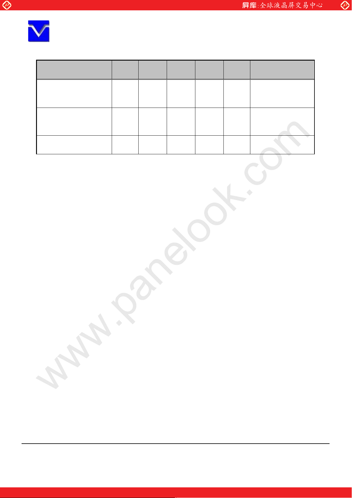
7. CONNECTIONS AND FUNCTIONS FOR INTERFACE PINS
7.1 LVDS
CN1: FI-XB30SSRLA-HF16 (Produced by JAE) or equivalent.
Pin Name Description
1 RXO0- Negative LVDS differential data input. Channel O0 (odd)
2 RXO0+ Positive LVDS differential data input. Channel O0 (odd)
3 RXO1- Negative LVDS differential data input. Channel O1 (odd)
4 RXO1+ Positive LVDS differential data input. Channel O1 (odd)
5 RXO2- Negative LVDS differential data input. Channel O2 (odd)
6 RXO2+ Positive LVDS differential data input. Channel O2 (odd)
7 GND Ground
8 RXOC- Negative LVDS differential clock input. (odd)
9 RXOC+ Positive LVDS differential clock input. (odd)
10 RXO3- Negative LVDS differential data input. Channel O3(odd)
11 RXO3+ Positive LVDS differential data input. Channel O3 (odd)
12 RXE0- Negative LVDS differential data input. Channel E0 (even)
13 RXE0+ Positive LVDS differential data input. Channel E0 (even)
14 GND Ground
15 RXE1- Negative LVDS differential data input. Channel E1 (even)
16 RXE1+ Positive LVDS differential data input. Channel E1 (even)
17 GND Ground
18 RXE2- Negative LVDS differential data input. Channel E2 (even)
19 RXE2+ Positive LVDS differential data input. Channel E2 (even)
20 RXEC- Negative LVDS differential clock input. (even)
21 RXEC+ Positive LVDS differential clock input. (even)
22 RXE3- Negative LVDS differential data input. Channel E3 (even)
23 RXE3+ Positive LVDS differential data input. Channel E3 (even)
24 GND Ground
25 GND Ground
26 NC Not connection.
27 GND Ground
28 VCC +5.0V power supply
29 VCC +5.0V power supply
30 VCC +5.0V power supply
The information contained herein is the exclusive property of SHANGHAI AVIC OPTOELECTRONICS
Corporation, and shall not be distributed, reproduced, or disclosed in whole or in part without prior written
permission of SHANGHAI AVIC OPTOELECTRONICS Corporation.
One step solution for LCD / PDP / OLED panel application: Datasheet, inventory and accessory!
Page 11 of 35
www.panelook.com
 Loading...