


TDA2040
20W Hi-Fi AUDIO POWER AMPLIFIER
DESCRIPTION
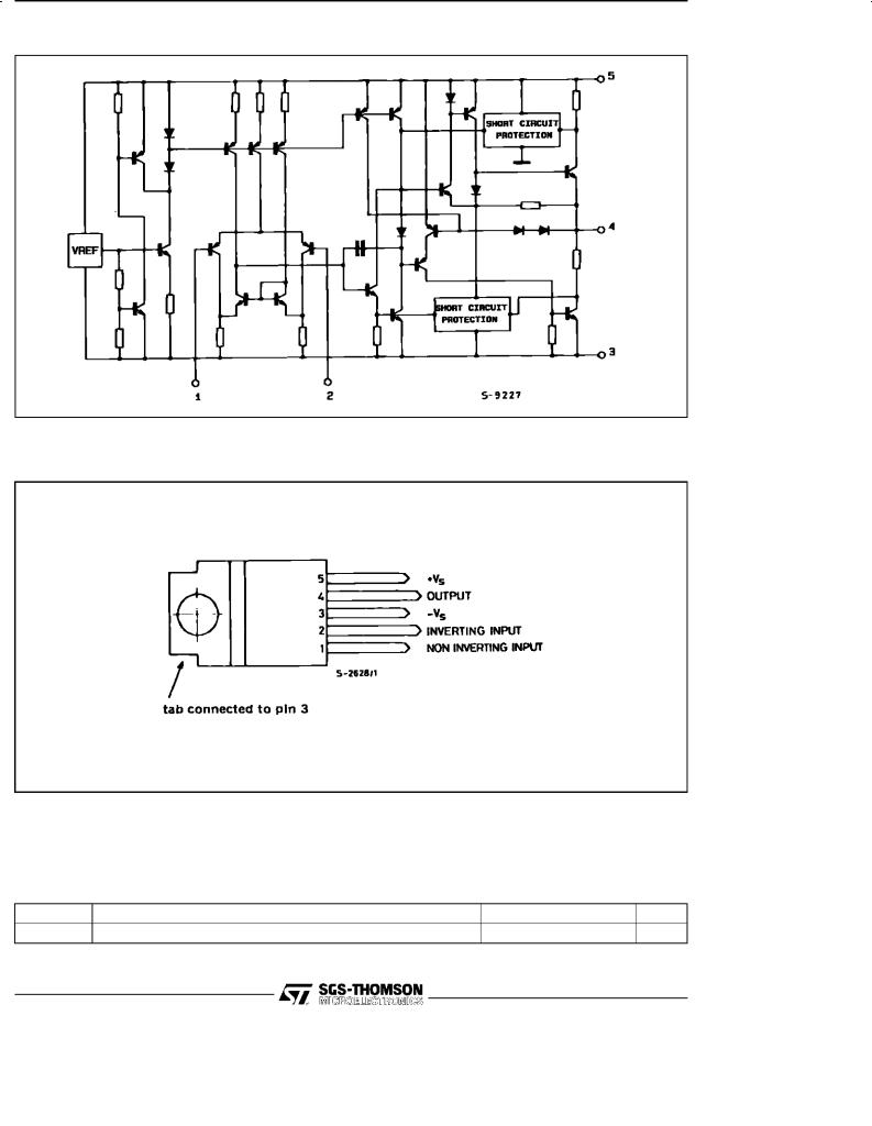
The TDA2040 is a monolithic integrated circuit in Pentawatt package,intended for use as an audio class AB amplifier. Typically it provides 22W output power (d = 0.5%) at Vs = 32V/4Ω . The TDA2040 provides high output current and has very low harmonic and cross-over distortion. Further the device incorporates a patented short circuit protection system comprising an arrangement for automaticallylimiting the dissipated power so as to keep the working point of the output transistors within their safe operating area. A thermal shut-down system is also included.
PENTAWATT
ORDERING NUMBER : TDA2040V
TEST CIRCUIT
December 1995 |
1/13 |
TDA2040
SCHEMATIC DIAGRAM
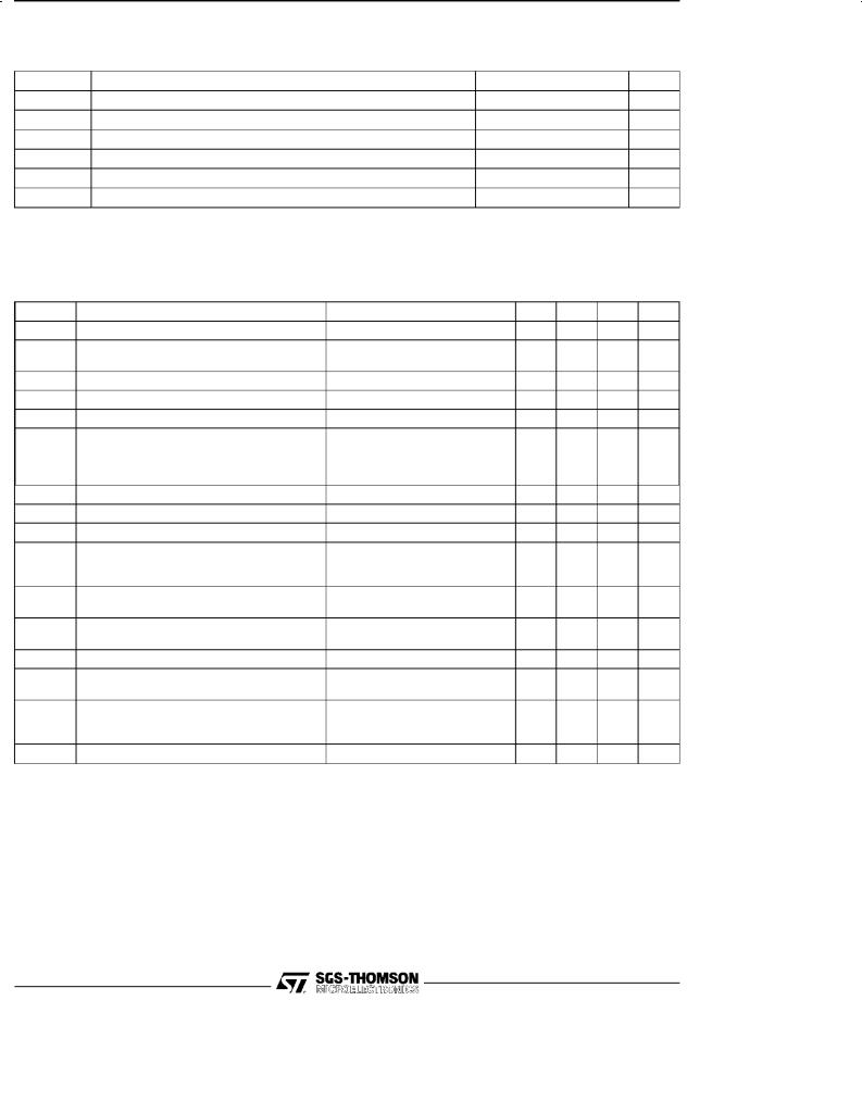
PIN CONNECTION
THERMAL DATA
Symbol |
Parameter |
|
Value |
Unit |
Rth j-case |
Thermal Resistance Junction-case |
Max. |
3 |
°C/W |
2/13
|
|
|
TDA2040 |
ABSOLUTE MAXIMUM RATINGS |
|
|
|
Symbol |
Parameter |
Value |
Unit |
Vs |
Supply Voltage |
± 20 |
V |
Vi |
Input Voltage |
Vs |
|
Vi |
Differential Input Voltage |
± 15 |
V |
Io |
Output Peak Current (internally limited) |
4 |
A |
Ptot |
Power Dissipation at Tcase = 75 °C |
25 |
W |
Tstg, Tj |
Storage and Junction Temperature |
± 40 to + 150 |
°C |
ELECTRICAL CHARACTERISTICS
(refer to the test circuit, VS = ± 16V, Tamb = 25oC unless otherwise specified)
Symbol |
Parameter |
Test Conditions |
Min. |
Typ. |
Max. |
Unit |
|
Vs |
Supply Voltage |
|
|
± 2.5 |
|
± 20 |
V |
Id |
Quiescent Drain Current |
Vs = ± 4.5V |
|
|
|
30 |
mA |
|
|
Vs = ± 20V |
|
|
45 |
100 |
mA |
Ib |
Input Bias Current |
Vs = ± 20V |
|
|
0.3 |
1 |
μA |
Vos |
Input Offset Voltage |
Vs = ± 20V |
|
|
± 2 |
± 20 |
mV |
Ios |
Input Offset Current |
|
|
|
|
± 200 |
nA |
Po |
Output Power |
d = 0.5%, Tcase = 60°C |
|
|
|
W |
|
|
|
f = 1kHz |
RL = 4Ω |
20 |
22 |
|
|
|
|
|
RL = 8Ω |
|
12 |
|
|
|
|
f = 15kHz |
RL = 4Ω |
15 |
18 |
|
|
BW |
Power Bandwidth |
Po = 1W, RL = 4Ω |
|
100 |
|
kHz |
|
Gv |
Open Loop Voltage Gain |
f = 1kHz |
|
|
80 |
|
dB |
Gv |
Closed Loop Voltage Gain |
f = 1kHz |
|
29.5 |
30 |
30.5 |
dB |
d |
Total Harmonic Distortion |
Po = 0.1 to 10W, RL = 4Ω |
|
0.08 |
|
% |
|
|
|
f = 40 to 15000Hz |
|
|
|
||
|
|
f = 1kHz |
|
|
0.03 |
|
|
eN |
Input Noise Voltage |
B = Curve A |
|
|
2 |
|
μV |
|
|
B = 22Hz to 22kHz |
|
3 |
10 |
μV |
|
iN |
Input Noise Current |
B = Curve A |
|
|
50 |
|
pA |
|
|
B = 22Hz to 22kHz |
|
80 |
200 |
|
|
Ri |
Input Resistance (pin 1) |
|
|
0.5 |
5 |
|
MΩ |
SVR |
Supply Voltage Rejection |
RL = 4Ω, Rg = 22kΩ, Gv = 30dB |
40 |
50 |
|
dB |
|
|
|
f = 100Hz, Vripple = 0.5VRMS |
|
|
|
|
|
η |
Efficiency |
f = 1kHz |
RL = 8 Ω |
|
66 |
|
% |
|
|
Po = 12W |
|
|
|
||
|
|
Po = 22W |
RL = 4 Ω |
|
63 |
|
|
Tj |
Thermal Shut-down Junction Temperature |
|
|
|
145 |
|
°C |
3/13

TDA2040
Figure 1 : Output Power versus Supply Voltage |
Figure 2 : Output Power versus Supply Voltage |
Figure 3 : Output Power versus Supply Voltage |
Figure 4 : Distortion versus Frequency |
Figure 5 : Supply Voltage Rejection versus |
Figure 6 : Supply Voltage Rejection versus |
Frequency |
Voltage Gain |
4/13
 Loading...