

Page 1

User's Guide
SNAU228–January 2018
USB2ANY Interface Adapter
This user's guide describes the USB2ANY Interface Adapter and its general setup and operation.
Contents
1 Introduction ................................................................................................................... 2
1.1 How to Use This Manual........................................................................................... 2
1.2 Information About Cautions and Warnings...................................................................... 2
1.3 FCC Warning........................................................................................................ 3
1.4 Description........................................................................................................... 3
2 Overview of Hardware Design ............................................................................................. 4
3 Connecting the USB2ANY.................................................................................................. 7
3.1 Using the 10-Pin Cable ............................................................................................ 8
3.2 Using the 30-Pin Cable ............................................................................................ 8
3.3 Connecting the USB2ANY to the Computer .................................................................... 9
3.4 Connecting the USB2ANY to an EVM ........................................................................... 9
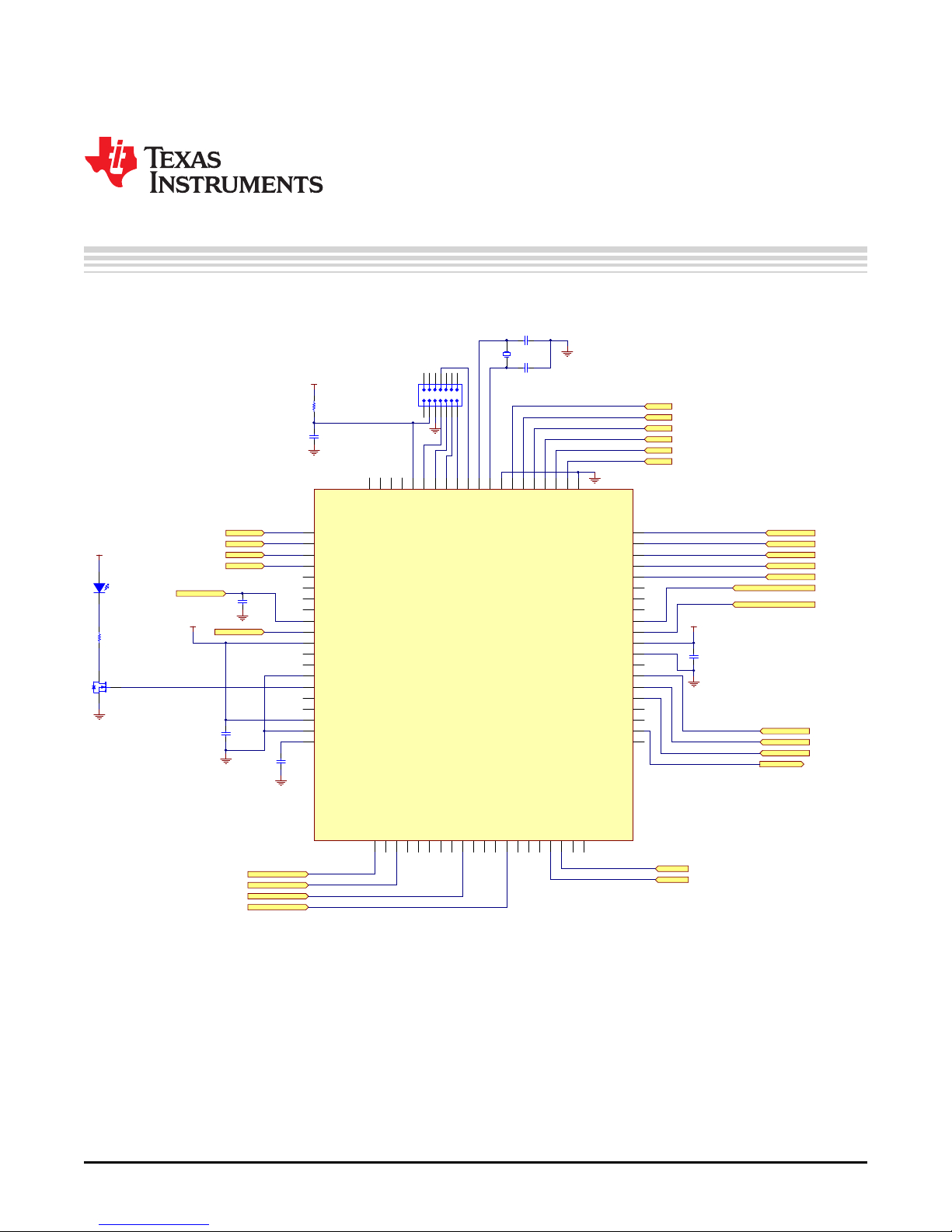
Appendix A USB2ANY Schematic............................................................................................. 10
Appendix B USB2ANY Cable Connections................................................................................... 13
List of Figures
1 USB2ANY and the Supplied Cables ...................................................................................... 3
2 USB2ANY Block Diagram .................................................................................................. 5
3 USB2ANY PCB .............................................................................................................. 6
4 10-Pin Cable With Key...................................................................................................... 7
5 10-pin Cable Connection ................................................................................................... 8
6 30-Pin Cable Connection ................................................................................................... 8
7 USB Connector .............................................................................................................. 9
SNAU228–January 2018
Submit Documentation Feedback
Copyright © 2018, Texas Instruments Incorporated
USB2ANY Interface Adapter
1
Page 2

Introduction
8 Connection Between the USB2ANY and the EVM...................................................................... 9
9 USB2ANY Schematic 1 ................................................................................................... 10
10 USB2ANY Schematic 2 ................................................................................................... 11
11 USB2ANY Schematic 3 ................................................................................................... 12
12 USB2ANY Interface Connectors ......................................................................................... 13
13 10-Pin IDC Cable Connector ............................................................................................. 14
14 10-Pin IDC Cable Detail................................................................................................... 14
15 30-Pin IDC Cable Connector ............................................................................................. 15
16 30-Pin IDC Cable Detail ................................................................................................... 15
1 Status LEDs .................................................................................................................. 6
2 10-pin Cable Pinouts....................................................................................................... 14
3 30-pin Cable Pinouts....................................................................................................... 15
Trademarks
All trademarks are the property of their respective owners.
1 Introduction
1.1 How to Use This Manual
This document contains the following chapters:
• Chapter 1 – Introduction
• Chapter 2 – Overview of Hardware Design
• Chapter 3 – Connecting the USB2ANY
• Appendices
www.ti.com
List of Tables
1.2 Information About Cautions and Warnings
The EVM contains components that can potentially be damaged by electrostatic
discharge. Always transport and store the EVM in the supplied ESD bag, when
not in use. Handle using an antistatic wristband. Operate on an antistatic work
surface. For more information on proper handling, refer to Electrostatic
Discharge (ESD).
Due to the limited use and location of use (antistatic professional laboratory or other controlled
environment) the equipment under test (EUT) will not see an ESD event above 2 kV, and was tested
accordingly. Manufacturer’s specifications in the manual include this limitation.
CAUTION
2
USB2ANY Interface Adapter
Copyright © 2018, Texas Instruments Incorporated
SNAU228–January 2018
Submit Documentation Feedback
Page 3

www.ti.com
1.3 FCC Warning
This equipment is intended for use in a laboratory test environment only. The equipment generates, uses,
and can radiate radio frequency energy and has not been tested for compliance with the limits of
computing devices pursuant to subpart J of part 15 of FCC rules, which are designed to provide
reasonable protection against radio frequency interference. Operation of this equipment in other
environments may cause interference with radio communications, in which case, the user, at their own
expense, is required to take whatever measures may be required to correct this interference.
1.4 Description
The USB2ANY is a small dongle intended to allow a computer to control an electronic evaluation module
(EVM) via a USB connection. These EVMs cannot normally connect directly to the computer because of
their specialized interfaces, which are typically supported on commercial computers.
The USB2ANY is a USB 2.0 device supporting several different interfaces, including:
• 13 general purpose input/output (GPIO) (shared) lines with switchable pullup or pulldown resistors
• I2C with programmable 1.5-kΩ pullup resistors
• SPI – up to 8-MHz SCLK
• UART (300 to 230,400 Baud)
• Four analog inputs, 12-bit analog-to-digital converter (ADC)
• Two analog outputs, 8-bit digital-to-analog converter (DAC)
• Four PWM outputs
• Several other interfaces
• Switchable 3.3-V or 5-V power to DUT
The USB2ANY board can source regulated 3.3-V and 5.0-V DC power to the target device, up to a
maximum of 300 mA (combined 3.3 V and 5.0 V). The voltage outputs have built-in current sensing and
limiting circuits that protect both the EVM and the USB2ANY from overcurrent, shorts, and so forth.
The USB2ANY is shipped with a USB cable, a 10-pin cable (for most common interfaces), and a 30-pin
cable (for all supported interfaces).
Introduction
Figure 1. USB2ANY and the Supplied Cables
SNAU228–January 2018
Submit Documentation Feedback
Copyright © 2018, Texas Instruments Incorporated
USB2ANY Interface Adapter
3
Page 4

Overview of Hardware Design
2 Overview of Hardware Design
The USB2ANY is based on TI’s MSP430F5529 microcontroller, which has the following features making it
ideal for a multi-interface controller:
• 16-bit RISC CPU
• Operates at 3.3 V
• 128KB flash memory
• 10KB SRAM
• 63 I/O pins
• Fast execution (25-MHz clock)
• Four 16-bit counters and timers
• Two universal serial communication interfaces (supports SPI, I2C, UART)
• Full-speed universal serial bus (USB) with internal PHY supporting USB 2.0
• 12-bit ADC
• Hardware multiplier supporting 32-bit operations
• Three-channel internal DMA
See Appendix A: USB2ANY Schematic for schematic drawings.
The block diagram in Figure 2 shows the fundamental parts of the USB2ANY:
1. USB connector – The USB connector connects to the host computer. The USB2ANY is a
USB 2.0 full-speed device using a HID-class driver. The board has a Mini-USB connector installed.
2. Power Management – The power management circuitry allows the application program to turn the
+3.3-V or the +5.0-V external power outputs on or off. It also detects power faults (for example,
overload or short circuit) and notifies the application program.
3. MSP430F5529 – This MSP430 microcontroller communicates with the application program and
executes the received API function commands. It is programmed with the USB2ANY firmware, which
controls all of the interface peripherals and other necessary functions (for example, timing, scheduling,
encoding and decoding data).
4. DAC1, DAC2 – These are the DAC outputs. Under program control, these outputs can source a
voltage from 0 V to 3.3 V, in 256 steps.
5. GPIO – These GPIO signals are used to read/write single-bit digital signals. When used as inputs, they
can optionally be programmed to be pulled up, pulled down, or floating (MOS input with no resistor).
6. I2C – The inter-integrated circuit interface is an industry-standard serial interface often used to
communicate between devices in a closed system. I2C requires two signal wires plus a ground
connection. The I2C interface of the USB2ANY uses a 7-bit address, which allows the bus to support
up to 127 devices.
7. SPI – The industry-standard serial peripheral interface is generally faster than I2C, but more difficult to
implement. It is often used to communicate between devices in a closed system. SPI usually requires
four signal wires plus a ground connection, but can use as few as three wires or as many as needed to
select among the number of devices connected to the bus. While there is no real limit as to the
maximum number of devices on a SPI bus, the number is usually limited by practical issues like fanout, cable length, signaling speed, and capacitive loading.
8. PWM – The pulse-width modulated outputs allow the USB2ANY to produced pulse trains with variable
frequency and duty cycle. This can be used for clocks, integrators (such as those used in PWM servo
motors), tone generation, and so forth.
9. Analog Inputs – The USB2ANY has four analog inputs. Two of the inputs (ADC0, ADC1) have no
external amplifiers (effectively unity gain) and the other two inputs (ADC2, ADC3) have a gain of two.
The gain allows smaller signals to be amplified slightly, giving them a larger scale at the ADC inputs.
The MSP430F5529 utilizes 12-bit ADCs, giving a full-scale digital value of 4095.
10. Ext. V
ADCs. By default, V
– The external voltage reference allows selection of the voltage used as the reference by the
REF
is set to use AVCC, which is physically connected to VCC(3.3-V nominal).
REF
www.ti.com
4
USB2ANY Interface Adapter
Copyright © 2018, Texas Instruments Incorporated
SNAU228–January 2018
Submit Documentation Feedback
Page 5

Power Management
(14)
MSP430F5529
Switchable
1
2C pullups
(4)
+3.3 V
+5.0 V
DAC1
DAC2
GPIO, 12C, PWM,
and other interfaces
(shared lines)
Analog Inputs
Ext. V
REF
Copyright © 2017, Texas Instruments Incorporated
www.ti.com
Overview of Hardware Design
Figure 2. USB2ANY Block Diagram
Figure 3 shows the USB2ANY PCB without the enclosure. One end has three interface connectors that
are typically connected to an EVM (J3, J4, and J5). Connectors J3 and J5 have eight pins and J4 has 10
pins. Most applications will use only J4 because it provides access to the most commonly used interfaces
(see Using the 10-Pin Cable in Connecting the USB2ANY). Alternatively, a 30-pin cable is provided that
connects to all three connectors (J3, J4, and J5) and provides access to all available interface signals.
SNAU228–January 2018
Submit Documentation Feedback
Copyright © 2018, Texas Instruments Incorporated
USB2ANY Interface Adapter
5
Page 6

Overview of Hardware Design
www.ti.com
Figure 3. USB2ANY PCB
The Status LED indicates the status of the electronics and firmware, as follows:
Table 1. Status LEDs
LED State Meaning
OFF No power to the board. USB cable may be unplugged.
ON Power is applied and the board is operating normally.
Blinking A hardware, firmware, or USB error occurred. Board must be power-cycled.
NOTE: The LED may also be programmed using the software API to be ON, OFF, or blinking. In
that case, the LED may not indicate the actual status of the electronics or firmware.
Switch S1 is used to put the firmware into bootstrap loader (BSL) mode. The BSL mode is used to load or
update the USB2ANY firmware and is entered whenever the board is powered-up while Switch S1 is
depressed.
The USB Mini-B (J2) connector is used to connect the USB2ANY to the host computer. A cable with a
USB Mini-B connector on one end and a USB A connector on the other end is provided with the
USB2ANY.
The JTAG connector (J1) is used only for firmware development and is normally not populated with a
physical connector.
6
USB2ANY Interface Adapter
Copyright © 2018, Texas Instruments Incorporated
SNAU228–January 2018
Submit Documentation Feedback
Page 7

www.ti.com
3 Connecting the USB2ANY
NOTE: This section assumes you are using the USB2ANY in its gray plastic enclosure (as shown in
Figure 1). If the USB2ANY board has been removed from the enclosure, or the board came
without an enclosure, some interpretation and adjustments may need to be made in these
instructions.
The USB2ANY ships with two cables, one 10-pin and one 30-pin. Both cables are standard 0.050-in (1.25mm) pitch ribbon cables with IDC-type connectors. The connectors have a key to assure that they are
installed correctly.
Connecting the USB2ANY
Figure 4. 10-Pin Cable With Key
NOTE: If you are using the USB2ANY board without its enclosure, the key must face away from the
PCB. Be sure to carefully align the male pins on the PCB with the cable connector.
SNAU228–January 2018
Submit Documentation Feedback
Copyright © 2018, Texas Instruments Incorporated
USB2ANY Interface Adapter
7
Page 8

or
or
Connecting the USB2ANY
3.1 Using the 10-Pin Cable
The 10-pin cable is connected to J4 as Figure 5 shows and can be used for most of the popular
interfaces, including:
• I2C: SDA and SCL
• SPI: SCLK, MOSI, MISO, and CS
• UART: RX and TX
• Power: 3.3-V external
• GPIO: GPIO0, GPIO1, GPIO2, GPIO3, GPIO4, GPIO5, GPIO6, and GPIO7
• PWM: PWM0, PWM1, and PWM2
• OneWire: OW1, OW2, and OW3
• µWire: SCLK, MOSI, MISO, and CS
• RFFE: SCLK and SDATA
www.ti.com
Figure 5. 10-pin Cable Connection
3.2 Using the 30-Pin Cable
The 30-pin cable is connected across J3, J4, and J5 as Figure 6 shows, and can be used to access all of
the available interfaces signals (see Table 2 for a list of all the signals).
8
USB2ANY Interface Adapter
Figure 6. 30-Pin Cable Connection
Copyright © 2018, Texas Instruments Incorporated
SNAU228–January 2018
Submit Documentation Feedback
Page 9

www.ti.com
3.3 Connecting the USB2ANY to the Computer
The USB2ANY has a USB Mini-B connector on the right side. Plug the provided USB cable (or any USB
cable with a Mini-B connector) into the USB2ANY. Plug the other end of the cable (USB ‘A’) into the
computer.
Figure 7. USB Connector
Connecting the USB2ANY
When connected, the LED on the USB2ANY should flicker quickly a few times, and then stay on.
3.4 Connecting the USB2ANY to an EVM
Depending on the EVM, choose either the 10-pin ribbon cable or the 30-pin ribbon cable. The majority of
EVMs use the 10-pin version, as Figure 8 shows.
Figure 8. Connection Between the USB2ANY and the EVM
SNAU228–January 2018
Submit Documentation Feedback
Copyright © 2018, Texas Instruments Incorporated
USB2ANY Interface Adapter
9
Page 10
P6.4/CB4/A4
1
P6.5/CB5/A5
2
P6.6/CB6/A6
3
P6.7/CB7/A7
4
P7.0/CB8/A12
5
P7.1/CB9/A13
6
P7.2/CB10/A14
7
P7.3/CB11/A15
8
P5.0/A8/VREF+ /VeREF+
9
P5.1/A9/VREF-/V eREF-
10
AVCC1
11
P5.4/XIN
12
P5.4/XOUT
13
AVSS1
14
P8.0
15
P8.1
16
P8.2
17
DVCC1
18
DVSS1
19
VCORE
20
P1.0/TA0CLK/ACLK21P1.1/TA0.022P1.2/TA0.123P1.3/TA0.224P1.4/TA0.325P1.5/TA0.426P1.6/TA1CLK/CBOUT27P1.7/TA1.028P2.0/TA1.129P2.1/TA1.230P2.2/TA2CLK/SMCLK31P2.3/TA2.032P2.4/TA2.133P2.5/TA2.234P2.6/RTCCLK/DMAE035P2.7/UCB0STE/UCA0CLK36P3.0/UCB0SIMO/UCB0SDA37P3.1/UCB0SOMI/UCB0SCL38P3.2/UCB0CLK/UCA0STE39P3,3/UCA0TXD/UCA0SIM
40
P3.4/UCA0RXD/UCA0S OMI
41
P3.5/TB0.5
42
P3.6/TB0.6
43
P3.7/TB0OUTH/SV MOUT
44
P4.0PM_UCB1STE/ PM_UCA1CLK
45
P4.1/PM_UCB1SIM O/PM_UCB1SDA
46
P4.2/PM_UCB1SOMI /PM_UCB1SCL
47
P4.3/PM_UCB1CLK/ PM_UCA1STE
48
DVSS2
49
DVCC2
50
P4.4/PM_UCA1TXD/PM_UCA1SIMO
51
P4.5/PM_UCA1RXD/PM_UCA1S OMI
52
P4.6/PM_NONE
53
P4.7/PM_NONE
54
P5.6/TB0.0
55
P5.7/TB0.1
56
P7.4/TB0.2
57
P7.5/TB0.3
58
P7.6/TB0.4
59
P7.7/TB0CLK/MCLK
60
VSSU
61
PU.0/DP
62
PUR
63
PU.1/DM
64
VBUS65VUSB
66
V18
67
AVSS2
68
P5.2/XT2IN
69
P5.3/XT2OUT
70
TEST/SBWTCK
71
PJ.0/TDO
72
PJ.1/TDI/TCLK
73
PJ.2/TMS
74
PJ.3/TCK
75
/RST/NMI/SBWTDIO
76
P6.0/CB0/A077P6.1/CB1/A178P6.2/CB2/A279P6.3/CB3/A3
80
U1
MSP430F5529IPNR
+3.3V
GPIO11/VEREF+
GPIO10/VEREF-
+3.3V
GND
+3.3V
GND
DP
PUR
DM
VBUS
VUSB
V18
GPIO1/I2C(SCL)
GPIO0/I2C(SDA)
GPIO7/PWM0
GPIO6/PWM1/SPI(CS)
GPIO3/PWM2
SDABR D
SCLBRD
+3.3V
GPIO2/SPI(SCLK)
GPIO5/SPI(SOMI)/UA RT(RXD)
GPIO4/SPI(SIMO)/U ART(TXD)
PWM3
I2CPU
EXT5V_EN
EXT5V_FAULT
EXT3.3V_EN
EXT3.3V_FAULT
EFC0/GPIO12/CLOCK
AIN_B_0
AIN_B_1
GPIO9/ADC2
GPIO8/ADC3
30pF
C1
30pF
C2
2200pF
C3
GND
33k
R1
0.1µF
C5
0.1µF
C4
GND
0.1µF
C6
GND
GND
GND
GND
GND
200
R2
1 2
3 4
5 6
7 8
9 10
11 12
13 14
J1
1 2
Y1
0.47µF
C7
1
2 3
50V
Q1
D1
SSF-LXH305GD-TR
Copyright © 2017, Texas Instruments Incorporated
USB2ANY Schematic
Figure 9, Figure 10, and Figure 11 illustrate the USB2ANY schematics.
Appendix A
SNAU228–January 2018
Figure 9. USB2ANY Schematic 1
10
USB2ANY Schematic
Copyright © 2018, Texas Instruments Incorporated
SNAU228–January 2018
Submit Documentation Feedback
Page 11

+3.3VGND
GND
GND
GND
GND
GND
ADC1
ADC0
AIN_B_0
AIN_B_1
GND
+3.3V
GND
GND
GND
+3.3V
DAC1
DAC0
SCLBRD
SDABRD
GND
+3.3V
VBUS
DM
DP
PUR
VUSB
V18
+3.3V
GND
GND
GND
220pF
C16
GND
GND
1.5k
R14
1.5k
R15
0.1µF
C17
0.1µF
C18
0.
1µF
C20
0.
15µF
C19
1.00k
R16
1.00k
R19
390
R21
39
0
R18
D
AC5571IDBV
VOUT
1
GND
2
VDD3SDA
4
SCL
5
A0
6
U8
S1
EVQ-PSD02K
2
3
4
1
5
J2
33k
R8
33
R4
33
R6
1.5k
1.07Meg
R22
220pF
C10
1.00k
R20
0
.15µF
C21
1
.00k
R17
IO1
1
IO2
2
GND
3
IO3
4
IO4
5
VCC
6
U3
TPD4E004DRYR
10µF
C9
DAC5571IDBV
VOUT
1
GND
2
VDD3SDA
4
SCL
5
A0
6
U6
1
3
2
4 8
U7A
TLV2442AIDR
7
5
6
4 8
U7B
TLV2442AIDR
Copyright © 2017, Texas Instruments Incorporated
www.ti.com
Appendix A
SNAU228–January 2018
Submit Documentation Feedback
Figure 10. USB2ANY Schematic 2
Copyright © 2018, Texas Instruments Incorporated
USB2ANY Schematic
11
Page 12

TPS2553-1
IN
1
GND
2
EN3~FAULT
4
ILIM
5
OUT
6
U2
GND
GND
GND
GND
GND
GND
GND GND
GND
GND
+3.3V
GND
GND
GND
EXT5V_FAULT
EXT3.3V_FAULT
EXT5V_EN
EXT3.3V_EN
VBUS
GND
GND
GPIO0/I2C(SDA)
GPIO1/I2C(SCL)
GND
I2CPU
GND
DAC0
+5V_EXT
PWM3
DAC1
EFC0/GPIO12/CLOCK
GPIO2/SPI(SCLK)
GPIO3/PWM2
+3.3V_EXT
GPIO4/SPI(SIMO)/U ART(TXD) GPIO5/SPI(SOMI)/UA RT(RXD)
GPIO6/PWM1/SPI(CS) GPIO7/PWM0
GPIO10/VEREF- GPIO11/VEREF+
GPIO8/ADC3 GPIO9/ADC2
ADC1 ADC0
GND
GND
X1 X2 X3 X4
1µF
C8
1µF
C11
130k
R3
100k
R5
100k
R11
1.5k
R12
1.5k
R13
TP1
TPS2553-1
IN
1
GND
2
EN3~FAULT
4
ILIM
5
OUT
6
U5
+3.3V_EXT
+5V_EXT
+5V_EXT
+3.3V_EXT
+3.3V_EXT
1 2
3 4
5 6
7 8
J5
1 2
3 4
5 6
7 8
9 10
J4
1 2
3 4
5 6
7 8
J3
12V
Q2
12V
Q4
1
2 3
60V
Q3
TP2 TP3
7.5V
2 1
D2
1SMB5922BT3G
22µF
C13
90 ohm
FB1
OUT
1
NC
2
NR/FB
3
GND
4
EN
5
NC
6
NC
7
IN
8
PWPD
9
U4
TPS73533DRB
0.01µF
C15
2.2µF
C12
TP4
100k
R10
160k
R9
1µF
C14
TP5
Copyright © 2016, Texas Instruments Incorporated
Appendix A
www.ti.com
Figure 11. USB2ANY Schematic 3
12
USB2ANY Schematic
Copyright © 2018, Texas Instruments Incorporated
SNAU228–January 2018
Submit Documentation Feedback
Page 13

Appendix B
SNAU228–January 2018
USB2ANY Cable Connections
The USB2ANY has four interface connectors: one USB 2.0 connector (J2) and three I/O connectors (J3,
J4, and J5). The USB connector is a standard ‘A’ type mini USB receptacle. The I/O connectors are
standard dual-row, 0.1-in center, pin headers.
I/O connectors J3 and J5 are 8-pin type and J4 is a 10-pin type. They are configured such that they will
accept either individual cable connections or a single 30-pin connection.
Figure 12. USB2ANY Interface Connectors
The standard USB2ANY kit (HPA665-001) includes both a 10-pin cable and a 30-pin cable. The 10-pin
cable is intended to be connected to J4. This single connection will supply the needs for many users as it
provides access to the following interfaces and signals:
• I2C: SDA and SCL
• SPI: SCLK, MOSI, MISO, and CS
• UART: RX and TX
• Power: 3.3 V External
• GPIO: GPIO0, GPIO1, GPIO2, GPIO3, GPIO4, GPIO5, GPIO6, and GPIO7
• PWM: PWM0, PWM1, and PWM2
• OneWire: OW1, OW2, and OW3
• μWire: SCLK, MOSI, MISO, and CS
• RFFE: SCLK and SDATA
SNAU228–January 2018
Submit Documentation Feedback
Copyright © 2018, Texas Instruments Incorporated
USB2ANY Cable Connections
13
Page 14

Appendix B
• Interrupts: INT0, INT1, and INT2
The 10-pin cable is about 6 in long and has a keyed female 10-pin IDC connector on each end. Connect
the cable to the USB2ANY board as Figure 13 shows (note that the key must be facing up, away from the
board).
www.ti.com
Figure 13. 10-Pin IDC Cable Connector
The opposite end of the cable is intended to be connected to the EVM or other target device. The red
stripe on the cable indicates pin 1.
Figure 14. 10-Pin IDC Cable Detail
Table 2. 10-pin Cable Pinouts
Schematic Pin Number Cable Pin Number Signals Available
J4-10 1 GPIO7, PWM0, INT2, OW2, OW5
J4-9 2 GPIO6, PWM1, RFFE:SCLK, SPI:CS, INT1, µWIRE:CS, OW1
J4-8 3 GPIO5, SPI:SOMI, UART:RXD, µWIRE:SOMI
J4-7 4 GPIO4, SPI:SIMO, UART:TXD, µWIRE:SIMO
J4-6 5 3.3VEXT
J4-5 6 GND
J4-4 7 GPIO3, PWM2, RFFE:SDATA, INT0
J4-3 8 GPIO2, ES:DOUT, SPI:SCLK, µWIRE:SCLK
14
USB2ANY Cable Connections
SNAU228–January 2018
Submit Documentation Feedback
Copyright © 2018, Texas Instruments Incorporated
Page 15
www.ti.com
The 30-pin cable is also about 6 inches in length and has a keyed female 30-pin IDC connector on each
end. This cable provides access to all available signals. The cable should be connected to the USB2ANY
board as Figure 15 shows (note that the key must be facing up, away from the board).
Appendix B
Table 2. 10-pin Cable Pinouts (continued)
Schematic Pin Number Cable Pin Number Signals Available
J4-2 9 GPIO1, I2C:SCL, OW3
J4-1 10 GPIO0, I2C:SDA, OW4
NOTE: The pin numbers for J4 on the schematics are for reference only and do not correspond to
the pin numbers for cable connections.
Figure 15. 30-Pin IDC Cable Connector
Connect the opposite end of the cable to the EVM or other target device. The red stripe on the cable
indicates pin 1.
Figure 16. 30-Pin IDC Cable Detail
Table 3. 30-pin Cable Pinouts
Schematic Pin Number Cable Pin Number Signals Available
J3-8 1 DAC0
J3-7 2 PIO12, CLOCK, EFC0, INT3
J3-6 3 +5VEXT
SNAU228–January 2018
Submit Documentation Feedback
Copyright © 2018, Texas Instruments Incorporated
USB2ANY Cable Connections
15
Page 16

Appendix B
www.ti.com
Table 3. 30-pin Cable Pinouts (continued)
Schematic Pin Number Cable Pin Number Signals Available
J3-5 4 GND
J3-4 5 PWM3
J3-3 6 GND
J3-2 7 DAC1
J3-1 8 GND
— 9 (unused)
— 10 (unused)
J4-10 11 GPIO7, PWM0, INT2, OW2, OW5
J4-9 12 GPIO6, PWM1, RFFE:SCLK, SPI:CS, INT1, µWIRE:CS, OW1
J4-8 13 GPIO5, SPI:SOMI, UART:RXD, µWIRE:SOMI
J4-7 14 GPIO4, SPI:SIMO, UART:TXD, µWIRE:SIMO
J4-6 15 3.3VEXT
J4-5 16 GND
J4-4 17 GPIO3, PWM2, RFFE:SDATA, INT0
J4-3 18 GPIO2, ES:DOUT, SPI:SCLK, µWIRE:SCLK
J4-2 19 GPIO1, I2C:SCL, OW3
J4-1 20 GPIO0, I2C:SDA, OW4
— 21 (unused)
— 22 (unused)
J5-8 23 ADC0
J5-7 24 ADC1
J5-6 25 GPIO9, ADC2, ES:AIN
J5-5 26 GPIO8, ADC3
J5-4 27 GND
J5-3 28 GND
J5-2 29 GPIO11, VREF+
J5-1 30 GPIO10, VREF–
NOTE: The pin numbers for J3, J4, and J5 on the schematics are for reference only and do not
correspond to the pin numbers for cable connections.
16
USB2ANY Cable Connections
Copyright © 2018, Texas Instruments Incorporated
SNAU228–January 2018
Submit Documentation Feedback
Page 17

STANDARD TERMS FOR EVALUATION MODULES
1. Delivery: TI delivers TI evaluation boards, kits, or modules, including any accompanying demonstration software, components, and/or
documentation which may be provided together or separately (collectively, an “EVM” or “EVMs”) to the User (“User”) in accordance
with the terms set forth herein. User's acceptance of the EVM is expressly subject to the following terms.
1.1 EVMs are intended solely for product or software developers for use in a research and development setting to facilitate feasibility
evaluation, experimentation, or scientific analysis of TI semiconductors products. EVMs have no direct function and are not
finished products. EVMs shall not be directly or indirectly assembled as a part or subassembly in any finished product. For
clarification, any software or software tools provided with the EVM (“Software”) shall not be subject to the terms and conditions
set forth herein but rather shall be subject to the applicable terms that accompany such Software
1.2 EVMs are not intended for consumer or household use. EVMs may not be sold, sublicensed, leased, rented, loaned, assigned,
or otherwise distributed for commercial purposes by Users, in whole or in part, or used in any finished product or production
system.
2 Limited Warranty and Related Remedies/Disclaimers:
2.1 These terms do not apply to Software. The warranty, if any, for Software is covered in the applicable Software License
Agreement.
2.2 TI warrants that the TI EVM will conform to TI's published specifications for ninety (90) days after the date TI delivers such EVM
to User. Notwithstanding the foregoing, TI shall not be liable for a nonconforming EVM if (a) the nonconformity was caused by
neglect, misuse or mistreatment by an entity other than TI, including improper installation or testing, or for any EVMs that have
been altered or modified in any way by an entity other than TI, (b) the nonconformity resulted from User's design, specifications
or instructions for such EVMs or improper system design, or (c) User has not paid on time. Testing and other quality control
techniques are used to the extent TI deems necessary. TI does not test all parameters of each EVM.
User's claims against TI under this Section 2 are void if User fails to notify TI of any apparent defects in the EVMs within ten (10)
business days after delivery, or of any hidden defects with ten (10) business days after the defect has been detected.
2.3 TI's sole liability shall be at its option to repair or replace EVMs that fail to conform to the warranty set forth above, or credit
User's account for such EVM. TI's liability under this warranty shall be limited to EVMs that are returned during the warranty
period to the address designated by TI and that are determined by TI not to conform to such warranty. If TI elects to repair or
replace such EVM, TI shall have a reasonable time to repair such EVM or provide replacements. Repaired EVMs shall be
warranted for the remainder of the original warranty period. Replaced EVMs shall be warranted for a new full ninety (90) day
warranty period.
3 Regulatory Notices:
3.1 United States
3.1.1 Notice applicable to EVMs not FCC-Approved:
FCC NOTICE: This kit is designed to allow product developers to evaluate electronic components, circuitry, or software
associated with the kit to determine whether to incorporate such items in a finished product and software developers to write
software applications for use with the end product. This kit is not a finished product and when assembled may not be resold or
otherwise marketed unless all required FCC equipment authorizations are first obtained. Operation is subject to the condition
that this product not cause harmful interference to licensed radio stations and that this product accept harmful interference.
Unless the assembled kit is designed to operate under part 15, part 18 or part 95 of this chapter, the operator of the kit must
operate under the authority of an FCC license holder or must secure an experimental authorization under part 5 of this chapter.
3.1.2 For EVMs annotated as FCC – FEDERAL COMMUNICATIONS COMMISSION Part 15 Compliant:
CAUTION
This device complies with part 15 of the FCC Rules. Operation is subject to the following two conditions: (1) This device may not
cause harmful interference, and (2) this device must accept any interference received, including interference that may cause
undesired operation.
Changes or modifications not expressly approved by the party responsible for compliance could void the user's authority to
operate the equipment.
FCC Interference Statement for Class A EVM devices
NOTE: This equipment has been tested and found to comply with the limits for a Class A digital device, pursuant to part 15 of
the FCC Rules. These limits are designed to provide reasonable protection against harmful interference when the equipment is
operated in a commercial environment. This equipment generates, uses, and can radiate radio frequency energy and, if not
installed and used in accordance with the instruction manual, may cause harmful interference to radio communications.
Operation of this equipment in a residential area is likely to cause harmful interference in which case the user will be required to
correct the interference at his own expense.
Page 18

FCC Interference Statement for Class B EVM devices
NOTE: This equipment has been tested and found to comply with the limits for a Class B digital device, pursuant to part 15 of
the FCC Rules. These limits are designed to provide reasonable protection against harmful interference in a residential
installation. This equipment generates, uses and can radiate radio frequency energy and, if not installed and used in accordance
with the instructions, may cause harmful interference to radio communications. However, there is no guarantee that interference
will not occur in a particular installation. If this equipment does cause harmful interference to radio or television reception, which
can be determined by turning the equipment off and on, the user is encouraged to try to correct the interference by one or more
of the following measures:
• Reorient or relocate the receiving antenna.
• Increase the separation between the equipment and receiver.
• Connect the equipment into an outlet on a circuit different from that to which the receiver is connected.
• Consult the dealer or an experienced radio/TV technician for help.
3.2 Canada
3.2.1 For EVMs issued with an Industry Canada Certificate of Conformance to RSS-210 or RSS-247
Concerning EVMs Including Radio Transmitters:
This device complies with Industry Canada license-exempt RSSs. Operation is subject to the following two conditions:
(1) this device may not cause interference, and (2) this device must accept any interference, including interference that may
cause undesired operation of the device.
Concernant les EVMs avec appareils radio:
Le présent appareil est conforme aux CNR d'Industrie Canada applicables aux appareils radio exempts de licence. L'exploitation
est autorisée aux deux conditions suivantes: (1) l'appareil ne doit pas produire de brouillage, et (2) l'utilisateur de l'appareil doit
accepter tout brouillage radioélectrique subi, même si le brouillage est susceptible d'en compromettre le fonctionnement.
Concerning EVMs Including Detachable Antennas:
Under Industry Canada regulations, this radio transmitter may only operate using an antenna of a type and maximum (or lesser)
gain approved for the transmitter by Industry Canada. To reduce potential radio interference to other users, the antenna type
and its gain should be so chosen that the equivalent isotropically radiated power (e.i.r.p.) is not more than that necessary for
successful communication. This radio transmitter has been approved by Industry Canada to operate with the antenna types
listed in the user guide with the maximum permissible gain and required antenna impedance for each antenna type indicated.
Antenna types not included in this list, having a gain greater than the maximum gain indicated for that type, are strictly prohibited
for use with this device.
Concernant les EVMs avec antennes détachables
Conformément à la réglementation d'Industrie Canada, le présent émetteur radio peut fonctionner avec une antenne d'un type et
d'un gain maximal (ou inférieur) approuvé pour l'émetteur par Industrie Canada. Dans le but de réduire les risques de brouillage
radioélectrique à l'intention des autres utilisateurs, il faut choisir le type d'antenne et son gain de sorte que la puissance isotrope
rayonnée équivalente (p.i.r.e.) ne dépasse pas l'intensité nécessaire à l'établissement d'une communication satisfaisante. Le
présent émetteur radio a été approuvé par Industrie Canada pour fonctionner avec les types d'antenne énumérés dans le
manuel d’usage et ayant un gain admissible maximal et l'impédance requise pour chaque type d'antenne. Les types d'antenne
non inclus dans cette liste, ou dont le gain est supérieur au gain maximal indiqué, sont strictement interdits pour l'exploitation de
l'émetteur
3.3 Japan
3.3.1 Notice for EVMs delivered in Japan: Please see http://www.tij.co.jp/lsds/ti_ja/general/eStore/notice_01.page 日本国内に
輸入される評価用キット、ボードについては、次のところをご覧ください。
http://www.tij.co.jp/lsds/ti_ja/general/eStore/notice_01.page
3.3.2 Notice for Users of EVMs Considered “Radio Frequency Products” in Japan: EVMs entering Japan may not be certified
by TI as conforming to Technical Regulations of Radio Law of Japan.
If User uses EVMs in Japan, not certified to Technical Regulations of Radio Law of Japan, User is required to follow the
instructions set forth by Radio Law of Japan, which includes, but is not limited to, the instructions below with respect to EVMs
(which for the avoidance of doubt are stated strictly for convenience and should be verified by User):
1. Use EVMs in a shielded room or any other test facility as defined in the notification #173 issued by Ministry of Internal
Affairs and Communications on March 28, 2006, based on Sub-section 1.1 of Article 6 of the Ministry’s Rule for
Enforcement of Radio Law of Japan,
2. Use EVMs only after User obtains the license of Test Radio Station as provided in Radio Law of Japan with respect to
EVMs, or
3. Use of EVMs only after User obtains the Technical Regulations Conformity Certification as provided in Radio Law of Japan
with respect to EVMs. Also, do not transfer EVMs, unless User gives the same notice above to the transferee. Please note
that if User does not follow the instructions above, User will be subject to penalties of Radio Law of Japan.
Page 19

【無線電波を送信する製品の開発キットをお使いになる際の注意事項】 開発キットの中には技術基準適合証明を受けて
いないものがあります。 技術適合証明を受けていないもののご使用に際しては、電波法遵守のため、以下のいずれかの
措置を取っていただく必要がありますのでご注意ください。
1. 電波法施行規則第6条第1項第1号に基づく平成18年3月28日総務省告示第173号で定められた電波暗室等の試験設備でご使用
いただく。
2. 実験局の免許を取得後ご使用いただく。
3. 技術基準適合証明を取得後ご使用いただく。
なお、本製品は、上記の「ご使用にあたっての注意」を譲渡先、移転先に通知しない限り、譲渡、移転できないものとします。
上記を遵守頂けない場合は、電波法の罰則が適用される可能性があることをご留意ください。 日本テキサス・イ
ンスツルメンツ株式会社
東京都新宿区西新宿6丁目24番1号
西新宿三井ビル
3.3.3 Notice for EVMs for Power Line Communication: Please see http://www.tij.co.jp/lsds/ti_ja/general/eStore/notice_02.page
電力線搬送波通信についての開発キットをお使いになる際の注意事項については、次のところをご覧ください。http:/
/www.tij.co.jp/lsds/ti_ja/general/eStore/notice_02.page
3.4 European Union
3.4.1 For EVMs subject to EU Directive 2014/30/EU (Electromagnetic Compatibility Directive):
This is a class A product intended for use in environments other than domestic environments that are connected to a
low-voltage power-supply network that supplies buildings used for domestic purposes. In a domestic environment this
product may cause radio interference in which case the user may be required to take adequate measures.
4 EVM Use Restrictions and Warnings:
4.1 EVMS ARE NOT FOR USE IN FUNCTIONAL SAFETY AND/OR SAFETY CRITICAL EVALUATIONS, INCLUDING BUT NOT
LIMITED TO EVALUATIONS OF LIFE SUPPORT APPLICATIONS.
4.2 User must read and apply the user guide and other available documentation provided by TI regarding the EVM prior to handling
or using the EVM, including without limitation any warning or restriction notices. The notices contain important safety information
related to, for example, temperatures and voltages.
4.3 Safety-Related Warnings and Restrictions:
4.3.1 User shall operate the EVM within TI’s recommended specifications and environmental considerations stated in the user
guide, other available documentation provided by TI, and any other applicable requirements and employ reasonable and
customary safeguards. Exceeding the specified performance ratings and specifications (including but not limited to input
and output voltage, current, power, and environmental ranges) for the EVM may cause personal injury or death, or
property damage. If there are questions concerning performance ratings and specifications, User should contact a TI
field representative prior to connecting interface electronics including input power and intended loads. Any loads applied
outside of the specified output range may also result in unintended and/or inaccurate operation and/or possible
permanent damage to the EVM and/or interface electronics. Please consult the EVM user guide prior to connecting any
load to the EVM output. If there is uncertainty as to the load specification, please contact a TI field representative.
During normal operation, even with the inputs and outputs kept within the specified allowable ranges, some circuit
components may have elevated case temperatures. These components include but are not limited to linear regulators,
switching transistors, pass transistors, current sense resistors, and heat sinks, which can be identified using the
information in the associated documentation. When working with the EVM, please be aware that the EVM may become
very warm.
4.3.2 EVMs are intended solely for use by technically qualified, professional electronics experts who are familiar with the
dangers and application risks associated with handling electrical mechanical components, systems, and subsystems.
User assumes all responsibility and liability for proper and safe handling and use of the EVM by User or its employees,
affiliates, contractors or designees. User assumes all responsibility and liability to ensure that any interfaces (electronic
and/or mechanical) between the EVM and any human body are designed with suitable isolation and means to safely
limit accessible leakage currents to minimize the risk of electrical shock hazard. User assumes all responsibility and
liability for any improper or unsafe handling or use of the EVM by User or its employees, affiliates, contractors or
designees.
4.4 User assumes all responsibility and liability to determine whether the EVM is subject to any applicable international, federal,
state, or local laws and regulations related to User’s handling and use of the EVM and, if applicable, User assumes all
responsibility and liability for compliance in all respects with such laws and regulations. User assumes all responsibility and
liability for proper disposal and recycling of the EVM consistent with all applicable international, federal, state, and local
requirements.
5. Accuracy of Information: To the extent TI provides information on the availability and function of EVMs, TI attempts to be as accurate
as possible. However, TI does not warrant the accuracy of EVM descriptions, EVM availability or other information on its websites as
accurate, complete, reliable, current, or error-free.
Page 20

6. Disclaimers:
6.1 EXCEPT AS SET FORTH ABOVE, EVMS AND ANY MATERIALS PROVIDED WITH THE EVM (INCLUDING, BUT NOT
LIMITED TO, REFERENCE DESIGNS AND THE DESIGN OF THE EVM ITSELF) ARE PROVIDED "AS IS" AND "WITH ALL
FAULTS." TI DISCLAIMS ALL OTHER WARRANTIES, EXPRESS OR IMPLIED, REGARDING SUCH ITEMS, INCLUDING BUT
NOT LIMITED TO ANY EPIDEMIC FAILURE WARRANTY OR IMPLIED WARRANTIES OF MERCHANTABILITY OR FITNESS
FOR A PARTICULAR PURPOSE OR NON-INFRINGEMENT OF ANY THIRD PARTY PATENTS, COPYRIGHTS, TRADE
SECRETS OR OTHER INTELLECTUAL PROPERTY RIGHTS.
6.2 EXCEPT FOR THE LIMITED RIGHT TO USE THE EVM SET FORTH HEREIN, NOTHING IN THESE TERMS SHALL BE
CONSTRUED AS GRANTING OR CONFERRING ANY RIGHTS BY LICENSE, PATENT, OR ANY OTHER INDUSTRIAL OR
INTELLECTUAL PROPERTY RIGHT OF TI, ITS SUPPLIERS/LICENSORS OR ANY OTHER THIRD PARTY, TO USE THE
EVM IN ANY FINISHED END-USER OR READY-TO-USE FINAL PRODUCT, OR FOR ANY INVENTION, DISCOVERY OR
IMPROVEMENT, REGARDLESS OF WHEN MADE, CONCEIVED OR ACQUIRED.
7. USER'S INDEMNITY OBLIGATIONS AND REPRESENTATIONS. USER WILL DEFEND, INDEMNIFY AND HOLD TI, ITS
LICENSORS AND THEIR REPRESENTATIVES HARMLESS FROM AND AGAINST ANY AND ALL CLAIMS, DAMAGES, LOSSES,
EXPENSES, COSTS AND LIABILITIES (COLLECTIVELY, "CLAIMS") ARISING OUT OF OR IN CONNECTION WITH ANY
HANDLING OR USE OF THE EVM THAT IS NOT IN ACCORDANCE WITH THESE TERMS. THIS OBLIGATION SHALL APPLY
WHETHER CLAIMS ARISE UNDER STATUTE, REGULATION, OR THE LAW OF TORT, CONTRACT OR ANY OTHER LEGAL
THEORY, AND EVEN IF THE EVM FAILS TO PERFORM AS DESCRIBED OR EXPECTED.
8. Limitations on Damages and Liability:
8.1 General Limitations. IN NO EVENT SHALL TI BE LIABLE FOR ANY SPECIAL, COLLATERAL, INDIRECT, PUNITIVE,
INCIDENTAL, CONSEQUENTIAL, OR EXEMPLARY DAMAGES IN CONNECTION WITH OR ARISING OUT OF THESE
TERMS OR THE USE OF THE EVMS , REGARDLESS OF WHETHER TI HAS BEEN ADVISED OF THE POSSIBILITY OF
SUCH DAMAGES. EXCLUDED DAMAGES INCLUDE, BUT ARE NOT LIMITED TO, COST OF REMOVAL OR
REINSTALLATION, ANCILLARY COSTS TO THE PROCUREMENT OF SUBSTITUTE GOODS OR SERVICES, RETESTING,
OUTSIDE COMPUTER TIME, LABOR COSTS, LOSS OF GOODWILL, LOSS OF PROFITS, LOSS OF SAVINGS, LOSS OF
USE, LOSS OF DATA, OR BUSINESS INTERRUPTION. NO CLAIM, SUIT OR ACTION SHALL BE BROUGHT AGAINST TI
MORE THAN TWELVE (12) MONTHS AFTER THE EVENT THAT GAVE RISE TO THE CAUSE OF ACTION HAS
OCCURRED.
8.2 Specific Limitations. IN NO EVENT SHALL TI'S AGGREGATE LIABILITY FROM ANY USE OF AN EVM PROVIDED
HEREUNDER, INCLUDING FROM ANY WARRANTY, INDEMITY OR OTHER OBLIGATION ARISING OUT OF OR IN
CONNECTION WITH THESE TERMS, , EXCEED THE TOTAL AMOUNT PAID TO TI BY USER FOR THE PARTICULAR
EVM(S) AT ISSUE DURING THE PRIOR TWELVE (12) MONTHS WITH RESPECT TO WHICH LOSSES OR DAMAGES ARE
CLAIMED. THE EXISTENCE OF MORE THAN ONE CLAIM SHALL NOT ENLARGE OR EXTEND THIS LIMIT.
9. Return Policy. Except as otherwise provided, TI does not offer any refunds, returns, or exchanges. Furthermore, no return of EVM(s)
will be accepted if the package has been opened and no return of the EVM(s) will be accepted if they are damaged or otherwise not in
a resalable condition. If User feels it has been incorrectly charged for the EVM(s) it ordered or that delivery violates the applicable
order, User should contact TI. All refunds will be made in full within thirty (30) working days from the return of the components(s),
excluding any postage or packaging costs.
10. Governing Law: These terms and conditions shall be governed by and interpreted in accordance with the laws of the State of Texas,
without reference to conflict-of-laws principles. User agrees that non-exclusive jurisdiction for any dispute arising out of or relating to
these terms and conditions lies within courts located in the State of Texas and consents to venue in Dallas County, Texas.
Notwithstanding the foregoing, any judgment may be enforced in any United States or foreign court, and TI may seek injunctive relief
in any United States or foreign court.
Mailing Address: Texas Instruments, Post Office Box 655303, Dallas, Texas 75265
Copyright © 2018, Texas Instruments Incorporated
Page 21

IMPORTANT NOTICE FOR TI DESIGN INFORMATION AND RESOURCES
Texas Instruments Incorporated (‘TI”) technical, application or other design advice, services or information, including, but not limited to,
reference designs and materials relating to evaluation modules, (collectively, “TI Resources”) are intended to assist designers who are
developing applications that incorporate TI products; by downloading, accessing or using any particular TI Resource in any way, you
(individually or, if you are acting on behalf of a company, your company) agree to use it solely for this purpose and subject to the terms of
this Notice.
TI’s provision of TI Resources does not expand or otherwise alter TI’s applicable published warranties or warranty disclaimers for TI
products, and no additional obligations or liabilities arise from TI providing such TI Resources. TI reserves the right to make corrections,
enhancements, improvements and other changes to its TI Resources.
You understand and agree that you remain responsible for using your independent analysis, evaluation and judgment in designing your
applications and that you have full and exclusive responsibility to assure the safety of your applications and compliance of your applications
(and of all TI products used in or for your applications) with all applicable regulations, laws and other applicable requirements. You
represent that, with respect to your applications, you have all the necessary expertise to create and implement safeguards that (1)
anticipate dangerous consequences of failures, (2) monitor failures and their consequences, and (3) lessen the likelihood of failures that
might cause harm and take appropriate actions. You agree that prior to using or distributing any applications that include TI products, you
will thoroughly test such applications and the functionality of such TI products as used in such applications. TI has not conducted any
testing other than that specifically described in the published documentation for a particular TI Resource.
You are authorized to use, copy and modify any individual TI Resource only in connection with the development of applications that include
the TI product(s) identified in such TI Resource. NO OTHER LICENSE, EXPRESS OR IMPLIED, BY ESTOPPEL OR OTHERWISE TO
ANY OTHER TI INTELLECTUAL PROPERTY RIGHT, AND NO LICENSE TO ANY TECHNOLOGY OR INTELLECTUAL PROPERTY
RIGHT OF TI OR ANY THIRD PARTY IS GRANTED HEREIN, including but not limited to any patent right, copyright, mask work right, or
other intellectual property right relating to any combination, machine, or process in which TI products or services are used. Information
regarding or referencing third-party products or services does not constitute a license to use such products or services, or a warranty or
endorsement thereof. Use of TI Resources may require a license from a third party under the patents or other intellectual property of the
third party, or a license from TI under the patents or other intellectual property of TI.
TI RESOURCES ARE PROVIDED “AS IS” AND WITH ALL FAULTS. TI DISCLAIMS ALL OTHER WARRANTIES OR
REPRESENTATIONS, EXPRESS OR IMPLIED, REGARDING TI RESOURCES OR USE THEREOF, INCLUDING BUT NOT LIMITED TO
ACCURACY OR COMPLETENESS, TITLE, ANY EPIDEMIC FAILURE WARRANTY AND ANY IMPLIED WARRANTIES OF
MERCHANTABILITY, FITNESS FOR A PARTICULAR PURPOSE, AND NON-INFRINGEMENT OF ANY THIRD PARTY INTELLECTUAL
PROPERTY RIGHTS.
TI SHALL NOT BE LIABLE FOR AND SHALL NOT DEFEND OR INDEMNIFY YOU AGAINST ANY CLAIM, INCLUDING BUT NOT
LIMITED TO ANY INFRINGEMENT CLAIM THAT RELATES TO OR IS BASED ON ANY COMBINATION OF PRODUCTS EVEN IF
DESCRIBED IN TI RESOURCES OR OTHERWISE. IN NO EVENT SHALL TI BE LIABLE FOR ANY ACTUAL, DIRECT, SPECIAL,
COLLATERAL, INDIRECT, PUNITIVE, INCIDENTAL, CONSEQUENTIAL OR EXEMPLARY DAMAGES IN CONNECTION WITH OR
ARISING OUT OF TI RESOURCES OR USE THEREOF, AND REGARDLESS OF WHETHER TI HAS BEEN ADVISED OF THE
POSSIBILITY OF SUCH DAMAGES.
You agree to fully indemnify TI and its representatives against any damages, costs, losses, and/or liabilities arising out of your noncompliance with the terms and provisions of this Notice.
This Notice applies to TI Resources. Additional terms apply to the use and purchase of certain types of materials, TI products and services.
These include; without limitation, TI’s standard terms for semiconductor products http://www.ti.com/sc/docs/stdterms.htm), evaluation
modules, and samples (http://www.ti.com/sc/docs/sampterms.htm).
Mailing Address: Texas Instruments, Post Office Box 655303, Dallas, Texas 75265
Copyright © 2018, Texas Instruments Incorporated
 Loading...