Texas Instruments UC5604Z, UC5604QPTR, UC5604QP, UC5604N, UC5604J Datasheet
...
• Complies with SCSI, SCSI-2
Standards
• 9pF Channel Capacitance during
Disconnect
• 100µA Supply Current in
Disconnect Mode
• Meets SCSI Hot Plugging Capability
•−300mA Sourcing Current for
Termination
• +40mA Sinking Current for Active
Negation
• Logic Command Disconnects all
Termination Lines
• Trimmed Termination Current to 7%
• Trimmed Impedance to 7%
• Current Limit and Thermal
Shutdown Protection
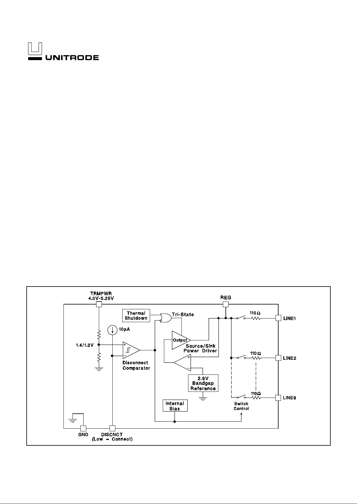
The UC5604 provides 9 lines of active termination for a SCSI (Small Computer Systems Interface) parallel bus. The SCSI standard recommends active termination at both ends of the cable segment.
The UC5604 provides a disconnect feature which, when opened or driven
high, will disconnect all terminating resistors and disable the regulator,
greatly redu cing stan dby power. The output c hannels remain high impedance even without Termpwr applied.
The UC5604 is pin-for-pin compatibl e with its predeces sor, the UC5603 - 9
line Active Terminator. The only functiona l differ ence be twee n the UC5604
and UC5603 is the absence of the negative clamps. Parametrically, the
UC5604 has a 7 % tol er ance o n im peda nce and current compared to a 3%
tolerance on the UC5603 and the sink current is reduced from 300mA to
40mA. Custom power packages are utilized to allow normal operation at
full power conditions (1.2 watts).
Internal circuit trimming is utilized, first to trim the impedance to a 7% tolerance, and the n most importantly, to trim the output current to a 7% tolerance, as close to the max SCSI spec as possible, which maximiz es noise
margin in fast SCSI operation.
Other features include thermal shutdown and current limit.
This device is offered in low thermal resistance versions of the industry
standard 16 pin narrow body SO IC, 16 pin ZIP (zig-zag in line package)
and 24 pin TSSOP.
UC5604
9-Line Low Capacitance SCSI Active Terminator
FEATURES DESCRIPTION
BLOCK DIAGRAM
Circuit Design Patented
3/97
UDG-94064

ABSOLUTE MAXIMUM RATINGS
Termpwr Vo ltage . . . . . . . . . . . . . . . . . . . . . . . . . . . . . . . . . . . . . . . . . . . . . . . . . . . +7V
Signal Line Voltage. . . . . . . . . . . . . . . . . . . . . . . . . . . . . . . . . . . . . . . . . . . . . 0V to +7V
Regulator Output Current . . . . . . . . . . . . . . . . . . . . . . . . . . . . . . . . . . . . . . . . . . . . 0.5A
Storage Temperature . . . . . . . . . . . . . . . . . . . . . . . . . . . . . . . . . . . . . −65°C to +150°C
Operating Temperature . . . . . . . . . . . . . . . . . . . . . . . . . . . . . . . . . . . −55°C to +150°C
Lead Temperature (Soldering, 10 Sec.) . . . . . . . . . . . . . . . . . . . . . . . . . . . . . . . +300°C
RECOMMENDED OPERATING CONDITIONS
Termpwr Voltage . . . . . . . . . . . . . . . . . . . . . . . . . . . . . . . . . . . . . . . . . . . 3.8V to 5.25V
Signal Line Voltage. . . . . . . . . . . . . . . . . . . . . . . . . . . . . . . . . . . . . . . . . . . . . 0V to +5V
Disconnect Input Voltage . . . . . . . . . . . . . . . . . . . . . . . . . . . . . . . . . . . . 0V to Termpwr
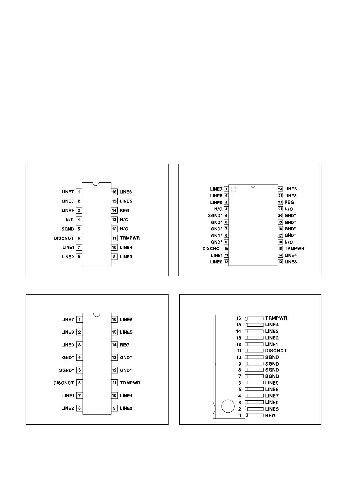
CONNECTION DIAGRAMS
DIL-16 (Top View)
N or J Package
UC5604
* DP packag e pi n 5 se rves as signal ground; pin s 4, 12, 13
serve as heatsink/ground.
* PWP package pin 5 serves as signal ground; pins 6, 7, 8, 9,
17, 18, 19, and 20 serve as heatsink/ground.
ZIP-16 (Top View)
Z Package
SOIC-16 (Top View)
DP Package
TSSOP-24 (To p View)
PWP Package
Note: Drawings are not to scale.
Unless otherwise sp ec ified all voltages are with respect to G round. Currents are positive into, negative out of the specified terminal.
Consult Packaging Section of Unitrode Integrated Circuits databook for thermal limitations and consid era ti on s of pac ka ges.
2
 Loading...