UC1965
UC2965
UC3965
SLUS300A - APRIL 1999
FEATURES
•
Accessible 2.5V Precision Reference
•
0.4% Initial Reference Accuracy
•
1% Reference Accuracy over Line,
Load, and Full Temperature Range
•
Low 1mV Offset Error Amplifier
•
Supports Closed Loop Soft Start
•
2X Inverting Amplifier / Buffer Output
•
4.1V Undervoltage Lockout
•
ICC 2mA at 5V
•
8-Pin SOIC or DIL Package
Precision Reference with Low Offset Error Amplifier
8COMP
GND
VOUT
7VFB
6VREF
5NI
1
2
3
4
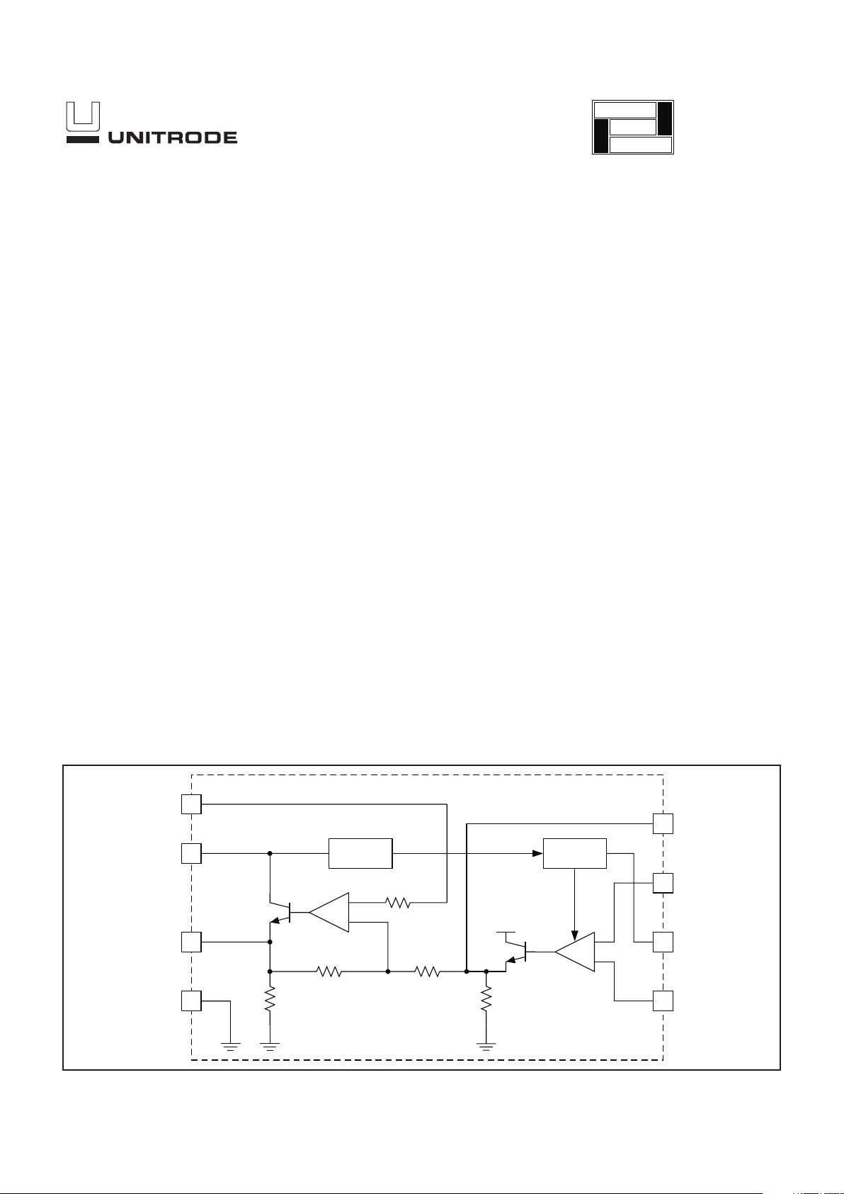
VCC
OFFSET
EA
OB
UVLO
VREF
2.5V
VCC
15k
+
–
7.5k
5k
+
–
5k
2k
BLOCK DIAGRAM
UDG-98055
DESCRIPTION
The UC3965 is suitable for applications needing greater precision and
more functionality than the TL431 type shunt regulators. The wide range
VCC input capability enables the device to be biased from the secondary
side output voltage rail, resulting in closed loop soft start.
The UC3965 includes an accessible 2.5V precision reference which offers
0.4% initial and 1% reference accuracy over line, load, and full tempera
ture range with a low offset error amplifier, a 2X inverting amplifier/buffer,
and an undervoltage lockout circuit. The IC is ideally suited for applica
tions where high precision PWM power supply regulation is required.
Typically, the error amplifier is configured to compare a fraction of the to
be regulated power supply voltage to the on-chip 2.5V reference. The 2X
amplifier/buffer output is then used to drive a PWM controller or regulator.
The UC3965 is also capable of driving an optocoupler diode for isolated
applications.
application
INFO
available

2
UC1965
UC2965
UC3965
ELECTRICAL CHARACTERISTICS
Unless otherwise specified, VCC = 5V, TA=TJ.
PARAMETER TEST CONDITIONS MIN TYP MAX UNITS
General
VCC 4.3 20 V
Operating Current VCC = 5V 1.5 2 4 mA
Undervoltage Current 200 µA
Minimum Voltage to Start 3.9 4.1 4.3 V
Hysteresis 200 300 400 mV
VREF
VREF Initial Accuracy +25°C 2.49 2.5 2.51 V
VREF Over Temperature –55°C to +125°C 2.48 2.5 2.52 V
Total Output Variation Line, Load, Temperature 2.475 2.5 2.525 V
Line Regulation VCC = 4.3V to 20V 2 10 mV
Load Regulation 0µA to 500µA 2 10 mV
Short Circuit Current VREF = 0V 2 mA
Error Amplifier
Input Bias V
CM
= 2.5V 200 400 nA
Input Offset Voltage V
CM
= 2.5V 1 2 mV
Input Offset Current V
CM
= 2.5V –100 0 100 nA
Gain Bandwidth Product V
IN
= 50mV P-P (Note 1) 6 MHz
Open Loop Gain VOUT = 1V to 3.75V 80 100 dB
VREF
VFB
COMP
NI
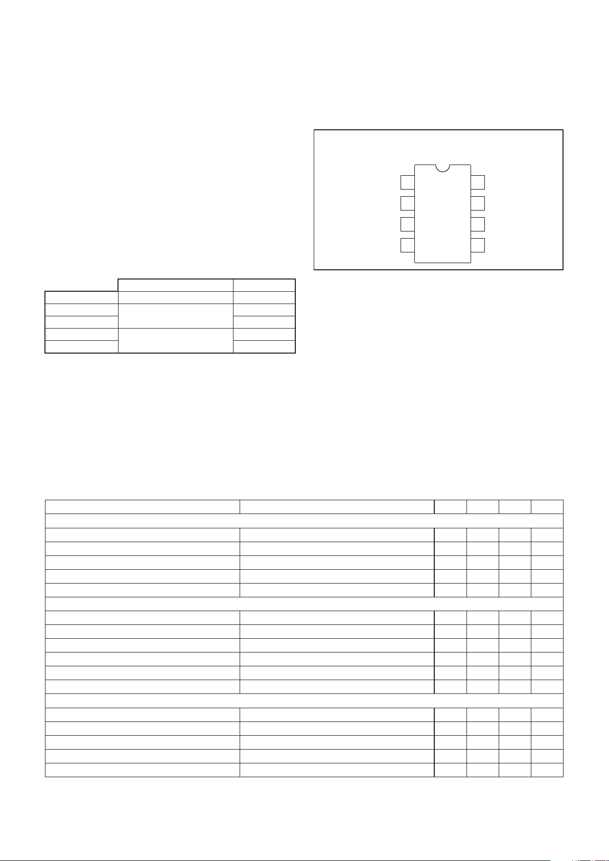
1
2
3
4
8
7
6
5
VCC
OFFSET
VOUT
GND
CONNECTION DIAGRAM
DIL-8, SOIC-8 (Top View)
J or N Package, D Package
ABSOLUTE MAXIMUM RATINGS
VCC. . . . . . . . . . . . . . . . . . . . . . . . . . . . . . . . . . . . –0.3V to 20V
VREF. . . . . . . . . . . . . . . . . . . . . . . . . . . . . . . . . . . . –0.3V to 6V
VFB, COMP, NI, VOUT. . . . . . . . . . . . . . . . . . . . . –0.3V TO 6V
Storage Temperature . . . . . . . . . . . . . . . . . . . −65°C to +150°C
Junction Temperature. . . . . . . . . . . . . . . . . . . –55°C to +150°C
Lead Temperature (Soldering, 10 sec.) . . . . . . . . . . . . . +300°C
Currents are positive into, negative out of the specified terminal.
All voltages are with respect to ground. Consult Packaging Sec
tion of Databook for thermal limitations and considerations of
packages.
TEMPERATURE RANGE PACKAGE
UC1965J –55°C to +125°C CDIP
UC2965D –40°C to +85°C SOIC
UC2965N PDIP
UC3965D 0°C to +70°C SOIC
UC3965N PDIP
ORDERING INFORMATION
 Loading...