

uA9638C
DUAL HIGH-SPEED DIFFERENTIAL LINE DRIVER
SLLS112C – OCTOBER 1980 – REVISED APRIL 1994
1
POST OFFICE BOX 655303 • DALLAS, TEXAS 75265
D
Meets or Exceeds ANSI Standard
EIA/TIA-422-B
D
Operates From a Single 5-V Power Supply
D
Drives Loads as Low as 50 Ω up
to 15 Mbps
D
TTL- and CMOS-Input Compatibility
D
Output Short-Circuit Protection
D
Interchangeable With National
Semiconductor DS9638
description
The uA9638C is a dual high-speed differential line driver designed to meet ANSI Standard EIA/TIA-422-B. The
inputs are TTL and CMOS compatible and have input clamp diodes. Schottky-diode-clamped transistors are
used to minimize propagation delay time. This device operates from a single 5-V power supply and is supplied
in an 8-pin package.
The uA9638 provides the current needed to drive low-impedance loads at high speeds. Typically used with
twisted-pair cabling and differential receiver(s), base-band data transmission can be accomplished up to and
exceeding 15 Mbps in properly designed systems. The uA9637A dual line receiver is commonly used as the
receiver. For even faster switching speeds in the same pin configuration, see the SN75ALS191.
The uA9638C is characterized for operation from 0°C to 70°C.
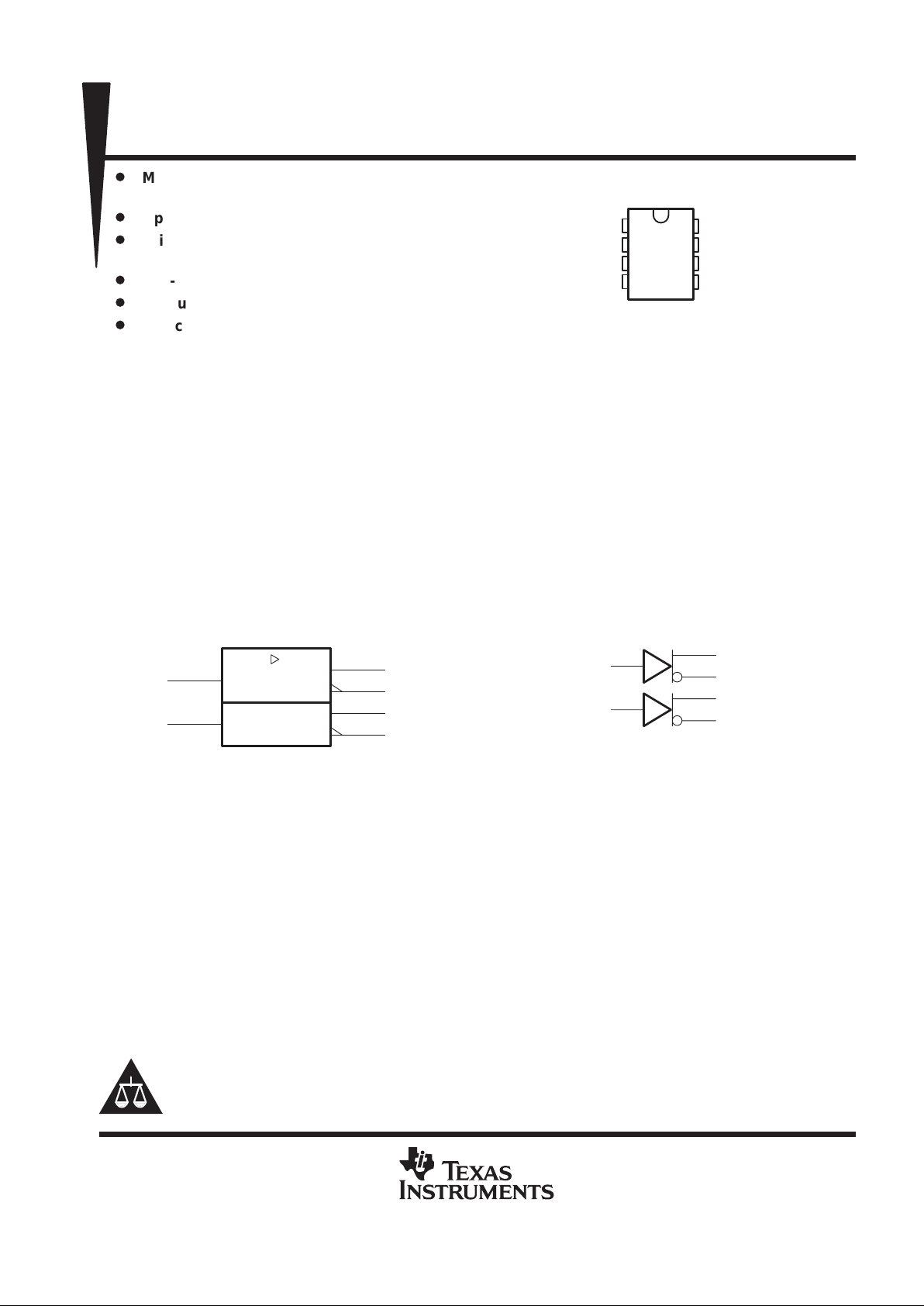
logic symbol
†
†
This symbol is in accordance with ANSI/IEEE Std 91-1984 and
IEC Publication 617-12.
2A
1A
5
6
7
8
2Z
2Y
1Z
1Y
3
2
logic diagram
2Z
2Y
1Z
1Y
3
2
2A
1A
5
6
7
8
Copyright 1994, Texas Instruments Incorporated
PRODUCTION DATA information is current as of publication date.
Products conform to specifications per the terms of Texas Instruments
standard warranty. Production processing does not necessarily include
testing of all parameters.
Please be aware that an important notice concerning availability, standard warranty, and use in critical applications of
Texas Instruments semiconductor products and disclaimers thereto appears at the end of this data sheet.
National Semiconductor is a trademark of National Semiconductor Corporation.
1
2
3
4
8
7
6
5
V
CC
1A
2A
GND
1Y
1Z
2Y
2Z
D OR P PACKAGE
(TOP VIEW)
uA9638C
DUAL HIGH-SPEED DIFFERENTIAL LINE DRIVER
SLLS112C – OCTOBER 1980 – REVISED APRIL 1994
2
POST OFFICE BOX 655303 • DALLAS, TEXAS 75265
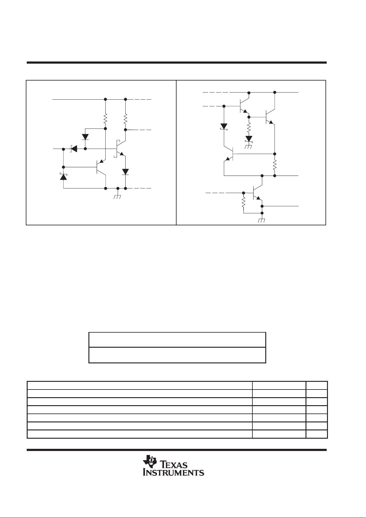
schematics of inputs and outputs
V
CC
EQUIVALENT OF EACH INPUT
TYPICAL OF ALL OUTPUTS
Input
4 kΩ NOM
V
CC
Output
GND
9.6 Ω NOM
absolute maximum ratings over operating free-air temperature range (unless otherwise noted)
†
Supply voltage range, V
CC
(see Note 1) –0.5 V to 7 V. . . . . . . . . . . . . . . . . . . . . . . . . . . . . . . . . . . . . . . . . . . . . .
Input voltage range, V
I
–0.5 V to 7 V. . . . . . . . . . . . . . . . . . . . . . . . . . . . . . . . . . . . . . . . . . . . . . . . . . . . . . . . . . . . . .
Continuous total power dissipation See Dissipation Rating Table. . . . . . . . . . . . . . . . . . . . . . . . . . . . . . . . . . . . .
Operating free-air temperature range, T
A
0°C to 70°C. . . . . . . . . . . . . . . . . . . . . . . . . . . . . . . . . . . . . . . . . . . . . .
Storage temperature range, T
stg
–65°C to 150°C. . . . . . . . . . . . . . . . . . . . . . . . . . . . . . . . . . . . . . . . . . . . . . . . . . .
Lead temperature 1,6 mm (1/16 inch) from 10 seconds 260°C. . . . . . . . . . . . . . . . . . . . . . . . . . . . . . . . . . . . . . .
†
Stresses beyond those listed under “absolute maximum ratings” may cause permanent damage to the device. These are stress ratings only, and
functional operation of the device at these or any other conditions beyond those indicated under “recommended operating conditions” is not
implied. Exposure to absolute-maximum-rated conditions for extended periods may affect device reliability.
NOTE 1: Voltage values except differential output voltages are with respect to network GND.
DISSIPATION RA TING TABLE
T
= 25°C DERATING FACTOR T
= 70°C
PACKAGE
A
POWER RATING ABOVE TA = 25°CAPOWER RATING
D 725 mW 5.8 mW/°C 464 mW
P 1000 mW 8.0 mW/°C 640 mW
recommended operating conditions
MIN NOM MAX UNIT
Supply voltage, V
CC
4.75 5 5.25 V
High-level input voltage, V
IH
2 V
Low-level input voltage, V
IL
0.8 V
High-level output current, I
OH
–50 mA
Low-level output current, I
OL
50 mA
Operating free-air temperature, T
A
0 70 °C

uA9638C
DUAL HIGH-SPEED DIFFERENTIAL LINE DRIVER
SLLS112C – OCTOBER 1980 – REVISED APRIL 1994
3
POST OFFICE BOX 655303 • DALLAS, TEXAS 75265
electrical characteristics over operating free-air temperature range (unless otherwise noted)
PARAMETER TEST CONDITIONS MIN TYP†MAX UNIT
V
IK
Input clamp voltage VCC = 4.75 V , II = –18 mA –1 –1.2 V
p
V
= 4.75 V , V
= 2 V,
IOH = –10 mA 2.5 3.5
VOHHigh-level output voltage
CC
,
VIL = 0.8 V
IH
,
IOH = –40 mA 2
V
p
V
= 4.75 V , V
= 2 V, V
= 0.8 V,
VOLLow-level output voltage
CC
,
IOL = 40 mA
IH,IL
,
0.5
V
|V
OD1
| Magnitude of differential output voltage VCC = 5.25 V , IO = 0 2V
OD2
V
|V
OD2
| Magnitude of differential output voltage 2 V
Change in magnitude of differential
∆|VOD|
Change in magnitude of differential
output voltage
‡
V
= 4.75 V to 5.25 V , R
= 100 Ω,
±0.4
V
V
OC
Common-mode output voltage
§
CC
,
See Figure 1
L
,
3 V
Change in magnitude of common-mode
∆|VOC|
Change in magnitude of common mode
output voltage
‡
±0.4
V
VO = 6 V 0.1 100
I
O
Output current with power off VCC = 0
VO = – 0.25 V –0.1 –100
µA
VO = – 0.25 V to 6 V ±100
I
I
Input current VCC = 5.25 V , VI = 5.5 V 50 µA
I
IH
High-level input current VCC = 5.25 V , VI = 2.7 V 25 µA
I
IL
Low-level input current VCC = 5.25 V , VI = 0.5 V –200 µA
I
OS
Short-circuit output current
¶
VCC = 5.25 V , VO = 0 –50 –150 mA
I
CC
Supply current (both drivers) VCC = 5.25 V , No load, All inputs at 0 V 45 65 mA
†
All typical values are at VCC = 5 V and TA = 25°C.
‡
∆| VOD | and ∆| VOC | are the changes in magnitude of VOD and VOC, respectively, that occur when the input is changed from a high level to a
low level or vice versa.
§
In Standard EIA-422-A, VOC, which is the average of the two output voltages with respect to ground, is called output offset voltage, VOS.
¶
Only one output at a time should be shorted, and duration of the short circuit should not exceed one second.
switching characteristics, VCC = 5 V, TA = 25°C
PARAMETER TEST CONDITIONS MIN TYP MAX UNIT
t
d(OD)
Differential output delay time
p
10 20 ns
t
t(OD)
Differential output transition time
C
L
= 15 pF,
R
L
=
100 Ω
,
See Figure 2
10 20 ns
t
sk(o)
Output skew See Figure 2 1 ns
uA9638C
DUAL HIGH-SPEED DIFFERENTIAL LINE DRIVER
SLLS112C – OCTOBER 1980 – REVISED APRIL 1994
4
POST OFFICE BOX 655303 • DALLAS, TEXAS 75265
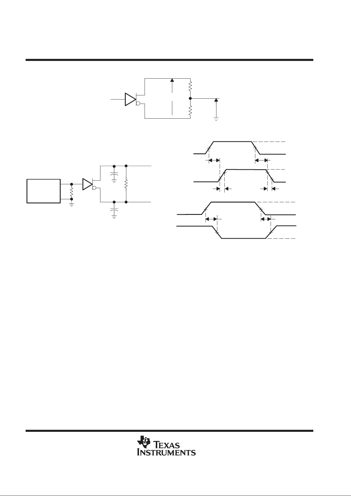
PARAMETER MEASUREMENT INFORMATION
50 Ω
V
OC
50 Ω
Input
V
OD2
Figure 1. Differential and Common-Mode Output Voltages
Differential
Output
t
d(OD)
TEST CIRCUIT
Z Output
CL = 15 pF
(see Note B)
50 Ω
VOLTAGE WAVEFORMS
Input
1.5 V
3 V
t
t(OD)
0 V
t
d(OD)
10%
10%
90%
90%
Y Output
RL = 100 Ω
C
L
1.5 V
t
t(OD)
V
OL
50%
V
OL
50%
t
sk(o)
t
sk(o)
Y Output
Z Output
V
OH
V
OH
Generator
(see Note A)
50% 50%
NOTES: A. The input pulse generator has the following characteristics: ZO = 50 Ω, PRR ≤ 500 kHz, tw = 100 ns, tr = ≤ 5 ns.
B. CL includes probe and jig capacitance.
Figure 2. Test Circuit and Voltage Waveforms

IMPORTANT NOTICE
T exas Instruments and its subsidiaries (TI) reserve the right to make changes to their products or to discontinue
any product or service without notice, and advise customers to obtain the latest version of relevant information
to verify, before placing orders, that information being relied on is current and complete. All products are sold
subject to the terms and conditions of sale supplied at the time of order acknowledgement, including those
pertaining to warranty, patent infringement, and limitation of liability.
TI warrants performance of its semiconductor products to the specifications applicable at the time of sale in
accordance with TI’s standard warranty. Testing and other quality control techniques are utilized to the extent
TI deems necessary to support this warranty. Specific testing of all parameters of each device is not necessarily
performed, except those mandated by government requirements.
CERT AIN APPLICATIONS USING SEMICONDUCTOR PRODUCTS MAY INVOLVE POTENTIAL RISKS OF
DEATH, PERSONAL INJURY, OR SEVERE PROPERTY OR ENVIRONMENTAL DAMAGE (“CRITICAL
APPLICATIONS”). TI SEMICONDUCTOR PRODUCTS ARE NOT DESIGNED, AUTHORIZED, OR
WARRANTED TO BE SUITABLE FOR USE IN LIFE-SUPPORT DEVICES OR SYSTEMS OR OTHER
CRITICAL APPLICATIONS. INCLUSION OF TI PRODUCTS IN SUCH APPLICA TIONS IS UNDERST OOD TO
BE FULLY AT THE CUSTOMER’S RISK.
In order to minimize risks associated with the customer’s applications, adequate design and operating
safeguards must be provided by the customer to minimize inherent or procedural hazards.
TI assumes no liability for applications assistance or customer product design. TI does not warrant or represent
that any license, either express or implied, is granted under any patent right, copyright, mask work right, or other
intellectual property right of TI covering or relating to any combination, machine, or process in which such
semiconductor products or services might be or are used. TI’s publication of information regarding any third
party’s products or services does not constitute TI’s approval, warranty or endorsement thereof.
Copyright 1998, Texas Instruments Incorporated
 Loading...