

uA9636AC
DUAL LINE DRIVER WITH ADJUSTABLE SLEW RATE
SLLS110B – OCTOBER 1980 – REVISED MAY 1995
D
Meets or Exceeds the Requirements of
ANSI Standards EIA/TIA-423-B and -232-E
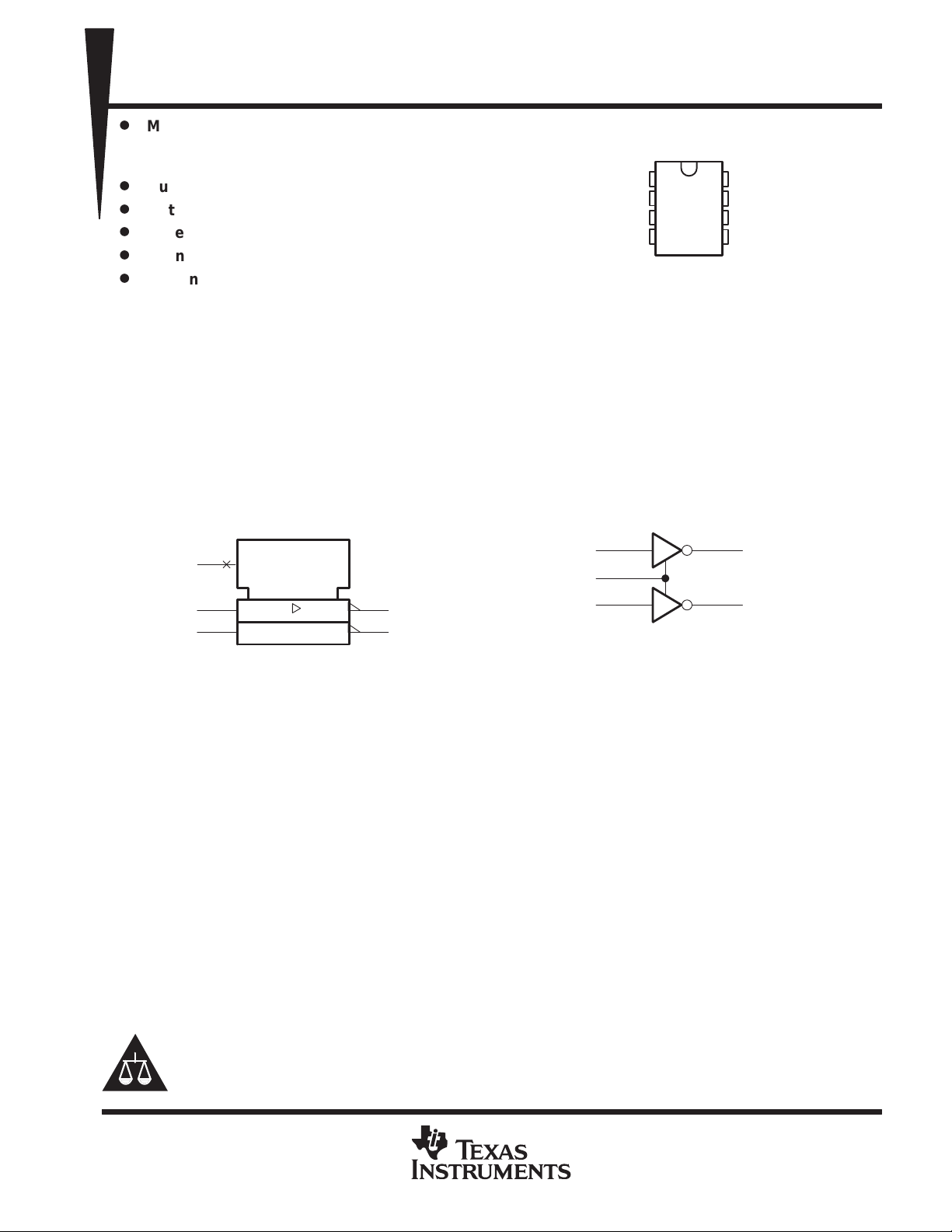
D OR P PACKAGE
(TOP VIEW)
and ITU Recommendations V.10 and V.28
D
Output Slew Rate Control
D
Output Short-Circuit-Current Limiting
D
Wide Supply Voltage Range
D
8-Pin Package
D
Designed to Be Interchangeable With
National DS9636A
W-S
1A
2A
GND
1
2
3
4
V
8
CC+
1Y
7
2Y
6
5
V
CC–
description
The uA9636AC is a dual, single-ended line driver designed to meet ANSI Standards EIA/TIA-423-B and
EIA/TIA-232-E and ITU Recommendations V.10 and V.28. The slew rates of both amplifiers are controlled by
a single external resistor, R
current limiting is provided. Inputs are compatible with TTL and CMOS and are diode protected against negative
transients. This device operates from ±12 V and is supplied in an 8-pin package.
The uA9636AC is characterized for operation from 0°C to 70°C.
W-S
1A
2A
†
1
2
3
[Slew-Rate]
logic symbol
†
This symbol is in accordance with ANSI/IEEE Std 91-1984
and IEC Publication 617-12.
, connected between the wave-shape-control (W-S) terminal and GND. Output
(WS)
logic diagram
2
1A
1
W-S
7
1Y
6
2Y
2A
3
7
1Y
6
2Y
Please be aware that an important notice concerning availability, standard warranty, and use in critical applications of
Texas Instruments semiconductor products and disclaimers thereto appears at the end of this data sheet.
PRODUCTION DATA information is current as of publication date.
Products conform to specifications per the terms of Texas Instruments
standard warranty. Production processing does not necessarily include
testing of all parameters.
POST OFFICE BOX 655303 • DALLAS, TEXAS 75265
Copyright 1995, Texas Instruments Incorporated
1
uA9636AC
PACKAGE
A
A
DUAL LINE DRIVER WITH ADJUSTABLE SLEW RATE
SLLS110B – OCTOBER 1980 – REVISED MAY 1995
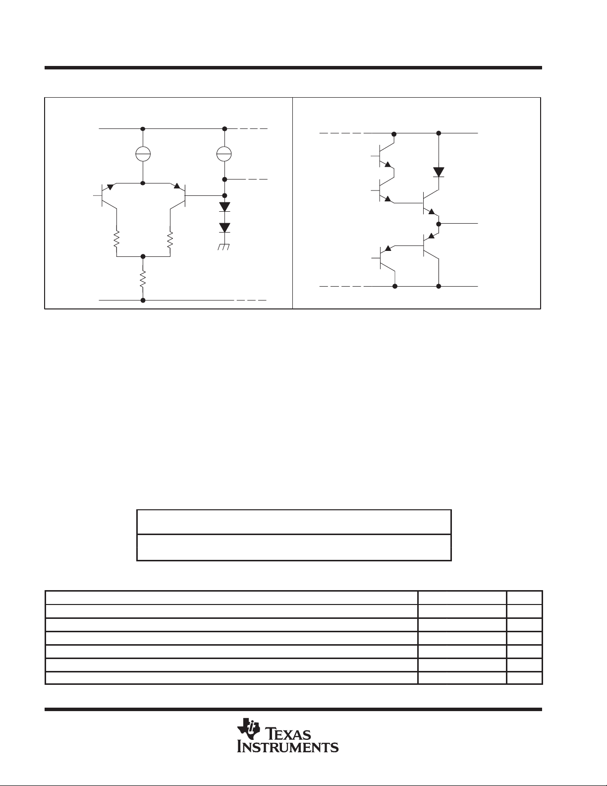
schematics of inputs and outputs
V
CC+
Input
V
CC±
EQUIVALENT OF EACH INPUT
Current
Source
Current
Source
TYPICAL OF ALL OUTPUTS
V
CC+
Output
V
CC±
absolute maximum ratings over operating free-air temperature range (unless otherwise noted)
Positive supply voltage range, V
Negative supply voltage range, V
Output voltage, V
Output current, I
±15 V. . . . . . . . . . . . . . . . . . . . . . . . . . . . . . . . . . . . . . . . . . . . . . . . . . . . . . . . . . . . . . . . . . . . . . . .
O
±150 mA. . . . . . . . . . . . . . . . . . . . . . . . . . . . . . . . . . . . . . . . . . . . . . . . . . . . . . . . . . . . . . . . . . . . . .
O
Continuous total power dissipation See Dissipation Rating Table. . . . . . . . . . . . . . . . . . . . . . . . . . . . . . . . . . . . .
Operating free-air temperature range, T
Storage temperature range, T
stg
Lead temperature 1,6 mm (1/16 inch) from case for 10 seconds 260°C. . . . . . . . . . . . . . . . . . . . . . . . . . . . . . .
†
Stresses beyond those listed under “absolute maximum ratings” may cause permanent damage to the device. These are stress ratings only, and
functional operation of the device at these or any other conditions beyond those indicated under “recommended operating conditions” is not
implied. Exposure to absolute-maximum-rated conditions for extended periods may affect device reliability.
NOTE 1: All voltage values are with respect to the network ground terminal.
(see Note 1) V
CC+
0.5 V to –15 V. . . . . . . . . . . . . . . . . . . . . . . . . . . . . . . . . . . . . . . . . . . . . . .
CC–
0°C to 70°C. . . . . . . . . . . . . . . . . . . . . . . . . . . . . . . . . . . . . . . . . . . . . .
A
–65°C to 150°C. . . . . . . . . . . . . . . . . . . . . . . . . . . . . . . . . . . . . . . . . . . . . . . . . . .
CC–
to 15 V. . . . . . . . . . . . . . . . . . . . . . . . . . . . . . . . . . . . . .
†
T
POWER RATING ABOVE TA = 25°C
D 725 mW 5.8 mW/°C 464 mW
P 1000 mW 8.0 mW/°C 640 mW
recommended operating conditions
Positive supply voltage, V
Negative supply voltage, V
High-level input voltage, V
Low-level input voltage, V
Wave-shaping resistor , R
Operating free-air temperature, T
2
CC+
CC–
IH
IL
(WS)
A
POST OFFICE BOX 655303 • DALLAS, TEXAS 75265
DISSIPATION RATING TABLE
≤ 25°C DERATING FACTOR T
POWER RATING
= 70°C
MIN NOM MAX UNIT
10.8 12 13.2 V
–10.8 –12 –13.2 V
2 V
0.8 V
10 1000 kΩ
0 70 °C
IIHHigh-level input current
A
I
Short-ci
t
§
mA
I
Positive supply current
CC
,
I
,
1318mA
I
Negative supply current
CC
I
13–18
mA
t
Transition time, lo
high-level output
R
450 kΩ
C
30 pF
s
t
Transition time, high- to low-level output
R
450 kΩ
C
pF
s
uA9636AC
DUAL LINE DRIVER WITH ADJUSTABLE SLEW RATE
SLLS110B – OCTOBER 1980 – REVISED MAY 1995
electrical characteristics over recommended ranges of free-air temperature, supply voltage, and
wave-shaping resistance (unless otherwise noted)
PARAMETER TEST CONDITIONS MIN TYP†MAX UNIT
V
IK
V
OH
V
OL
I
IL
I
O
OS
r
O
CC+
CC–
†
All typical values are at VCC = ±12 V, TA = 25°C.
‡
The algebraic convention, in which the less-positive (more-negative) limit is designated as minimum, is used in this data sheet for logic voltage
levels, e.g., when –5 V is the maximum, the minimum is a more-negative voltage.
§
Not more than one output should be shorted to ground at a time.
Input clamp voltage II = –15 mA –1.1 –1.5 V
RL = ∞ 5 5.6 6
High-level output voltage VI = 0.8 V
Low-level output voltage VI = 2 V
p
Low-level input current VI = 0.4 V –20 –80 µA
Output current (power off) V
p
rcut output curren
Output resistance RL = 450 Ω 25 50 Ω
pp
pp
VI = 2.4 V 10
VI = 5.5 V 100
= 0, VO = ± 6 V ±100 µA
CC±
VI = 2 V 15 25 150
VI = 0 –15 –40 –150
V
= ±12 V , V
R
= 100 kΩ,
(WS)
VCC = ±12 V , VI = 0,
R
= 100 kΩ,
(WS)
RL = 3 kΩ to GND 5 5.6 6
RL = 450 Ω to GND 4 5.4 6
RL = ∞ –6‡–5.7 –5
RL = 3 kΩ to GND –6‡–5.6 –5
RL = 450 Ω to GND –6‡–5.4 –4
= 0,
Output open
Output open
–
V
V
µ
switching characteristics, V
PARAMETER TEST CONDITIONS MIN TYP MAX UNIT
TLH
THL
w- to
= ±12 V, TA = 25°C (see Figure 1)
±
CC
p
p
=
L
=
L
,
,
=
L
= 30
L
p
p
R
= 10 kΩ 0.8 1.1 1.4
(WS)
R
= 100 kΩ 8 11 14
(WS)
R
= 500 kΩ 40 55 70
(WS)
R
= 1 MΩ 80 110 140
(WS)
R
= 10 kΩ 0.8 1.1 1.4
(WS)
R
= 100 kΩ 8 11 14
(WS)
R
= 500 kΩ 40 55 70
(WS)
R
= 1 MΩ 80 110 140
(WS)
µ
µ
POST OFFICE BOX 655303 • DALLAS, TEXAS 75265
3

uA9636AC
DUAL LINE DRIVER WITH ADJUSTABLE SLEW RATE
SLLS110B – OCTOBER 1980 – REVISED MAY 1995
PARAMETER MEASUREMENT INFORMATION
V
CC+
(see Note B)
Input
50 Ω
R
(WS)
R
L
Output
CL = 30 pF
(see Note A)
Input
90%
90%
3 V
0 V
V
OH
V
CC±
TEST CIRCUIT
NOTES: A. CL includes probe and jig capacitance.
B. The input pulse is supplied by a generator having the following characteristics: tr ≤ 10 ns, tf ≤ 10 ns, ZO = 50 Ω, PRR ≤ 1 kHz,
duty cycle = 50%.
Figure 1. Test Circuit and Voltage Waveforms
TYPICAL CHARACTERISTICS
OUTPUT VOLTAGE
vs
INPUT VOLTAGE
12
V
= ±12 V
CC±
10
R
= 100 kΩ
(WS)
RL = 450 Ω
8
6
4
2
0
–2
O
V
VO – Output Voltage – V
–4
–6
TA = 70°C
TA = 25°C
TA = 0°C
Output
t
THL
250
V
200
150
µ
100
50
–50
I
II – Input Current –
I
–100
–150
–200
CC±
R
(WS)
0
10%
VOLTAGE WAVEFORMS
INPUT CURRENT
vs
INPUT VOLTAGE
= ±12 V
= 100 kΩ
TA = 25°C
TA = 70°C
TA = 0°C
TA = 25°C
TA = 70°C
10%
TA = 0°C
t
TLH
V
OL
–8
0 0.4 0.8 1.2 1.6 2
VI–Input Voltage–V
Figure 2
4
POST OFFICE BOX 655303 • DALLAS, TEXAS 75265
–250
–2
VI–Input Voltage–V
Figure 3
76543210–1
8

uA9636AC
DUAL LINE DRIVER WITH ADJUSTABLE SLEW RATE
SLLS110B – OCTOBER 1980 – REVISED MAY 1995
TYPICAL CHARACTERISTICS
OUTPUT CURRENT
vs
OUTPUT VOLTAGE
(POWER ON)
50
V
= ±12 V
40
30
Am– Output Current – I
20
10
–10
–20
O
–30
–40
–50
CC±
R
= 100 kΩ
(WS)
TA = 25°C
VI = 2 V
0
VI = 0
–10
–8 –6 –4 –2 0 2 4 6 8
VO – Output Voltage – V
10
Aµ– Output Current – I
O
100
80
60
40
20
–20
–40
–60
–80
–100
0
–10
V
CC
VI = 0
TA = 25°C
Figure 4
OUTPUT CURRENT
OUTPUT VOLTAGE
(POWER OFF)
= 0
"
VO – Output Voltage – V
Figure 5
vs
86420–2–4–6–8
10
TLH
t
, – Transition Time – µs
TLH
t
1000
700
400
200
100
70
40
20
10
7
4
2
1
0.01
TRANSITION TIME
vs
WAVE-SHAPING RESISTANCE
TA = 0°C
TA = 70°C
0.10.04 0.4 1 4
R
– Wave-Shaping Resistance – MΩ
(WS)
Figure 6
10
POST OFFICE BOX 655303 • DALLAS, TEXAS 75265
5

uA9636AC
DUAL LINE DRIVER WITH ADJUSTABLE SLEW RATE
SLLS110B – OCTOBER 1980 – REVISED MAY 1995
APPLICATION INFORMATION
R
(WS)
12 V
uA9636A uA9637A
–12 V
Twisted Pair
or
Flat Cable
5 V
Figure 7. EIA/TIA-423-B System Application
6
POST OFFICE BOX 655303 • DALLAS, TEXAS 75265

IMPORTANT NOTICE
T exas Instruments and its subsidiaries (TI) reserve the right to make changes to their products or to discontinue
any product or service without notice, and advise customers to obtain the latest version of relevant information
to verify, before placing orders, that information being relied on is current and complete. All products are sold
subject to the terms and conditions of sale supplied at the time of order acknowledgement, including those
pertaining to warranty, patent infringement, and limitation of liability.
TI warrants performance of its semiconductor products to the specifications applicable at the time of sale in
accordance with TI’s standard warranty. Testing and other quality control techniques are utilized to the extent
TI deems necessary to support this warranty . Specific testing of all parameters of each device is not necessarily
performed, except those mandated by government requirements.
CERT AIN APPLICATIONS USING SEMICONDUCTOR PRODUCTS MAY INVOLVE POTENTIAL RISKS OF
DEATH, PERSONAL INJURY, OR SEVERE PROPERTY OR ENVIRONMENTAL DAMAGE (“CRITICAL
APPLICATIONS”). TI SEMICONDUCTOR PRODUCTS ARE NOT DESIGNED, AUTHORIZED, OR
WARRANTED TO BE SUITABLE FOR USE IN LIFE-SUPPORT DEVICES OR SYSTEMS OR OTHER
CRITICAL APPLICA TIONS. INCLUSION OF TI PRODUCTS IN SUCH APPLICATIONS IS UNDERST OOD TO
BE FULLY AT THE CUSTOMER’S RISK.
In order to minimize risks associated with the customer’s applications, adequate design and operating
safeguards must be provided by the customer to minimize inherent or procedural hazards.
TI assumes no liability for applications assistance or customer product design. TI does not warrant or represent
that any license, either express or implied, is granted under any patent right, copyright, mask work right, or other
intellectual property right of TI covering or relating to any combination, machine, or process in which such
semiconductor products or services might be or are used. TI’s publication of information regarding any third
party’s products or services does not constitute TI’s approval, warranty or endorsement thereof.
Copyright 1998, Texas Instruments Incorporated
 Loading...