


TVP5150AM1
www.ti.com
SLES209D–NOVEMBER 2007–REVISED SEPTEMBER 2010
Ultralow-Power NTSC/PAL/SECAM Video Decoder
Check for Samples: TVP5150AM1
1 Introduction
1.1 Features
1
• Accepts NTSC (J, M, 4.43), PAL (B, D, G, H, I, • Standard Programmable Video Output Formats
M, N, Nc), and SECAM (B, D, G, K, K1, L) Video
• Supports ITU-R BT.601 Standard Sampling Syncs
• High-Speed 9-Bit Analog-to-Digital Converter – 8-Bit 4:2:2 With Discrete Syncs
(ADC)
• Two Composite Inputs or One S-Video Input
• Fully Differential CMOS Analog Preprocessing Formats
Channels With Clamping and Automatic Gain
Control (AGC) for Best Signal-to-Noise (S/N)
Performance
• Ultralow Power Consumption
• 48-Terminal PBGA Package (ZQC) or
32-Terminal TQFP Package (PBS)
• Power-Down Mode: <1 mW
• Brightness, Contrast, Saturation, Hue, and
Sharpness Control Through I2C
• Complementary 4-Line (3-H Delay) Adaptive
Comb Filters for Both Cross-Luminance and
Cross-Chrominance Noise Reduction
• Patented Architecture for Locking to Weak,
Noisy, or Unstable Signals
• Single 14.31818-MHz Crystal for All Standards
• Internal Phase-Locked Loop (PLL) for Data Signals
Line-Locked Clock and Sampling
• Subcarrier Genlock Output for Synchronizing
Color Subcarrier of External Encoder
• 3.3-V Digital I/O Supply Voltage Range
– ITU-R BT.656, 8-Bit 4:2:2 With Embedded
• Macrovision™ Copy Protection Detection
• Advanced Programmable Video Output
– 2× Oversampled Raw Vertical Blanking
Interval (VBI) Data During Active Video
– Sliced VBI Data During Horizontal Blanking
or Active Video
• VBI Modes Supported
– Teletext (NABTS, WST)
– Closed-Caption Decode With FIFO and
Extended Data Services (XDS)
– Wide Screen Signaling, Video Program
System, CGMS-A, Vertical Interval Time
Code
– Gemstar 1x/2x Electronic Program Guide
Compatible Mode
– Custom Configuration Mode That Allows
User to Program Slice Engine for Unique VBI
• Power-On Reset
• Industrial Temperature Range (TVP5150AM1I):
–40°C to 85°C
• Qualified for Automotive Applications
(AEC-Q100 Rev G – TVP5150AM1IPBSQ1,
TVP5150AM1IPBSRQ)
1.2 Description
The TVP5150AM1 device is an ultralow-power NTSC/PAL/SECAM video decoder. Available in a
space-saving 48-terminal PBGA package or a 32-terminal TQFP package, the TVP5150AM1 decoder
converts NTSC, PAL, and SECAM video signals to 8-bit ITU-R BT.656 format. Discrete syncs are also
available. The optimized architecture of the TVP5150AM1 decoder allows for ultralow power consumption.
The decoder consumes 115-mW power under typical operating conditions and consumes less than 1 mW
in power-down mode, considerably increasing battery life in portable applications. The decoder uses just
one crystal for all supported standards. The TVP5150AM1 decoder can be programmed using an I2C
serial interface.
1
Please be aware that an important notice concerning availability, standard warranty, and use in critical applications of Texas
Instruments semiconductor products and disclaimers thereto appears at the end of this data sheet.
PRODUCTION DATA information is current as of publication date.
Products conform to specifications per the terms of the Texas
Instruments standard warranty. Production processing does not
necessarily include testingof all parameters.
Copyright © 2007–2010, Texas Instruments Incorporated

TVP5150AM1
SLES209D–NOVEMBER 2007–REVISED SEPTEMBER 2010
The TVP5150AM1 decoder converts baseband analog video into digital YCbCr 4:2:2 component video.
Composite and S-video inputs are supported. The TVP5150AM1 decoder includes one 9-bit
analog-to-digital converter (ADC) with 2× sampling. Sampling is ITU-R BT.601 (27.0 MHz, generated from
the 14.31818-MHz crystal or oscillator input) and is line locked. The output formats can be 8-bit 4:2:2 or
8-bit ITU-R BT.656 with embedded synchronization.
The TVP5150AM1 decoder utilizes Texas Instruments patented technology for locking to weak, noisy, or
unstable signals. A Genlock/real-time control (RTC) output is generated for synchronizing downstream
video encoders.
Complementary four-line adaptive comb filtering is available for both the luminance and chrominance data
paths to reduce both cross-luminance and cross-chrominance artifacts; a chrominance trap filter is also
available.
Video characteristics including hue, brightness, saturation, and sharpness may be programmed using the
industry standard I2C serial interface. The TVP5150AM1 decoder generates synchronization, blanking,
lock, and clock signals in addition to digital video outputs. The TVP5150AM1 decoder includes methods
for advanced vertical blanking interval (VBI) data retrieval. The VBI data processor slices, parses, and
performs error checking on teletext, closed caption, and other data in several formats.
The TVP5150AM1 decoder detects copy-protected input signals according to the Macrovision™ standard
and detects Type 1, 2, 3, and colorstripe processes.
The main blocks of the TVP5150AM1 decoder include:
• Robust sync detector
• ADC with analog processor
• Y/C separation using four-line adaptive comb filter
• Chrominance processor
• Luminance processor
• Video clock/timing processor and power-down control
• Output formatter
• I2C interface
• VBI data processor
• Macrovision detection for composite and S-video
www.ti.com
2 Introduction Copyright © 2007–2010, Texas Instruments Incorporated
Submit Documentation Feedback
Product Folder Link(s): TVP5150AM1

TVP5150AM1
www.ti.com
1.3 Applications
The following is a partial list of suggested applications:
• Digital televisions
• PDAs
• Notebook PCs
• Cell phones
• Video recorder/players
• Internet appliances/web pads
• Handheld games
• Surveillance
• Portable navigation
• Portable video projectors
1.4 Related Products
• TVP5151
• TVP5154A
• TVP5146M2
• TVP5147M1
• TVP5158
SLES209D–NOVEMBER 2007–REVISED SEPTEMBER 2010
1.5 Trademarks
TI and MicroStar Junior are trademarks of Texas Instruments.
Macrovision is a trademark of Macrovision Corporation.
Gemstar is a trademark of Gemstar-TV Guide International.
Other trademarks are the property of their respective owners.
1.6 Document Conventions
Throughout this data manual, several conventions are used to convey information. These conventions are:
• To identify a binary number or field, a lower case b follows the numbers. For example, 000b is a 3-bit
binary field.
• To identify a hexadecimal number or field, a lower case h follows the numbers. For example, 8AFh is a
12-bit hexadecimal field.
• All other numbers that appear in this document that do not have either a b or h following the number
are assumed to be decimal format.
• If the signal or terminal name has a bar above the name (for example, RESETB), this indicates the
logical NOT function. When asserted, this signal is a logic low, 0, or 0b.
• RSVD indicates that the referenced item is reserved.
Copyright © 2007–2010, Texas Instruments Incorporated Introduction 3
Submit Documentation Feedback
Product Folder Link(s): TVP5150AM1
TVP5150AM1
SLES209D–NOVEMBER 2007–REVISED SEPTEMBER 2010
1.7 Ordering Information
T
A
0°C to 70°C
-40°C to 85°C
(1) For the most current package and ordering information, see the Package Option Addendum at the end
of this document, or see the TI web site at www.ti.com.
(2) Package drawings, thermal data, and symbolization are available at www.ti.com/packaging.
(3) AEC-Q100 Rev G Certified
PACKAGED DEVICES
(1) (2)
PACKAGE OPTION
TVP5150AM1PBS Tray
TVP5150AM1PBSR Tape and reel
TVP5150AM1ZQC Tray
TVP5150AM1ZQCR Tape and reel
TVP5150AM1IPBS Tray
TVP5150AM1IPBSR Tape and reel
TVP5150AM1IPBSQ1
TVP5150AM1IPBSRQ1
(3)
(3)
Tape and reel
TVP5150AM1IZQC Tray
TVP5150AM1IZQCR Tape and reel
www.ti.com
Tray
4 Introduction Copyright © 2007–2010, Texas Instruments Incorporated
Submit Documentation Feedback
Product Folder Link(s): TVP5150AM1

TVP5150AM1
www.ti.com
1 Introduction .............................................. 1
1.1 Features .............................................. 1
1.2 Description ........................................... 1 3.15 I2C Host Interface ................................... 19
1.3 Applications .......................................... 3 3.16 Clock Circuits ....................................... 22
1.4 Related Products ..................................... 3
1.5 Trademarks .......................................... 3
1.6 Document Conventions .............................. 3
1.7 Ordering Information ................................. 4
2 Device Details ............................................ 6
2.1 Functional Block Diagram ............................ 6
2.2 Terminal Diagrams ................................... 7
2.3 Terminal Functions ................................... 8
4 Electrical Specifications ............................. 74
3 Functional Description ............................... 10
3.1 Analog Front End ................................... 10
3.2 Composite Processing Block Diagram ............. 10
3.3 Adaptive Comb Filtering ............................ 11
3.4 Color Low-Pass Filter ............................... 12
3.5 Luminance Processing ............................. 13
3.6 Chrominance Processing ........................... 13
3.7 Timing Processor ................................... 13
3.8 VBI Data Processor (VDP) ......................... 13
3.9 VBI FIFO and Ancillary Data in Video Stream ..... 14
3.10 Raw Video Data Output ............................ 15
3.11 Output Formatter ................................... 15
3.12 Synchronization Signals ............................ 15
5 Example Register Settings .......................... 78
6 Application Information .............................. 80
7 Revision History ....................................... 81
SLES209D–NOVEMBER 2007–REVISED SEPTEMBER 2010
3.13 Active Video (AVID) Cropping ...................... 17
3.14 Embedded Syncs ................................... 18
3.17 Genlock Control (GLCO) and RTC ................. 23
3.18 Reset and Power Down ............................ 24
3.19 Reset Sequence .................................... 26
3.20 Internal Control Registers .......................... 27
3.21 Register Definitions ................................. 30
4.1 Absolute Maximum Ratings ........................ 74
4.2 Recommended Operating Conditions .............. 74
4.3 Reference Clock Specifications .................... 74
4.4 Electrical Characteristics ........................... 75
4.5 DC Electrical Characteristics ....................... 75
4.6 Analog Electrical Characteristics ................... 75
4.7 Clocks, Video Data, Sync Timing ................... 76
2
4.8 I
C Host Port Timing ................................ 77
4.9 Thermal Specifications ............................. 77
5.1 Example 1 .......................................... 78
5.2 Example 2 .......................................... 79
6.1 Application Example ................................ 80
Copyright © 2007–2010, Texas Instruments Incorporated Contents 5
Submit Documentation Feedback
Product Folder Link(s): TVP5150AM1
M
U
X
AIP1A
AIP1B
PGA
A/D
Output
Formatter
YOUT[7:0]
YCbCr 8-Bit
4:2:2
VBI Data
Processor (VDP)
Embedded Processor
XTAL1/OSC
XTAL2
PCLK/SCLK
Horizontal and
Color PLLs
FID/GLCO
VSYNC/PALI
INTREQ/GPCL/VBLK
HSYNC
Timing Processor
SCL
SDA
Y/C Separation
Chrominance
Processing
Luminance
Processing
Macrovision
Detection
Host
Interface
AVID
PDN
TVP5150AM1
SLES209D–NOVEMBER 2007–REVISED SEPTEMBER 2010
2 Device Details
2.1 Functional Block Diagram
www.ti.com
Figure 2-1. Functional Block Diagram
6 Device Details Copyright © 2007–2010, Texas Instruments Incorporated
Submit Documentation Feedback
Product Folder Link(s): TVP5150AM1
A
B
C
D
E
F
G
1
2 3 4 5 6
7
PBGA (ZQC) PACKAGE
(BOTTOMVIEW)
TQFP (PBS) PACKAGE
(TOP VIEW)
31 30 29 28 27
24
23
22
21
20
19
18
17
PCLK/SCLK
IO_DVDD
YOUT7/I2CSEL
YOUT6
YOUT5
YOUT4
YOUT3
YOUT2
CH_A
VDD
CH_AGND
REFM
REFP
PDN
INTREQ/GPCL/VBLK
AVID
HSYNC
32 26 25
VSYNC/PALI
FID/GLCO
SDA
SCL
DVDD
DGND
YOUT0
YOUT1
AIP1A
AIP1B
PLL_AGND
PLL_AVDD
XTAL1/OSC
XTAL2
AGND
RESETB
1
2
3
4
5
6
7
8
10 11 12 13 149 15 16
TVP5150AM1
www.ti.com
2.2 Terminal Diagrams
The TVP5150AM1 video decoder is packaged in a 48-terminal PBGA package or a 32-terminal TQFP
package. Figure 2-2 shows the terminal diagrams for both packages. Table 2-1 gives a description of the
terminals.
SLES209D–NOVEMBER 2007–REVISED SEPTEMBER 2010
Figure 2-2. Terminal Diagrams
Copyright © 2007–2010, Texas Instruments Incorporated Device Details 7
Submit Documentation Feedback
Product Folder Link(s): TVP5150AM1
TVP5150AM1
SLES209D–NOVEMBER 2007–REVISED SEPTEMBER 2010
www.ti.com
2.3 Terminal Functions
Table 2-1. Terminal Functions
TERMINAL
NAME
Analog Section
AGND E1 7 G Substrate. Connect to analog ground.
AIP1A A1 1 I range is 0-0.75 VPP, and may require an attenuator to reduce the input amplitude to the
AIP1B B1 2 I range is 0-0.75 VPP, and may require an attenuator to reduce the input amplitude to the
CH_AGND A3 31 G Analog ground
CH_AVDD A2 32 P Analog supply. Connect to 1.8-V analog supply.
NC – – No connect
PLL_AGND C2 3 G PLL ground. Connect to analog ground.
PLL_AVDD C1 4 P PLL supply. Connect to 1.8-V analog supply.
REFM A4 30 O
REFP B4 29 O
XTAL1/OSC D2 5 I External clock reference input.
XTAL2 D1 6 O
Digital Section
AVID A6 26 O video AVID output. AVID toggling during vertical blanking intervals is controlled by bit 2 of
DGND E6 19 G Digital ground
DVDD E7 20 P Digital supply. Connect to 1.8-V digital supply.
FID/GLCO C6 23 O GLCO: This serial output carries color PLL information. A slave device can decode the
HSYNC A7 25 O Horizontal synchronization signal
NO. I/O DESCRIPTION
ZQC PBS
Analog input. Connect to the video analog input via 0.1-µF capacitor. The maximum input
desired level. If not used, connect to AGND via a 0.1-µF capacitor (see Figure 6-1).
Analog input. Connect to the video analog input via 0.1-µF capacitor. The maximum input
desired level. If not used, connect to AGND via a 0.1-µF capacitor (see Figure 6-1).
B2, B3,
B6, C4,
C5,
D3–D6,
E2–E5,
F2, F5, F6
A/D reference negative output. Connect to analog ground through a 1-µF capacitor. Also, it
is recommended to connect directly to REFP through a 1-µF capacitor (see Figure 6-1).
A/D reference positive output. Connect to analog ground through a 1-µF capacitor (see
Figure 6-1).
External clock reference output. Not connected if XTAL1 is driven by an external
single-ended oscillator.
Active video indicator output. This signal is high during the horizontal active time of the
the active video cropping start pixel LSB register at address 12h (see Section 3.21.17).
FID: Odd/even field indicator or vertical lock indicator. For the odd/even indicator, a 1
indicates the odd field.
information to allow chrominance frequency control from the TVP5150AM1 decoder. Data is
transmitted at the SCLK rate in Genlock mode. In RTC mode, SCLK/4 is used.
INTREQ: Interrupt request output
INTREQ/GPCL/
VBLK
IO_DVDD G2 10 P Digital output supply. Connect to 3.3-V digital supply.
PCLK/SCLK G1 9 O System clock at either 1× or 2× the frequency of the pixel clock.
PDN A5 28 I
RESETB F1 8 I
8 Device Details Copyright © 2007–2010, Texas Instruments Incorporated
B5 27 O
GPCL/VBLK: General-purpose control logic. This terminal has two functions:
• GPCL: General-purpose output. In this mode the state of GPCL is directly programmed
via I2C.
• VBLK: Vertical blank output. In this mode the GPCL terminal indicates the vertical
blanking interval of the output video. The beginning and end times of this signal are
programmable via I2C.
Power-down terminal (active low). Puts the decoder in standby mode. Preserves the value
of the registers.
Active-low reset. RESETB can be used only when PDN = 1. When RESETB is pulled low, it
resets all the registers and restarts the internal microprocessor.
Submit Documentation Feedback
Product Folder Link(s): TVP5150AM1

TVP5150AM1
www.ti.com
SLES209D–NOVEMBER 2007–REVISED SEPTEMBER 2010
Table 2-1. Terminal Functions (continued)
TERMINAL
NAME
SCL D7 21 I/O I2C serial clock (open drain)
SDA C7 22 I/O I2C serial data (open drain)
VSYNC/PALI B7 24 O
YOUT[6:0] G5 15 O ITU-R BT.656 output/YCbCr 4:2:2 output with discrete syncs
YOUT7/I2CSEL F3 11 I/O
NO. I/O DESCRIPTION
ZQC PBS
VSYNC: Vertical synchronization signal
PALI: PAL line indicator or horizontal lock indicator. For the PAL line indicator:
1 = Noninverted line
0 = Inverted line
G3 12
F4 13
G4 14
G6 16
G7 17
F7 18
I2CSEL: Determines address for I2C (sampled during reset). A pullup or pulldown resistor is
needed (>1 kΩ) to program the terminal to the desired address.
1 = Address is BAh
0 = Address is B8h
YOUT7: Most significant bit (MSB) of ITU-R BT.656 output/YCbCr 4:2:2 output
Copyright © 2007–2010, Texas Instruments Incorporated Device Details 9
Submit Documentation Feedback
Product Folder Link(s): TVP5150AM1

TVP5150AM1
SLES209D–NOVEMBER 2007–REVISED SEPTEMBER 2010
3 Functional Description
3.1 Analog Front End
The TVP5150AM1 decoder has an analog input channel that accepts two video inputs that are
ac-coupled. The decoder supports a maximum input voltage range of 0.75 V; therefore, an attenuation of
one-half is needed for most input signals with a peak-to-peak variation of 1.5 V. The nominal parallel
termination before the input to the device is recommended to be 75 Ω. See the application diagram in
Figure 6-1 for the recommended configuration. The two analog input ports can be connected as either of
the following:
• Two selectable composite video inputs
• One S-video input
An internal clamping circuit restores the sync-tip of the ac-coupled video signal to a fixed dc level.
The programmable gain amplifier (PGA) and the automatic gain control (AGC) algorithm work together to
make sure that the input signal is amplified sufficiently to ensure the proper input range for the ADC.
The ADC has nine bits of resolution and runs at a nominal speed of 27 MHz. The clock input for the ADC
comes from the horizontal PLL.
3.2 Composite Processing Block Diagram
The composite processing block processes NTSC/PAL/SECAM signals into the YCbCr color space.
Figure 3-1 shows the basic architecture of this processing block.
www.ti.com
Figure 3-1 shows the luminance/chrominance (Y/C) separation process in the TVP5150AM1 decoder. The
composite video is multiplied by subcarrier signals in the quadrature modulator to generate the color
difference signals Cb and Cr. Cb and Cr are then low pass (LP) filtered to achieve the desired bandwidth
and to reduce crosstalk.
An adaptive four-line comb filter separates CbCr from Y. Chrominance is remodulated through another
quadrature modulator and subtracted from the line-delayed composite video to generate luminance.
Brightness, hue, saturation, and sharpness (using the peaking filter) are programmable via I2C.
The Y/C separation is bypassed for S-video input. For S-video, the remodulation path is disabled.
10 Functional Description Copyright © 2007–2010, Texas Instruments Incorporated
Submit Documentation Feedback
Product Folder Link(s): TVP5150AM1

Line
Delay
-
Peaking
Quadrature
Modulation
Quadrature
Modulation
Notch
Filter
Color
LPF ↓ 2
4-Line
Adaptive
Comb
Filter
Burst
Accumulator
(Cr)
Notch
Filter
LP
Filter
LP
Filter
Delay
Brightness
Saturation
Adjust
Delay
Cr
Y
Cb
Cb Cr
Y
Burst
Accumulator
(Cb)
Delay
Color
LPF ↓ 2
Composite
+Delay
X
Gain Factor
Bandpass
Peak
Detector
Composite
SECAM Color
Demodulation
Composite
Cr
Cb
SECAM Luminance
TVP5150AM1
www.ti.com
SLES209D–NOVEMBER 2007–REVISED SEPTEMBER 2010
Figure 3-1. Composite Processing Block Diagram (Comb/Trap Filter Bypassed for SECAM)
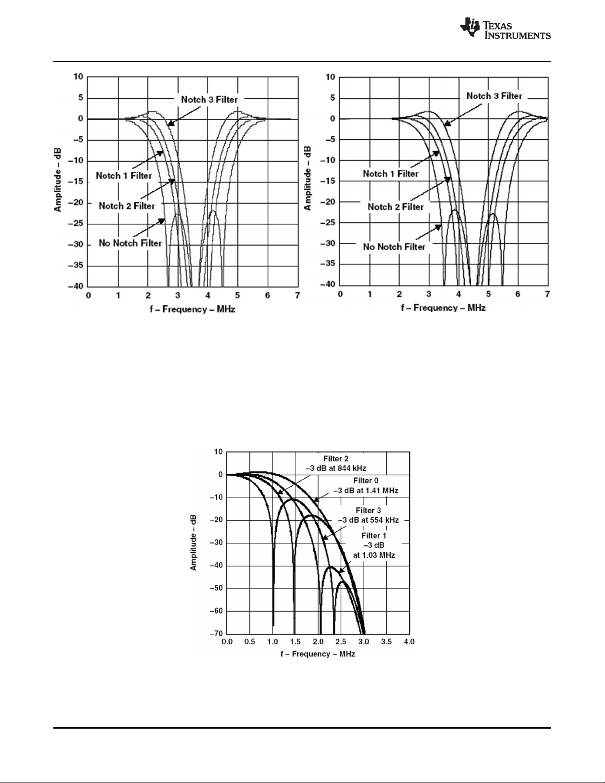
3.3 Adaptive Comb Filtering
The four-line comb filter can be selectively bypassed in the luminance or chrominance path. If the comb
filter is bypassed in the luminance path, then chrominance trap filters are used which are shown in
Figure 3-2 and Figure 3-3. TI's patented adaptive four-line comb filter algorithm reduces artifacts such as
hanging dots at color boundaries and detects and properly handles false colors in high-frequency
luminance images such as a multiburst pattern or circle pattern.
Copyright © 2007–2010, Texas Instruments Incorporated Functional Description 11
Submit Documentation Feedback
Product Folder Link(s): TVP5150AM1
TVP5150AM1
SLES209D–NOVEMBER 2007–REVISED SEPTEMBER 2010
Figure 3-2. Chrominance Trap Filter Frequency Figure 3-3. Chrominance Trap Filter Frequency
Response, NTSC ITU-R BT.601 Sampling Response, PAL ITU-R BT.601 Sampling
www.ti.com
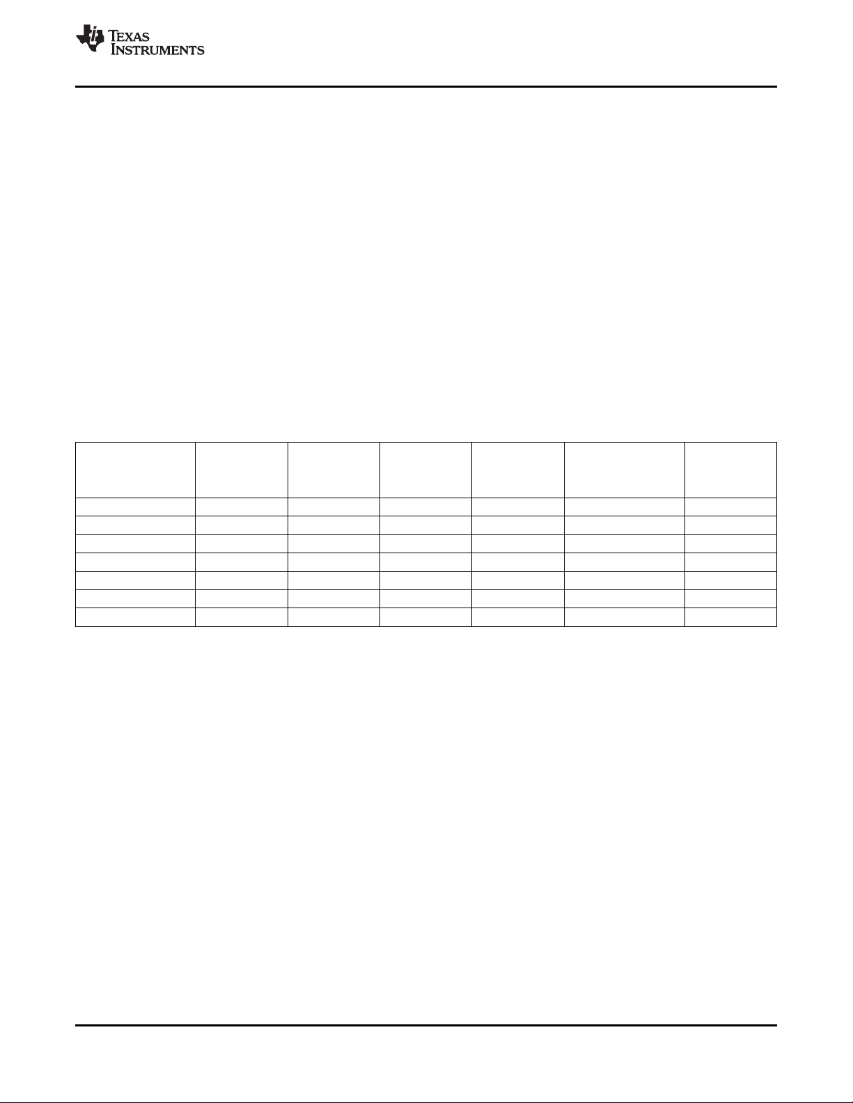
3.4 Color Low-Pass Filter
In some applications, it is desirable to limit the Cb/Cr bandwidth to avoid crosstalk. This is especially true
in case of video signals that have asymmetrical Cb/Cr sidebands. The color LP filters provided limit the
bandwidth of the Cb/Cr signals. Color LP filters are needed when the comb filtering turns off, due to
extreme color transitions in the input image. See Section 3.21.25, Chrominance Control #2 Register, for
the response of these filters. The filters have three options that allow three different frequency responses
based on the color frequency characteristics of the input video as shown in Figure 3-4.
Figure 3-4. Color Low-Pass Filter with Filter Characteristics, NTSC/PAL ITU-R BT.601 Sampling
12 Functional Description Copyright © 2007–2010, Texas Instruments Incorporated
Submit Documentation Feedback
Product Folder Link(s): TVP5150AM1
TVP5150AM1
www.ti.com
3.5 Luminance Processing
The luminance component is derived from the composite signal by subtracting the remodulated
chrominance information. A line delay exists in this path to compensate for the line delay in the adaptive
comb filter in the color processing chain. The luminance information is then fed into the peaking circuit,
which enhances the high frequency components of the signal, thus improving sharpness.
3.6 Chrominance Processing
For NTSC/PAL formats, the color processing begins with a quadrature demodulator. The Cb/Cr signals
then pass through the gain control stage for chrominance saturation adjustment. An adaptive comb filter is
applied to the demodulated signals to separate chrominance and eliminate cross-chrominance artifacts.
An automatic color killer circuit is also included in this block. The color killer suppresses the chrominance
processing when the burst amplitude falls below a programmable threshold (see I2C subaddress 06h). The
SECAM standard is similar to PAL except for the modulation of color which is FM instead of QAM.
3.7 Timing Processor
The timing processor is a combination of hardware and software running in the internal microprocessor
that serves to control horizontal lock to the input sync pulse edge, AGC and offset adjustment in the
analog front end, vertical sync detection, and Macrovision detection.
3.8 VBI Data Processor (VDP)
The TVP5150AM1 VDP slices various data services such as teletext (WST, NABTS), closed captioning
(CC), wide screen signaling (WSS), etc. These services are acquired by programming the VDP to enable
standards in the VBI. The results are stored in a FIFO and/or registers. The teletext results are stored only
in a FIFO. Table 3-1 lists a summary of the types of VBI data supported according to the video standard. It
supports ITU-R BT. 601 sampling for each.
SLES209D–NOVEMBER 2007–REVISED SEPTEMBER 2010
LINE MODE REGISTER
(D0h–FCh) BITS [3:0]
0000b WST SECAM Teletext, SECAM
0001b WST PAL B Teletext, PAL, System B
0010b WST PAL C Teletext, PAL, System C
0011b WST, NTSC B Teletext, NTSC, System B
0100b NABTS, NTSC C Teletext, NTSC, System C
0101b NABTS, NTSC D Teletext, NTSC, System D (Japan)
0110b CC, PAL Closed caption PAL
0111b CC, NTSC Closed caption NTSC
1000b WSS/CGMS-A Wide-screen signaling/Copy Generation Management System-Analog, PAL
1001b WSS/CGMS-A Wide-screen signaling/Copy Generation Management System-Analog, NTSC
1010b VITC, PAL Vertical interval timecode, PAL
1011b VITC, NTSC Vertical interval timecode, NTSC
1100b VPS, PAL Video program system, PAL
1101b Gemstar 2x Custom 1 Electronic program guide
1110b Reserved Reserved
1111b Active Video Active video/full field
Table 3-1. Data Types Supported by VDP
NAME DESCRIPTION
Copyright © 2007–2010, Texas Instruments Incorporated Functional Description 13
Submit Documentation Feedback
Product Folder Link(s): TVP5150AM1
TVP5150AM1
SLES209D–NOVEMBER 2007–REVISED SEPTEMBER 2010
At power-up the host interface is required to program the VDP-configuration RAM (VDP-CRAM) contents
with the lookup table (see Section 3.21.64). This is done through port address C3h. Each read from or
write to this address auto increments an internal counter to the next RAM location. To access the
VDP-CRAM, the line mode registers (D0h to FCh) must be programmed with FFh to avoid a conflict with
the internal microprocessor and the VDP in both writing and reading. Full field mode must also be
disabled.
Available VBI lines are from line 6 to line 27 of both field 1 and field 2. Each line can be any VBI mode.
Output data is available either through the VBI-FIFO (B0h) or through dedicated registers at 90h to AFh,
both of which are available through the I2C port.
3.9 VBI FIFO and Ancillary Data in Video Stream
Sliced VBI data can be output as ancillary data in the video stream in the ITU-R BT.656 mode. VBI data is
output during the horizontal blanking period following the line from which the data was retrieved. Table 3-2
shows the header format and sequence of the ancillary data inserted into the video stream. This format is
also used to store any VBI data into the FIFO. The size of FIFO is 512 bytes. Therefore, the FIFO can
store up to 11 lines of teletext data with the NTSC NABTS standard.
Table 3-2. Ancillary Data Format and Sequence
BYTE NO. D6 D5 D4 D3 D2 D1 DESCRIPTION
0 0 0 0 0 0 0 0 0
1 1 1 1 1 1 1 1 1 Ancillary data preamble
2 1 1 1 1 1 1 1 1
3 NEP EP 0 1 0 DID2 DID1 DID0 Data ID (DID)
4 NEP EP F5 F4 F3 F2 F1 F0 Secondary data ID (SDID)
5 NEP EP N5 N4 N3 N2 N1 N0 Number of 32-bit data (NN)
6 Video line [7:0] Internal data ID0 (IDID0)
7 0 0 0 Match 1 Match 2 Video line [9:8] Internal data ID1 (IDID1)
8 1. Data Data byte
9 2. Data Data byte
10 3. Data Data byte
11 4. Data Data byte
... ... ...
4(N+2)–1 1 0 0 0 0 0 0 0 Fill byte
EP: Even parity for D0–D5
NEP: Negated even parity
DID: 91h: Sliced data of VBI lines of first field
SDID: This field holds the data format taken from the line mode register of the corresponding line.
NN: Number of Dwords beginning with byte 8 through 4(N+2). This value is the number of
IDID0: Transaction video line number [7:0]
D7 D0
(MSB) (LSB)
Data
error
m–1. Data Data byte
m. Data Data byte
RSVD CS[5:0] Check sum
53h: Sliced data of line 24 to end of first field
55h: Sliced data of VBI lines of second field
97h: Sliced data of line 24 to end of second field
Dwords where each Dword is 4 bytes.
www.ti.com
First word
Nthword
14 Functional Description Copyright © 2007–2010, Texas Instruments Incorporated
Submit Documentation Feedback
Product Folder Link(s): TVP5150AM1
TVP5150AM1
www.ti.com
SLES209D–NOVEMBER 2007–REVISED SEPTEMBER 2010
IDID1: Bit 0/1 = Transaction video line number [9:8]
Bit 2 = Match 2 flag
Bit 3 = Match 1 flag
Bit 4 = 1 if an error was detected in the EDC block; 0 if not
CS: Sum of D0–D7 of DID through last data byte.
Fill byte: Fill bytes make a multiple of 4 bytes from byte 0 to last fill byte.
3.10 Raw Video Data Output
The TVP5150AM1 decoder can output raw A/D video data at 2x sampling rate for external VBI slicing.
This is transmitted as an ancillary data block during the active horizontal portion of the line and during
vertical blanking.
3.11 Output Formatter
The YCbCr digital output can be programmed as 8-bit 4:2:2 or 8-bit ITU-R BT.656 parallel interface
standard.
Table 3-3. Summary of Line Frequencies, Data Rates, and Pixel Counts
STANDARDS PIXELS PER LINES PER SUB-CARRIER
(ITU-R BT.601) LINE FRAME FREQUENCY
NTSC-J, M 858 720 525 13.5 3.579545 15.73426
NTSC-4.43 858 720 525 13.5 4.43361875 15.73426
PAL-M 858 720 525 13.5 3.57561149 15.73426
PAL-B, D, G, H, I 864 720 625 13.5 4.43361875 15.625
PAL-N 864 720 625 13.5 4.43361875 15.625
PAL-Nc 864 720 625 13.5 3.58205625 15.625
SECAM 864 720 625 13.5 4.40625/4.25 15.625
ACTIVE PIXEL HORIZONTAL
PIXELS PER FREQUENCY LINE RATE
LINE (MHz) (kHz)
COLOR
(MHz)
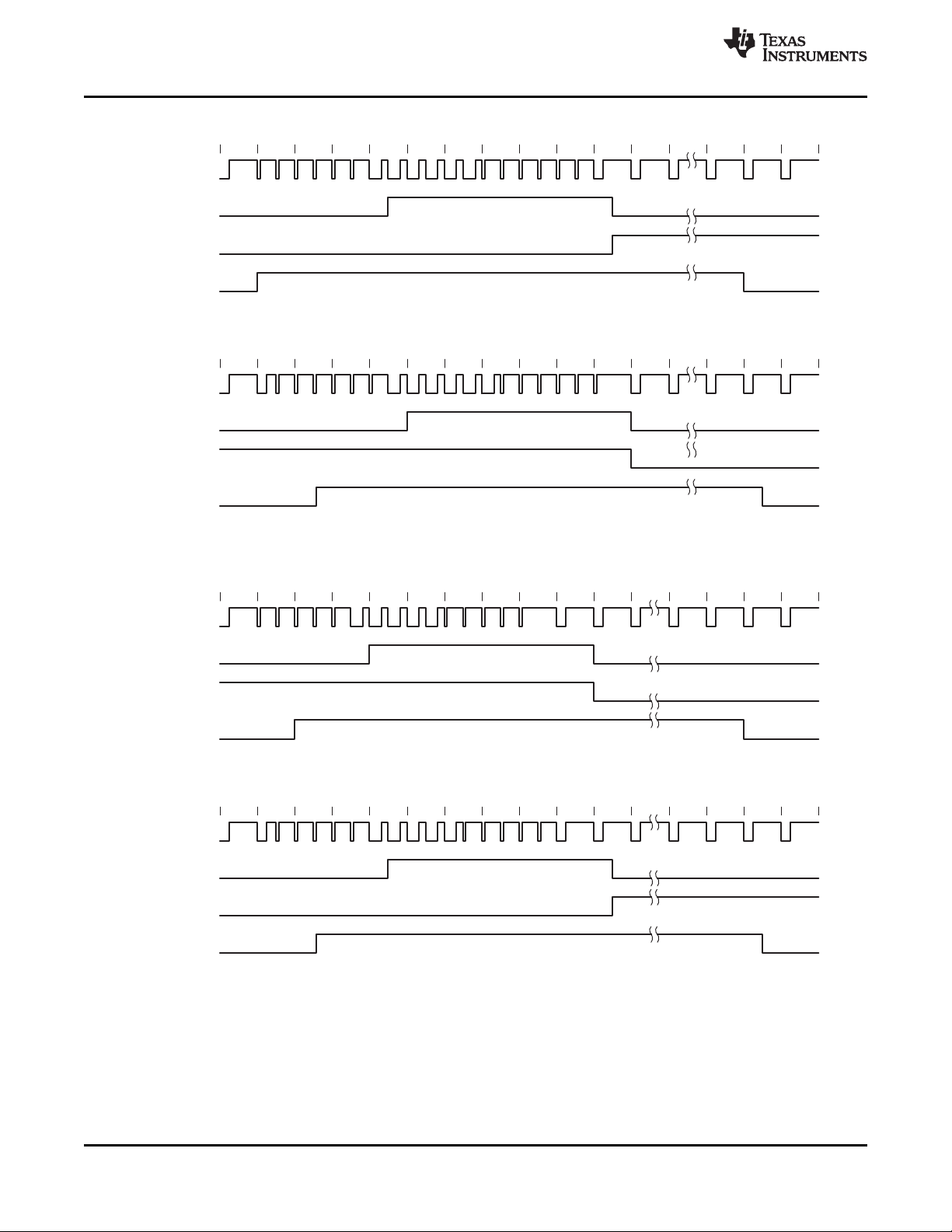
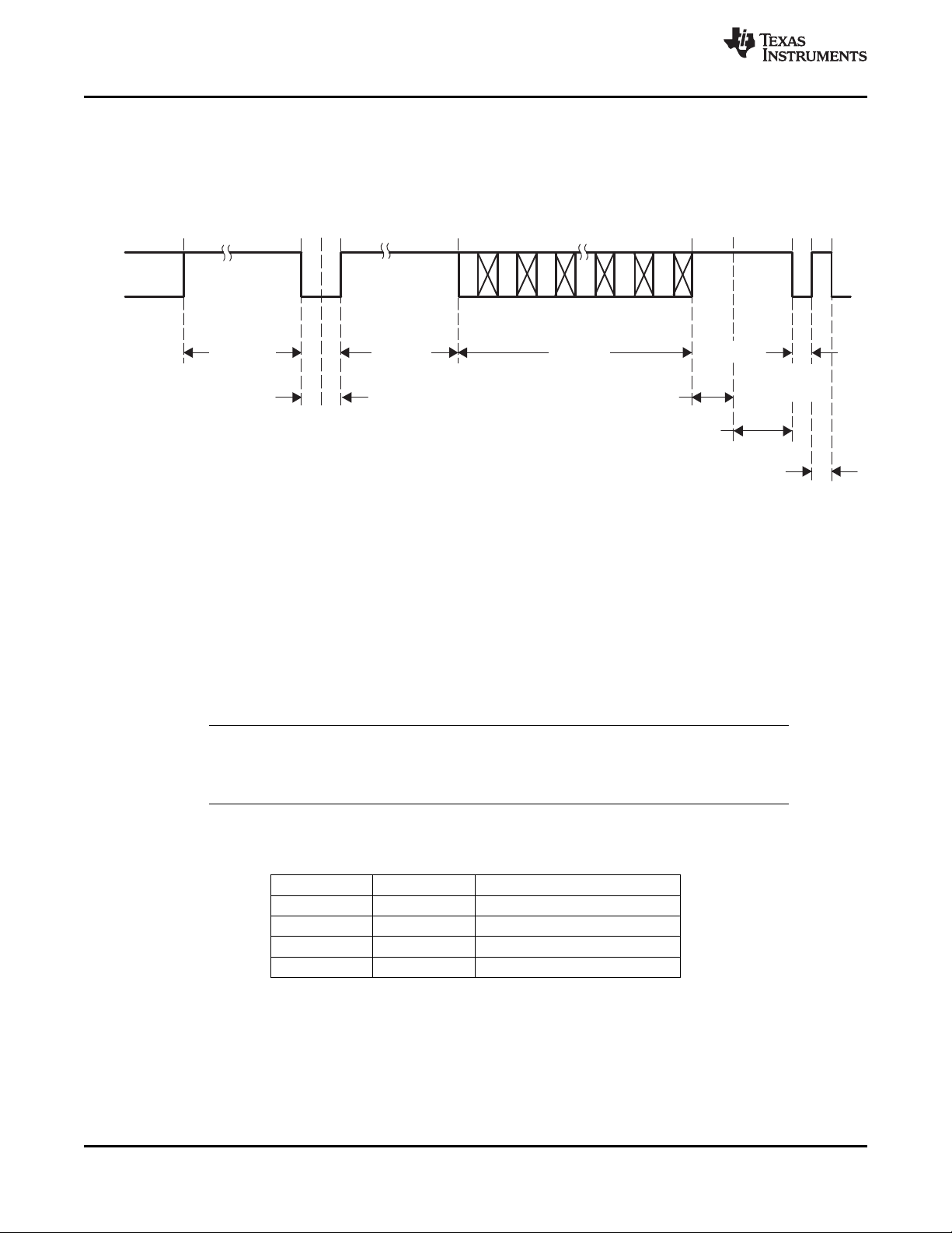
3.12 Synchronization Signals
External (discrete) syncs are provided via the following signals (see Figure 3-5 and Figure 3-6):
• VSYNC (vertical sync)
• FID/VLK (field indicator or vertical lock indicator)
• GPCL/VBLK (general-purpose output or vertical blanking indicator)
• PALI/HLK (PAL switch indicator or horizontal lock indicator)
• HSYNC (horizontal sync)
• AVID (active video indicator) (if set as output)
The position and duration of the HSYNC, VSYNC, VBLK, and AVID outputs are I2C programmable,
providing control of synchronization timing relative to the video output.
Copyright © 2007–2010, Texas Instruments Incorporated Functional Description 15
Submit Documentation Feedback
Product Folder Link(s): TVP5150AM1
Composite
Video
525
VSYNC
GPCL/VBLK
FID
1 2 3 4 5 6 7 8 9 10 11 20 21 22
525 Line
262 263 264 265 266 267 268 269 270 271 272 273 282 283 284
310 311 312 313 314 315 316 317 318 319 320 333 334 335 336
622 623 624 625 1 2 3 4 5 6 7 20 21 22 23
625 Line
Composite
Video
VSYNC
GPCL/VBLK
FID
Composite
Video
VSYNC
GPCL/VBLK
FID
Composite
Video
VSYNC
GPCL/VBLK
FID
↔
VBLK Start
↔
VBLK Stop
↔
VBLK Start
↔
VBLK Stop
↔
VBLK Start
↔
VBLK Stop
↔
VBLK Start
↔
VBLK Stop
TVP5150AM1
SLES209D–NOVEMBER 2007–REVISED SEPTEMBER 2010
www.ti.com
A. Line numbering conforms to ITU-R BT.470 and ITU-R BT.1700.
Figure 3-5. 8-Bit 4:2:2, Timing With 2× Pixel Clock (SCLK) Reference
16 Functional Description Copyright © 2007–2010, Texas Instruments Incorporated
Submit Documentation Feedback
Product Folder Link(s): TVP5150AM1
NTSC 601 1436
PAL 601 1436
ITU 656
Datastream
Cb
359
1437
1437
Y
718
1438
1438
Cr
359
1439
1439
Y
719
1440
1440
FF
1441
1441
00
1455
1459
10
1456
1460
80
HSYNC
AVID
ITU-R BT.656Timing
1583
1587
10
1584
1588
80
1711
1723
10
1712
1724
FF
1713
1725
00
1714
1726
00
1715
1727
XX
0
0
Cb
0
1
1
Y
0
2
2
Cr
0
3
3
Y
1
↔
AVID Stop
↔
AVID Start
↔
HSYNC Start
SECAM
1436 1437 1438 1439 1440
1441
1479 1480 1607 1608 1719 1720
1721 1722
1723
17241725172617
27
…
…
…
…
…
…
TVP5150AM1
www.ti.com
A. AVID rising edge occurs four SCLK cycles early when in the ITU-R BT.656 output mode.
Figure 3-6. Horizontal Synchronization Signals
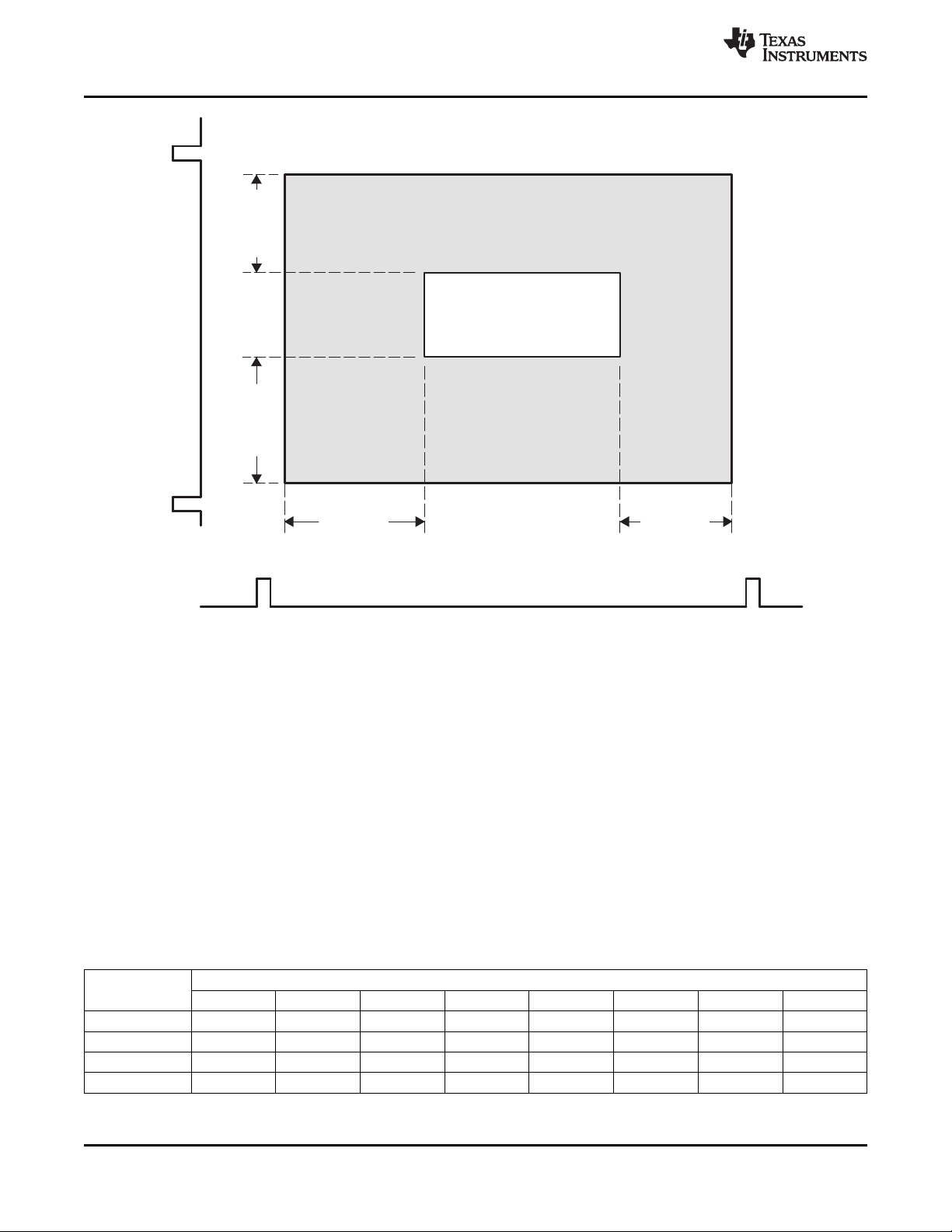
3.13 Active Video (AVID) Cropping
The AVID output signal provides a means to qualify and crop active video both horizontally and vertically.
The horizontal start and stop position of the AVID signal is controlled using registers 11h-12h and
13h-14h, respectively. These registers also control the horizontal position of the embedded sync SAV/EAV
codes.
SLES209D–NOVEMBER 2007–REVISED SEPTEMBER 2010
AVID vertical timing is controlled by the VBLK start and stop registers at addresses 18h and 19h. These
VBLK registers have no effect on the embedded vertical sync code timing. Figure 3-7 shows an AVID
application.
NOTE
The above settings alter AVID output timing, but the video output data is not forced to black
level outside of the AVID interval.
Copyright © 2007–2010, Texas Instruments Incorporated Functional Description 17
Submit Documentation Feedback
Product Folder Link(s): TVP5150AM1
HSYNC
AVID Start AVID Stop
VBLK Stop
VBLK Start
VSYNC
AVID Cropped
Area
Active Video Area
TVP5150AM1
SLES209D–NOVEMBER 2007–REVISED SEPTEMBER 2010
www.ti.com
Figure 3-7. AVID Application
3.14 Embedded Syncs
Standards with embedded syncs insert SAV and EAV codes into the datastream at the beginning and end
of horizontal blanking. These codes contain the V and F bits that also define vertical timing. F and V
change on EAV. Table 3-4 gives the format of the SAV and EAV codes.
H equals 1 always indicates EAV. H equals 0 always indicates SAV. The alignment of V and F to the line
and field counter varies depending on the standard. See ITU-R BT.656 for more information on embedded
syncs.
The P bits are protection bits:
P3 = V xor H
P2 = F xor H
P1 = F xor V
P0 = F xor V xor H
D7 (MSB) D6 D5 D4 D3 D2 D1 D0
Preamble 1 1 1 1 1 1 1 1
Preamble 0 0 0 0 0 0 0 0
Preamble 0 0 0 0 0 0 0 0
Status word 1 F V H P3 P2 P1 P0
Table 3-4. EAV and SAV Sequence
8-BIT DATA
18 Functional Description Copyright © 2007–2010, Texas Instruments Incorporated
Submit Documentation Feedback
Product Folder Link(s): TVP5150AM1
TVP5150AM1
www.ti.com
3.15 I2C Host Interface
The I2C standard consists of two signals, serial input/output data line (SDA) and input/output clock line
(SCL), which carry information between the devices connected to the bus. A third signal (I2CSEL) is used
for slave address selection. Although the I2C system can be multimastered, the TVP5150AM1 decoder
functions only as a slave device.
Both SDA and SCL must be connected to a positive supply voltage via a pullup resistor. When the bus is
free, both lines are high. The slave address select terminal (I2CSEL) enables the use of two
TVP5150AM1 decoders tied to the same I2C bus. At power up, the status of the I2CSEL is polled.
Depending on the write and read addresses to be used for the TVP5150AM1 decoder, it can either be
pulled low or high through a resistor. This terminal is multiplexed with YOUT7 and hence must not be tied
directly to ground or IO_DVDD. Table 3-6 summarizes the terminal functions of the I2C-mode host
interface.
SLES209D–NOVEMBER 2007–REVISED SEPTEMBER 2010
Table 3-5. Write Address
Selection
I2CSEL WRITE ADDRESS
0 B8h
1 BAh
Table 3-6. I2C Terminal Description
SIGNAL TYPE DESCRIPTION
I2CSEL (YOUT7) I Slave address selection
SCL I/O (open drain) Input/output clock line
SDA I/O (open drain) Input/output data line
Data transfer rate on the bus is up to 400 kbit/s. The number of interfaces connected to the bus is
dependent on the bus capacitance limit of 400 pF. The data on the SDA line must be stable during the
high period of the SCL except for start and stop conditions. The high or low state of the data line can only
change with the clock signal on the SCL line being low. A high-to-low transition on the SDA line while the
SCL is high indicates an I2C start condition. A low-to-high transition on the SDA line while the SCL is high
indicates an I2C stop condition.
Every byte placed on the SDA must be eight bits long. The number of bytes which can be transferred is
unrestricted. Each byte must be followed by an acknowledge bit. The acknowledge-related clock pulse is
generated by the I2C master.
Copyright © 2007–2010, Texas Instruments Incorporated Functional Description 19
Submit Documentation Feedback
Product Folder Link(s): TVP5150AM1
TVP5150AM1
SLES209D–NOVEMBER 2007–REVISED SEPTEMBER 2010
3.15.1 I2C Write Operation
Data transfers occur utilizing the following illustrated formats.
An I2C master initiates a write operation to the TVP5150AM1 decoder by generating a start condition (S)
followed by the TVP5150AM1 I2C slave address (see the following illustration), in MSB first bit order,
followed by a 0 to indicate a write cycle. After receiving an acknowledge from the TVP5150AM1 decoder,
the master presents the subaddress of the register, or the first of a block of registers it wants to write,
followed by one or more bytes of data, MSB first. The TVP5150AM1 decoder acknowledges each byte
after completion of each transfer. The I2C master terminates the write operation by generating a stop
condition (P).
Step 1 0
I2C Start (master) S
Step 2 7 6 5 4 3 2 1 0
I2C slave address (master) 1 0 1 1 1 0 X 0
Step 3 9
I2C Acknowledge (slave) A
Step 4 7 6 5 4 3 2 1 0
I2C Write register address (master) Addr Addr Addr Addr Addr Addr Addr Addr
Step 5 9
I2C Acknowledge (slave) A
www.ti.com
Step 6 7 6 5 4 3 2 1 0
I2C Write data (master) Data Data Data Data Data Data Data Data
(1)
Step 7
I2C Acknowledge (slave) A
Step 8 0
I2C Stop (master) P
(1) Repeat steps 6 and 7 until all data have been written.
3.15.2 I2C Read Operation
The read operation consists of two phases. The first phase is the address phase. In this phase, an I2C
master initiates a write operation to the TVP5150AM1 decoder by generating a start condition (S) followed
by the TVP5150AM1 I2C slave address, in MSB first bit order, followed by a 0 to indicate a write cycle.
After receiving an acknowledge from the TVP5150AM1 decoder, the master presents the subaddress of
the register or the first of a block of registers it wants to read. After the cycle is acknowledged, the master
terminates the cycle immediately by generating a stop condition (P).
Table 3-7. Read Address
I2CSEL READ ADDRESS
9
Selection
0 B9h
1 BBh
20 Functional Description Copyright © 2007–2010, Texas Instruments Incorporated
Submit Documentation Feedback
Product Folder Link(s): TVP5150AM1
TVP5150AM1
www.ti.com
The second phase is the data phase. In this phase, an I2C master initiates a read operation to the
TVP5150AM1 decoder by generating a start condition followed by the TVP5150AM1 I2C slave address
(see the following illustration of a read operation), in MSB first bit order, followed by a 1 to indicate a read
cycle. After an acknowledge from the TVP5150AM1 decoder, the I2C master receives one or more bytes
of data from the TVP5150AM1 decoder. The I2C master acknowledges the transfer at the end of each
byte. After the last data byte desired has been transferred from the TVP5150AM1 decoder to the master,
the master generates a not acknowledge followed by a stop.
3.15.2.1 Read Phase 1
Step 1 0
I2C Start (master) S
Step 2 7 6 5 4 3 2 1 0
I2C slave address (master) 1 0 1 1 1 0 X 0
Step 3 9
I2C Acknowledge (slave) A
Step 4 7 6 5 4 3 2 1 0
I2C Write register address (master) Addr Addr Addr Addr Addr Addr Addr Addr
Step 5 9
I2C Acknowledge (slave) A
SLES209D–NOVEMBER 2007–REVISED SEPTEMBER 2010
Step 6 0
I2C Stop (master) P
3.15.2.2 Read Phase 2
Step 7 0
I2C Start (master) S
Step 8 7 6 5 4 3 2 1 0
I2C slave address (master) 1 0 1 1 1 0 X 1
Step 9 9
I2C Acknowledge (slave) A
Step 10 7 6 5 4 3 2 1 0
I2C Read data (slave) Data Data Data Data Data Data Data Data
(1)
Step 11
I2C Not Acknowledge (master) A
Step 12 0
I2C Stop (master) P
(1) Repeat steps 10 and 11 for all bytes read. Master does not acknowledge the last read data received.
9
Copyright © 2007–2010, Texas Instruments Incorporated Functional Description 21
Submit Documentation Feedback
Product Folder Link(s): TVP5150AM1
TVP5150AM1
5
XTAL1
14.31818-MHz
Crystal
6
XTAL2
TVP5150AM1
5
XTAL1
6
XTAL2
C
L1
C
L2
14.31818-MHz
TTL Clock
R
TVP5150AM1
SLES209D–NOVEMBER 2007–REVISED SEPTEMBER 2010
3.15.2.3 I2C Timing Requirements
The TVP5150AM1 decoder requires delays in the I2C accesses to accommodate its internal processor's
timing. In accordance with I2C specifications, the TVP5150AM1 decoder holds the I2C clock line (SCL) low
to indicate the wait period to the I2C master. If the I2C master is not designed to check for the I2C clock
line held-low condition, then the maximum delays must always be inserted where required. These delays
are of variable length; maximum delays are indicated in the following diagram:
Normal register writing addresses 00h to 8Fh (addresses 90h to FFh do not require delays).
Start address Ack Subaddress Ack Data (XXh) Ack Wait 64 µs Stop
Slave
(B8h)
The 64-µs delay is for all registers that do not require a reinitialization. Delays may be more for some
registers.
3.16 Clock Circuits
An internal line-locked PLL generates the system and pixel clocks. A 14.31818-MHz clock is required to
drive the PLL. This may be input to the TVP5150AM1 decoder on terminal 5 (XTAL1), or a crystal of
14.31818-MHz fundamental resonant frequency may be connected across terminals 5 and 6 (XTAL2).
Figure 3-8 shows the reference clock configurations. For the example crystal circuit shown (a
parallel-resonant crystal with 14.31818-MHz fundamental frequency), the external capacitors must have
the following relationship:
CL1= CL2= 2CL– C
where C
is the terminal capacitance with respect to ground, and CLis the crystal load capacitance
STRAY
specified by the crystal manufacturer.
STRAY
www.ti.com
Figure 3-8 shows the reference clock configurations.
NOTE: The resistor (R) in parallel with the crystal is recommended to support a wide range of crystal types. A 100-kΩ resistor
may be used for most crystal types.
Figure 3-8. Reference Clock Configurations
Clock source frequency should have an accuracy of ±50 ppm (max).
22 Functional Description Copyright © 2007–2010, Texas Instruments Incorporated
Submit Documentation Feedback
Product Folder Link(s): TVP5150AM1
SCLK
GLCO
23-Bit Frequency Control
Start Bit DCO Reset Bit
MSB
>128 SCLK
1 SCLK
7 SCLK23 SCLK
1 SCLK
LSB
22 21
0
TVP5150AM1
www.ti.com
3.17 Genlock Control (GLCO) and RTC
A Genlock control function is provided to support a standard video encoder to synchronize its internal
color oscillator for properly reproduced color with unstable timebase sources such as VCRs.
The frequency control word of the internal color subcarrier digitally tuned oscillator (DTO) and the
subcarrier phase reset bit are transmitted via terminal 23 (GLCO). The frequency control word is a 23-bit
binary number. The frequency of the DTO can be calculated from the following equation:
f
= (f
dto
where f
/223) × f
ctrl
dto
sclk
is the frequency of the DTO, f
the SCLK.
3.17.1 GLCO Interface
A write of 1 to bit 4 of the chrominance control register at I2C subaddress 1Ah causes the subcarrier DTO
phase reset bit to be sent on the next scan line on GLCO. The active-low reset bit occurs seven SCLKs
after the transmission of the last bit of DTO frequency control. Upon the transmission of the reset bit, the
phase of the TVP5150AM1 internal subcarrier DTO is reset to zero.
A Genlock slave device can be connected to the GLCO terminal and uses the information on GLCO to
synchronize its internal color phase DTO to achieve clean line and color lock.
Figure 3-9 shows the timing diagram of the GLCO mode.
SLES209D–NOVEMBER 2007–REVISED SEPTEMBER 2010
is the 23-bit DTO frequency control, and f
ctrl
is the frequency of
sclk
Copyright © 2007–2010, Texas Instruments Incorporated Functional Description 23
Figure 3-9. GLCO Timing
Product Folder Link(s): TVP5150AM1
Submit Documentation Feedback
RTC
M
S
B
16 CLK
L
S
B
21 0
128 CLK
22-Bit Fsc Frequency Control
Start
Bit
Reset
Bit
2 CLK
1 CLK
2 CLK
3 CLK
1 CLK
PAL
Switch
44 CLK
TVP5150AM1
SLES209D–NOVEMBER 2007–REVISED SEPTEMBER 2010
3.17.2 RTC Mode
Figure 3-10 shows the timing diagram of the RTC mode. Clock rate for the RTC mode is four times slower
than the GLCO clock rate. For Color PLL frequency control, the upper 22 bits are used. Each frequency
control bit is two clock cycles long. The active-low reset bit occurs six CLKs after the transmission of the
last bit of PLL frequency control.
www.ti.com
Figure 3-10. RTC Timing
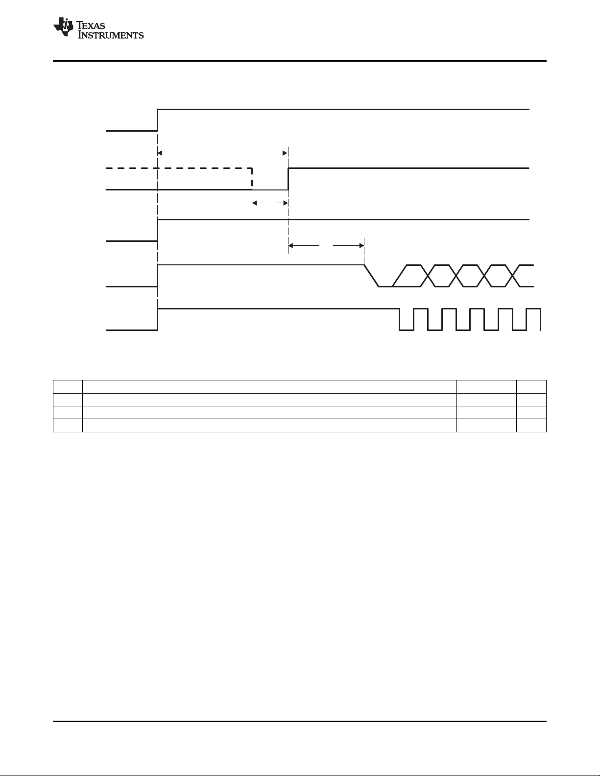
3.18 Reset and Power Down
The RESETB and PDN terminals work together to put the TVP5150AM1 decoder into one of the two
modes. Table 3-8 shows the configuration.
After power-up, the device is in an unknown state with its outputs undefined, until it receives a RESETB
signal as depicted in Figure 3-11. After RESETB is released, the data (YOUT0 to YOUT7) and sync
(HSYNC, VSYNC/PALI) outputs are in high-impedance state until the TVP5150AM1 is initialized and the
outputs are activated.
I2C SCL and SDA signals must not change state until the TVP5150AM1 reset sequence has
been completed.
PDN RESETB CONFIGURATION
NOTE
Table 3-8. Reset and Power-Down Modes
0 0 Reserved (unknown state)
0 1 Powers down the decoder
1 0 Resets the decoder
1 1 Normal operation
24 Functional Description Copyright © 2007–2010, Texas Instruments Incorporated
Submit Documentation Feedback
Product Folder Link(s): TVP5150AM1
RESETB
Normal Operation
Reset
PLL_AVDD
DVDD
IO_DVDD
SDA
PDN
SCL
Data
t1
t2
t3
TVP5150AM1
www.ti.com
After RESETB is released, outputs SCLK and YOUT0 to YOUT7 are high-impedance until the chip is
initialized and the outputs are activated.
SLES209D–NOVEMBER 2007–REVISED SEPTEMBER 2010
Figure 3-11. Power-On Reset Timing
Table 3-9. Power-On Reset Timing
NO. PARAMETER MIN MAX UNIT
t1 Delay time between power supplies active and reset 20 ms
t2 RESETB pulse duration 500 ns
t3 Delay time between end of reset to I2C active 200 µs
Copyright © 2007–2010, Texas Instruments Incorporated Functional Description 25
Submit Documentation Feedback
Product Folder Link(s): TVP5150AM1
TVP5150AM1
SLES209D–NOVEMBER 2007–REVISED SEPTEMBER 2010
www.ti.com
3.19 Reset Sequence
Table 3-10 shows the reset sequence of the TVP5150AM1 pins status during reset time and immediately
after reset time.
Table 3-10. Reset Sequence
PIN DESCRIPTION DURING RESETB
AVID, HSYNC, INTREQ/GPCL/VBLK, VSYNC/PALI, YOUT[0:6] High-impedance High-impedance
AIP1A, AIP1B, RESETB, PDN, SDA, SCL, XTAL1/OSC Input Input
FID/GLCO, PCLK/SCLK, XTAL2 Output Output
YOUT7/I2CSEL Input High-impedance
IMMEDIATELY AFTER
RESETB
26 Functional Description Copyright © 2007–2010, Texas Instruments Incorporated
Submit Documentation Feedback
Product Folder Link(s): TVP5150AM1
TVP5150AM1
www.ti.com
SLES209D–NOVEMBER 2007–REVISED SEPTEMBER 2010
3.20 Internal Control Registers
The TVP5150AM1 decoder is initialized and controlled by a set of internal registers that set all device
operating parameters. Communication between the external controller and the TVP5150AM1 decoder is
through I2C. Table 3-11 shows the summary of these registers. The reserved registers must not be
written. Reserved bits in the defined registers must be written with zeros, unless otherwise noted. The
detailed programming information of each register is described in the following sections.
Table 3-11. Register Summary
REGISTER ADDRESS DEFAULT R/W
Video input source selection #1 00h 00h R/W
Analog channel controls 01h 15h R/W
Operation mode controls 02h 00h R/W
Miscellaneous controls 03h 01h R/W
Autoswitch mask 04h DCh R/W
Reserved 05h 00h R/W
Color killer threshold control 06h 10h R/W
Luminance processing control #1 07h 60h R/W
Luminance processing control #2 08h 00h R/W
Brightness control 09h 80h R/W
Color saturation control 0Ah 80h R/W
Hue control 0Bh 00h R/W
Contrast Control 0Ch 80h R/W
Outputs and data rates select 0Dh 47h R/W
Luminance processing control #3 0Eh 00h R/W
Configuration shared pins 0Fh 08h R/W
Reserved 10h
Active video cropping start pixel MSB 11h 00h R/W
Active video cropping start pixel LSB 12h 00h R/W
Active video cropping stop pixel MSB 13h 00h R/W
Active video cropping stop pixel LSB 14h 00h R/W
Genlock and RTC 15h 01h R/W
Horizontal sync start 16h 80h R/W
Reserved 17h
Vertical blanking start 18h 00h R/W
Vertical blanking stop 19h 00h R/W
Chrominance control #1 1Ah 0Ch R/W
Chrominance control #2 1Bh 14h R/W
Interrupt reset register B 1Ch 00h R/W
Interrupt enable register B 1Dh 00h R/W
Interrupt configuration register B 1Eh 00h R/W
Reserved 1Fh-20h
Indirect Register Data 21h-22h 00h R/W
Indirect Register Address 23h 00h R/W
Indirect Register Read/Write Strobe 24h 00h R/W
Reserved 25h-27h
Video standard 28h 00h R/W
Reserved 29h–2Bh
Cb gain factor 2Ch R
(1) R = Read only, W = Write only, R/W = Read and write
Copyright © 2007–2010, Texas Instruments Incorporated Functional Description 27
Submit Documentation Feedback
Product Folder Link(s): TVP5150AM1
(1)

TVP5150AM1
SLES209D–NOVEMBER 2007–REVISED SEPTEMBER 2010
Table 3-11. Register Summary (continued)
REGISTER ADDRESS DEFAULT R/W
Cr gain factor 2Dh R
Macrovision on counter 2Eh 0Fh R/W
Macrovision off counter 2Fh 01h R/W
656 revision select 30h 00h R/W
Reserved 31h–7Dh
Patch Write Address 7Eh 00h R/W
Patch Code Execute 7Fh 00h R/W
Device ID MSB 80h 51h R
Device ID LSB 81h 50h R
ROM major version 82h 04h R
ROM minor version 83h 00h R
Vertical line count MSB 84h R
Vertical line count LSB 85h R
Interrupt status register B 86h R
Interrupt active register B 87h R
Status register #1 88h R
Status register #2 89h R
Status register #3 8Ah R
Status register #4 8Bh R
Status register #5 8Ch R
Reserved 8Dh
Patch Read Address 8Eh 00h R/W
Reserved 8Fh
Closed caption data 90h–93h R
WSS/CGMS-A data 94h–99h R
VPS/Gemstar 2x data 9Ah–A6h R
VITC data A7h–AFh R
VBI FIFO read data B0h R
Teletext filter and mask 1 B1h–B5h 00h R/W
Teletext filter and mask 2 B6h–BAh 00h R/W
Teletext filter control BBh 00h R/W
Reserved BCh–BFh
Interrupt status register A C0h 00h R/W
Interrupt enable register A C1h 00h R/W
Interrupt configuration register A C2h 04h R/W
VDP configuration RAM data C3h DCh R/W
VDP configuration RAM address low byte C4h 0Fh R/W
VDP configuration RAM address high byte C5h 00h R/W
VDP status C6h R
FIFO word count C7h R
FIFO interrupt threshold C8h 80h R/W
FIFO reset C9h 00h W
Line number interrupt CAh 00h R/W
Pixel alignment LSB CBh 4Eh R/W
Pixel alignment HSB CCh 00h R/W
FIFO output control CDh 01h R/W
www.ti.com
(1)
(2)
(2)
(2)
(2) These registers are used for firmware patch code and should not be written to or read from during
normal operation.
28 Functional Description Copyright © 2007–2010, Texas Instruments Incorporated
Submit Documentation Feedback
Product Folder Link(s): TVP5150AM1

TVP5150AM1
www.ti.com
SLES209D–NOVEMBER 2007–REVISED SEPTEMBER 2010
Table 3-11. Register Summary (continued)
REGISTER ADDRESS DEFAULT R/W
Reserved CEh
Full field enable CFh 00h R/W
Line mode R/W
Full field mode FCh 7Fh R/W
Reserved FDh–FFh
D0h 00h
D1h–FBh FFh
(1)
Copyright © 2007–2010, Texas Instruments Incorporated Functional Description 29
Submit Documentation Feedback
Product Folder Link(s): TVP5150AM1
TVP5150AM1
SLES209D–NOVEMBER 2007–REVISED SEPTEMBER 2010
3.21 Register Definitions
3.21.1 Video Input Source Selection #1 Register
Address 00h
Default 00h
7 6 5 4 3 2 1 0
Reserved Black output Reserved Channel 1 S-video
Channel 1 source selection
0 = AIP1A selected (default)
1 = AIP1B selected
Table 3-12. Analog Channel and Video Mode Selection
Composite
S-Video x 1
INPUT(S) SELECTED
AIP1A (default) 0 0
AIP1B 1 0
AIP1A (luminance),
AIP1B (chrominance)
ADDRESS 00
BIT 1 BIT 0
source selection
selection
www.ti.com
Black output
0 = Normal operation (default)
1 = Force black screen output (outputs synchronized)
a. Forced to 10h in normal mode
b. Forced to 01h in extended mode
3.21.2 Analog Channel Controls Register
Address 01h
Default 15h
7 6 5 4 3 2 1 0
Reserved 1 0 1 Automatic gain control
Automatic gain control (AGC)
00 = AGC disabled (fixed gain value)
01 = AGC enabled (default)
10 = Reserved
11 = AGC frozen to the previously set value
30 Functional Description Copyright © 2007–2010, Texas Instruments Incorporated
Submit Documentation Feedback
Product Folder Link(s): TVP5150AM1

TVP5150AM1
www.ti.com
SLES209D–NOVEMBER 2007–REVISED SEPTEMBER 2010
3.21.3 Operation Mode Controls Register
Address 02h
Default 00h
7 6 5 4 3 2 1 0
Reserved Color burst TV/VCR mode Composite Color Luminance Power-down
Color burst reference enable
0 = Color burst reference for AGC disabled (default)
1 = Color burst reference for AGC enabled (not recommended)
TV/VCR mode
00 = Automatic mode determined by the internal detection circuit (default)
01 = Reserved
10 = VCR (nonstandard video) mode
11 = TV (standard video) mode
With automatic detection enabled, unstable or nonstandard syncs on the input video forces the
detector into the VCR mode. This turns off the comb filters and turns on the chrominance trap filter.
Composite peak disable
0 = Composite peak protection enabled (default)
1 = Composite peak protection disabled
reference peak disable subcarrier PLL peak disable mode
enable frozen
Color subcarrier PLL frozen
0 = Color subcarrier PLL increments by the internally generated phase increment (default). GLCO pin
outputs the frequency increment.
1 = Color subcarrier PLL stops operating. GLCO pin outputs the frozen frequency increment.
Luminance peak disable
0 = Luminance peak processing enabled (default)
1 = Luminance peak processing disabled
Power-down mode
0 = Normal operation (default)
1 = Power-down mode. A/Ds are turned off and internal clocks are reduced to minimum.
Copyright © 2007–2010, Texas Instruments Incorporated Functional Description 31
Submit Documentation Feedback
Product Folder Link(s): TVP5150AM1

TVP5150AM1
SLES209D–NOVEMBER 2007–REVISED SEPTEMBER 2010
3.21.4 Miscellaneous Controls Register
Address 03h
Default 01h
7 6 5 4 3 2 1 0
VBKO GPCL pin GPCL output Lock status YCbCr output HSYNC, Vertical Clock output
enable (HVLK) enable VSYNC/PALI, blanking on/off enable
(TVPOE) AVID,
FID/GLCO
output enable
VBKO function select
0 = GPCL (default)
1 = VBLK
GPCL (data is output based on state of bit 5)
0 = GPCL outputs 0 (default)
1 = GPCL outputs 1
GPCL output enable
0 = GPCL is inactive (default)
1 = GPCL is output
Note: GPCL output enable must not be programmed to be 0 when register 0Fh bit 1 is 1 (GPCL/VBLK).
www.ti.com
Lock status (HVLK) (configured along with register 0Fh, see Figure 3-12 for the relationship between the
configuration shared pins)
0 = Terminal VSYNC/PALI outputs the PAL indicator (PALI) signal and terminal FID/GLCO outputs the
field ID (FID) signal (default) (if terminals are configured to output PALI and FID in register 0Fh).
1 = Terminal VSYNC/PALI outputs the horizontal lock indicator (HLK) and terminal FID outputs the
vertical lock indicator (VLK) (if terminals are configured to output PALI and FID in register 0Fh).
These are additional functions that are provided for ease of use.
YCbCr output enable
0 = YOUT[7:0] high impedance (default)
1 = YOUT[7:0] active
Note: YOUT7 must be pulled high or low for device I2C address select.
32 Functional Description Copyright © 2007–2010, Texas Instruments Incorporated
Submit Documentation Feedback
Product Folder Link(s): TVP5150AM1

TVP5150AM1
www.ti.com
HSYNC, VSYNC/PALI, active video indicator (AVID), and FID/GLCO output enables
0 = HSYNC, VSYNC/PALI, AVID, and FID/GLCO are high-impedance (default).
1 = HSYNC, VSYNC/PALI, AVID, and FID/GLCO are active.
Note: This control bit has no effect on the FID/GLCO output when it is programmed to output the
GLCO signal (see bit 3 of address 0Fh). When the GLCO signal is selected, the FID/GLCO output is
always active.
Vertical blanking on/off
0 = Vertical blanking (VBLK) off (default)
1 = Vertical blanking (VBLK) on
Clock output enable
0 = SCLK output is high impedance
1 = SCLK output is enabled (default)
Note: To achieve lowest power consumption, outputs placed in the high-impedance state should not be
left floating. A 10-kΩ pulldown resistor is recommended if not driven externally.
Note: When enabling the outputs, ensure the clock output is not accidently disabled.
Table 3-13. Digital Output Control
REGISTER 03h, BIT 3 REGISTER C2h, BIT 2
(TVPOE) (VDPOE)
0 X High impedance After both YCbCr output enable bits are programmed
X 0 High impedance After both YCbCr output enable bits are programmed
1 1 Active After both YCbCr output enable bits are programmed
(1) VDPOE default is 1, and TVPOE default is 0.
SLES209D–NOVEMBER 2007–REVISED SEPTEMBER 2010
(1)
YCbCr OUTPUT NOTES
Copyright © 2007–2010, Texas Instruments Incorporated Functional Description 33
Submit Documentation Feedback
Product Folder Link(s): TVP5150AM1

Pin 24
M
U
X
PALI 0
1
PALI/HLK/HVLK
HLK/HVLK
M
U
X
VSYNC 0
1
VSYNC/PALI/HLK/HVLK
0F(Bit 2)
VSYNC/PALI
Pin 23
M
U
X
VLK/HVLK 1
0
GLCO
FID
M
U
X
FID/VLK/HVLK 0
1
FID/GLCO/VLK/HVLK
0F(Bit 3)
FID/GLCO
03(Bit 4)
HVLK
M
U
X
HLK 0
1HVLK
0F(Bit 4)
LOCK24B
M
U
X
HVLK 1
0VLK
0F(Bit 6)
LOCK23
Pin 27
M
U
X
VBLK 1
0
INTREQ
GPCL
M
U
X
VBLK/GPCL 1
0
INTREQ/GPCL//VBLK
03(Bit 7)
VBKO
0F(Bit 1)
INTREQ/GPCL/VBLK
Pin 9
PCLK
M
U
X
SCLK 0
1
PCLK/SCLK
0F(Bit 0)
SCLK/PCLK
03(Bit 5)
GPCL Ouput Enable
TVP5150AM1
SLES209D–NOVEMBER 2007–REVISED SEPTEMBER 2010
www.ti.com
Figure 3-12. Configuration Shared Pins
NOTE
34 Functional Description Copyright © 2007–2010, Texas Instruments Incorporated
Also see the configuration shared pins register at subaddress 0Fh.
Submit Documentation Feedback
Product Folder Link(s): TVP5150AM1

TVP5150AM1
www.ti.com
SLES209D–NOVEMBER 2007–REVISED SEPTEMBER 2010
3.21.5 Autoswitch Mask Register
Address 04h
Default DCh
7 6 5 4 3 2 1 0
Reserved SEC_OFF N4.43_OFF PALN_OFF PALM_OFF Reserved
N4.43_OFF
0 = NTSC4.43 is unmasked from the autoswitch process. Autoswitch does switch to NTSC4.43.
1 = NTSC4.43 is masked from the autoswitch process. Autoswitch does not switch to NTSC4.43
(default).
PALN_OFF
0 = PAL-N is unmasked from the autoswitch process. Autoswitch does switch to PAL-N.
1 = PAL-N is masked from the autoswitch process. Autoswitch does not switch to PAL-N (default).
PALM_OFF
0 = PAL-M is unmasked from the autoswitch process. Autoswitch does switch to PAL-M.
1 = PAL-M is masked from the autoswitch process. Autoswitch does not switch to PAL-M (default).
SEC_OFF
0 = SECAM is unmasked from the autoswitch process. Autoswitch does switch to SECAM (default).
1 = SECAM is masked from the autoswitch process. Autoswitch does not switch to SECAM.
3.21.6 Color Killer Threshold Control Register
Address 06h
Default 10h
7 6 5 4 3 2 1 0
Reserved Automatic color killer Color killer threshold
Automatic color killer
00 = Automatic mode (default)
01 = Reserved
10 = Color killer enabled, CbCr terminals forced to a zero color state
11 = Color killer disabled
Color killer threshold
11111 = –30 dB (minimum)
10000 = –24 dB (default)
00000 = –18 dB (maximum)
Copyright © 2007–2010, Texas Instruments Incorporated Functional Description 35
Submit Documentation Feedback
Product Folder Link(s): TVP5150AM1

TVP5150AM1
SLES209D–NOVEMBER 2007–REVISED SEPTEMBER 2010
www.ti.com
3.21.7 Luminance Processing Control #1 Register
Address 07h
Default 60h
7 6 5 4 3 2 1 0
2× luminance Pedestal not Disable raw Luminance bypass Luminance signal delay with respect to chrominance signal
output enable present header enabled during
2× luminance output enable
0 = Output depends on bit 4, luminance bypass enabled during vertical blanking (default).
1 = Outputs 2x luminance samples during the entire frame. This bit takes precedence over bit 4.
Pedestal not present
0 = 7.5 IRE pedestal is present on the analog video input signal.
1 = Pedestal is not present on the analog video input signal (default).
Disable raw header
0 = Insert 656 ancillary headers for raw data
1 = Disable 656 ancillary headers and instead force dummy ones (40h) (default)
Luminance bypass enabled during vertical blanking
0 = Disabled. If bit 7, 2× luminance output enable, is 0, normal luminance processing occurs and
YCbCr samples are output during the entire frame (default).
1 = Enabled. If bit 7, 2× luminance output enable, is 0, normal luminance processing occurs and
YCbCr samples are output during VACTIVE and 2× luminance samples are output during VBLK.
Luminance bypass occurs for the duration of the vertical blanking as defined by registers 18h and 19h.
vertical blanking
Luminance bypass occurs for the duration of the vertical blanking as defined by registers 18h and 19h.
Luminance signal delay with respect to chrominance signal in pixel clock increments (range –8 to +7 pixel
clocks)
1111 = –8 pixel clocks delay
1011 = –4 pixel clocks delay
1000 = –1 pixel clocks delay
0000 = 0 pixel clocks delay (default)
0011 = +3 pixel clocks delay
0111 = +7 pixel clocks delay
36 Functional Description Copyright © 2007–2010, Texas Instruments Incorporated
Submit Documentation Feedback
Product Folder Link(s): TVP5150AM1

TVP5150AM1
www.ti.com
SLES209D–NOVEMBER 2007–REVISED SEPTEMBER 2010
3.21.8 Luminance Processing Control #2 Register
Address 08h
Default 00h
7 6 5 4 3 2 1 0
Reserved Luminance filter Reserved Peaking gain Mac AGC control
Luminance filter select
0 = Luminance comb filter enabled (default)
1 = Luminance chrominance trap filter enabled
Peaking gain (sharpness)
00 = 0 (default)
01 = 0.5
10 = 1
11 = 2
Information on peaking frequency:
ITU-R BT.601 sampling rate: all standards
Peaking center frequency is 2.6 MHz.
Mac AGC control
00 = Auto mode
01 = Auto mode
10 = Force Macrovision AGC pulse detection off
11 = Force Macrovision AGC pulse detection on
select
3.21.9 Brightness Control Register
Address 09h
Default 80h
7 6 5 4 3 2 1 0
Brightness[7:0]
Brightness[7:0]: This register works for CVBS and S-Video luminance.
1111 1111 = 255 (bright)
1000 0000 = 128 (default)
0000 0000 = 0 (dark)
The output black level relative to the nominal black level (16 out of 256) as a function of the
Brightness[7:0] setting and the Contrast[7:0] setting is as follows:
Black Level = nominal_black_level + (Brightness[7:0] – 128) + (438 / 4) × (1 - Contrast[7:0] / 128)
Copyright © 2007–2010, Texas Instruments Incorporated Functional Description 37
Submit Documentation Feedback
Product Folder Link(s): TVP5150AM1

TVP5150AM1
SLES209D–NOVEMBER 2007–REVISED SEPTEMBER 2010
3.21.10 Color Saturation Control Register
Address 0Ah
Default 80h
7 6 5 4 3 2 1 0
Saturation[7:0]
Saturation[7:0]: This register works for CVBS and S-Video chrominance.
1111 1111 = 255 (maximum)
1000 0000 = 128 (default)
0000 0000 = 0 (no color)
The total chrominance gain relative to the nominal chrominance gain as a function of the Saturation[7:0]
setting is as follows:
Chrominance Gain = nominal_chrominance_gain × (Saturation[7:0] / 128)
3.21.11 Hue Control Register
Address 0Bh
Default 00h
7 6 5 4 3 2 1 0
Hue control
www.ti.com
Hue control (does not apply to SECAM)
0111 1111 = +180 degrees
0000 0000 = 0 degrees (default)
1000 0000 = –180 degrees
3.21.12 Contrast Control Register
Address 0Ch
Default 80h
7 6 5 4 3 2 1 0
Contrast [7:0]
Contrast [7:0]: This register works for CVBS and S-Video luminance.
1111 1111 – 1101 0000 = Reserved
1100 1111 = 207 (maximum contrast)
1000 0000 = 128 (default)
0000 0000 = 0 (minimum contrast)
The total luminance gain relative to the nominal luminance gain as a function of the Contrast [7:0] setting
is as follows:
Luminance Gain = nominal_luminance_gain × (Contrast[7:0] / 128)
NOTE
Luminance peak processing (see bit 1 of subaddress: 02h) may limit the upper end of the
contrast control range.
38 Functional Description Copyright © 2007–2010, Texas Instruments Incorporated
Submit Documentation Feedback
Product Folder Link(s): TVP5150AM1

TVP5150AM1
www.ti.com
SLES209D–NOVEMBER 2007–REVISED SEPTEMBER 2010
3.21.13 Outputs and Data Rates Select Register
Address 0Dh
Default 47h
7 6 5 4 3 2 1 0
Reserved YCbCr output CbCr code YCbCr data path bypass YCbCr output format
YCbCr output code range
CbCr code format
YCbCr data path bypass
code range format
0 = ITU-R BT.601 coding range (Y ranges from 16 to 235. U and V range from 16 to 240)
1 = Extended coding range (Y, U, and V range from 1 to 254) (default)
0 = Offset binary code (2s complement + 128) (default)
1 = Straight binary code (2s complement)
00 = Normal operation (default)
01 = Decimation filter output connects directly to the YCbCr output pins. This data is similar to the
digitized composite data, but the HBLANK area is replaced with ITU-R BT.656 digital blanking.
10 = Digitized composite (or digitized S-video luminance). A/D output connects directly to YCbCr
output pins.
11 = Reserved
YCbCr output format
000 = 8-bit 4:2:2 YCbCr with discrete sync output
001 = Reserved
010 = Reserved
011 = Reserved
100 = Reserved
101 = Reserved
110 = Reserved
111 = 8-bit ITU-R BT.656 interface with embedded sync output (default)
Copyright © 2007–2010, Texas Instruments Incorporated Functional Description 39
Submit Documentation Feedback
Product Folder Link(s): TVP5150AM1

TVP5150AM1
SLES209D–NOVEMBER 2007–REVISED SEPTEMBER 2010
3.21.14 Luminance Processing Control #3 Register
Address 0Eh
Default 00h
7 6 5 4 3 2 1 0
Reserved Luminance trap filter select
Luminance filter stop band bandwidth (MHz)
00 = No notch (default)
01 = Notch 1
10 = Notch 2
11 = Notch 3
Luminance filter select [1:0] selects one of the four chrominance trap (notch) filters to produce luminance
signal by removing the chrominance signal from the composite video signal. The stopband of the
chrominance trap filter is centered at the chrominance subcarrier frequency with stopband bandwidth
controlled by the two control bits. See the following table for the stopband bandwidths. The WCF bit is
controlled in the chrominance control #2 register, see Section 3.21.25.
WCF FILTER SELECT
00 1.2244
0
1
01 0.8782
10 0.7297
11 0.4986
00 1.4170
01 1.0303
10 0.8438
11 0.5537
NTSC/PAL/SECAM
ITU-R BT.601
www.ti.com
40 Functional Description Copyright © 2007–2010, Texas Instruments Incorporated
Submit Documentation Feedback
Product Folder Link(s): TVP5150AM1

TVP5150AM1
www.ti.com
SLES209D–NOVEMBER 2007–REVISED SEPTEMBER 2010
3.21.15 Configuration Shared Pins Register
Address 0Fh
Default 08h
7 6 5 4 3 2 1 0
Reserved LOCK23 Reserved LOCK24B FID/GLCO VSYNC/PALI INTREQ/GPCL/ SCLK/PCLK
LOCK23 (pin 23) function select
0 = FID (default, if bit 3 is selected to output FID)
1 = Lock indicator (indicates whether the device is locked vertically)
LOCK24B (pin 24) function select
0 = PALI (default, if bit 2 is selected to output PALI)
1 = Lock indicator (indicates whether the device is locked horizontally)
FID/GLCO (pin 23) function select (also see register 03h for enhanced functionality)
0 = FID
1 = GLCO (default)
VSYNC/PALI (pin 24) function select (also see register 03h for enhanced functionality)
0 = VSYNC (default)
1 = PALI
VBLK
INTREQ/GPCL/VBLK (pin 27) function select
0 = INTREQ (default)
1 = GPCL or VBLK depending on bit 7 of register 03h
SCLK/PCLK (pin 9) function select
0 = SCLK (default)
1 = PCLK (1x pixel clock frequency)
See Figure 3-12 for the relationship between the configuration shared pins.
3.21.16 Active Video Cropping Start Pixel MSB Register
Address 11h
Default 00h
7 6 5 4 3 2 1 0
AVID start pixel MSB [9:2]
Active video cropping start pixel MSB [9:2], set this register first before setting register 12h. The
TVP5150AM1 decoder updates the AVID start values only when register 12h is written to. This start pixel
value is relative to the default values of the AVID start pixel.
Copyright © 2007–2010, Texas Instruments Incorporated Functional Description 41
Submit Documentation Feedback
Product Folder Link(s): TVP5150AM1

TVP5150AM1
SLES209D–NOVEMBER 2007–REVISED SEPTEMBER 2010
3.21.17 Active Video Cropping Start Pixel LSB Register
Address 12h
Default 00h
7 6 5 4 3 2 1 0
Reserved AVID active AVID start pixel LSB [1:0]
AVID active
0 = AVID out active in VBLK (default)
1 = AVID out inactive in VBLK
Active video cropping start pixel LSB [1:0]: The TVP5150AM1 decoder updates the AVID start values
only when this register is written to.
AVID start [9:0] (combined registers 11h and 12h)
01 1111 1111 = 511
00 0000 0001 = 1
00 0000 0000 = 0 (default)
11 1111 1111 = –1
10 0000 0000 = –512
NOTE
Adjusting AVID start also adjusts the horizontal position of the embedded sync SAV code.
www.ti.com
3.21.18 Active Video Cropping Stop Pixel MSB Register
Address 13h
Default 00h
7 6 5 4 3 2 1 0
AVID stop pixel MSB [9:2]
Active video cropping stop pixel MSB [9:2], set this register first before setting the register 14h. The
TVP5150AM1 decoder updates the AVID stop values only when register 14h is written to. This stop pixel
value is relative to the default values of the AVID stop pixel.
42 Functional Description Copyright © 2007–2010, Texas Instruments Incorporated
Submit Documentation Feedback
Product Folder Link(s): TVP5150AM1

TVP5150AM1
www.ti.com
SLES209D–NOVEMBER 2007–REVISED SEPTEMBER 2010
3.21.19 Active Video Cropping Stop Pixel LSB Register
Address 14h
Default 00h
7 6 5 4 3 2 1 0
Reserved AVID stop pixel LSB
Active video cropping stop pixel LSB [1:0]: The number of pixels of active video must be an even number.
The TVP5150AM1 decoder updates the AVID stop values only when this register is written to.
AVID stop [9:0] (combined registers 13h and 14h)
01 1111 1111 = 511
00 0000 0001 = 1
00 0000 0000 = 0 (default) (see Figure 3-6 and Figure 3-7)
11 1111 1111 = –1
10 0000 0000 = –512
NOTE
Adjusting AVID stop also adjusts the horizontal position of the embedded sync EAV code.
Copyright © 2007–2010, Texas Instruments Incorporated Functional Description 43
Submit Documentation Feedback
Product Folder Link(s): TVP5150AM1

TVP5150AM1
SLES209D–NOVEMBER 2007–REVISED SEPTEMBER 2010
3.21.20 Genlock and RTC Register
Address 15h
Default 01h
7 6 5 4 3 2 1 0
Reserved F/V bit control Reserved GLCO/RTC
F/V bit control
BIT 5 BIT 4 NUMBER OF LINES F BIT V BIT
Standard ITU-R BT.656 ITU-R BT.656
0 0 Nonstandard even Force to 1 Switch at field boundary
Nonstandard odd Toggles Switch at field boundary
0 1
1 0
1 1 Illegal
GLCO/RTC. The following table shows the different modes.
Standard ITU-R BT.656 ITU-R BT.656
Nonstandard Toggles Switch at field boundary
Standard ITU-R BT.656 ITU-R BT.656
Nonstandard Pulse mode Switch at field boundary
BIT 2 BIT 1 BIT 0 GENLOCK/RTC MODE
0 X 0 GLCO
0 X 1
1 X 0 GLCO
1 X 1 RTC output mode 1
RTC output mode 0
(default)
www.ti.com
All other values are reserved.
Figure 3-9 shows the timing of GLCO, and Figure 3-10 shows the timing of RTC.
44 Functional Description Copyright © 2007–2010, Texas Instruments Incorporated
Submit Documentation Feedback
Product Folder Link(s): TVP5150AM1

U
BT.656 EAV Code
YOUT[7:0]
HSYNC
Y V Y FF0000XY801
0
8010FF0000XYU Y
AVID
128 SCLK
N
hbhs
N
hb
Start of
Digital Line
Start of Digital
Active Line
BT.656 SAV Code
TVP5150AM1
www.ti.com
SLES209D–NOVEMBER 2007–REVISED SEPTEMBER 2010
3.21.21 Horizontal Sync Start Register
Address 16h
Default 80h
7 6 5 4 3 2 1 0
HSYNC start
Horizontal sync (HSYNC) start
1111 1111 = –127 × 4 pixel clocks
1111 1110 = –126 × 4 pixel clocks
1000 0001 = –1 × 4 pixel clocks
1000 0000 = 0 pixel clocks (default)
0111 1111 = 1 × 4 pixel clocks
0111 1110 = 2 × 4 pixel clocks
0000 0000 = 128 × 4 pixel clocks
Figure 3-13. Horizontal Sync
Table 3-14. Clock Delays
(SCLKs)
STANDARD N
NTSC 28 272
PAL 32 284
SECAM 32 284
hbhs
N
hb
Detailed timing information is also available in Section 3.12.
Copyright © 2007–2010, Texas Instruments Incorporated Functional Description 45
Submit Documentation Feedback
Product Folder Link(s): TVP5150AM1

TVP5150AM1
SLES209D–NOVEMBER 2007–REVISED SEPTEMBER 2010
3.21.22 Vertical Blanking Start Register
Address 18h
Default 00h
7 6 5 4 3 2 1 0
Vertical blanking start
Vertical blanking (VBLK) start
0111 1111 = 127 lines after start of vertical blanking interval
0000 0001 = 1 line after start of vertical blanking interval
0000 0000 = Same time as start of vertical blanking interval (default) (see Figure 3-5)
1111 1111 = 1 line before start of vertical blanking interval
1000 0000 = 128 lines before start of vertical blanking interval
Vertical blanking is adjustable with respect to the standard vertical blanking intervals. The setting in this
register determines the timing of the GPCL/VBLK signal when it is configured to output vertical blank (see
register 03h). The setting in this register also determines the duration of the luminance bypass function
(see register 07h).
3.21.23 Vertical Blanking Stop Register
Address 19h
Default 00h
7 6 5 4 3 2 1 0
Vertical blanking stop
www.ti.com
Vertical blanking (VBLK) stop
0111 1111 = 127 lines after stop of vertical blanking interval
0000 0001 = 1 line after stop of vertical blanking interval
0000 0000 = Same time as stop of vertical blanking interval (default) (see Figure 3-5)
1111 1111 = 1 line before stop of vertical blanking interval
1000 0000 = 128 lines before stop of vertical blanking interval
Vertical blanking is adjustable with respect to the standard vertical blanking intervals. The setting in this
register determines the timing of the GPCL/VBLK signal when it is configured to output vertical blank (see
register 03h). The setting in this register also determines the duration of the luminance bypass function
(see register 07h).
46 Functional Description Copyright © 2007–2010, Texas Instruments Incorporated
Submit Documentation Feedback
Product Folder Link(s): TVP5150AM1

TVP5150AM1
www.ti.com
SLES209D–NOVEMBER 2007–REVISED SEPTEMBER 2010
3.21.24 Chrominance Control #1 Register
Address 1Ah
Default 0Ch
7 6 5 4 3 2 1 0
Reserved Color PLL reset Chrominance Chrominance Automatic color gain control
Color PLL reset
0 = Color PLL not reset (default)
1 = Color PLL reset
When a 1 is written to this bit, the color PLL phase is reset to zero and the subcarrier PLL phase reset
bit is transmitted on terminal 23 (GLCO) on the next line (NTSC or PAL).
Chrominance adaptive comb filter enable (ACE)
0 = Disable
1 = Enable (default)
Chrominance comb filter enable (CE)
0 = Disable
1 = Enable (default)
adaptive comb comb filter
filter enable enable (CE)
(ACE)
Automatic color gain control (ACGC)
00 = ACGC enabled (default)
01 = Reserved
10 = ACGC disabled
11 = ACGC frozen to the previously set value
Copyright © 2007–2010, Texas Instruments Incorporated Functional Description 47
Submit Documentation Feedback
Product Folder Link(s): TVP5150AM1

TVP5150AM1
SLES209D–NOVEMBER 2007–REVISED SEPTEMBER 2010
3.21.25 Chrominance Control #2 Register
Address 1Bh
Default 14h
7 6 5 4 3 2 1 0
Reserved WCF Chrominance filter select
Wideband chrominance filter (WCF)
0 = Disable
1 = Enable (default)
Chrominance low pass filter select
00 = No notch (default)
01 = Notch 1
10 = Notch 2
11 = Notch 3
Chrominance output bandwidth (MHz)
WCF FILTER SELECT
00 1.2214
0
1
01 0.8782
10 0.7297
11 0.4986
00 1.4170
01 1.0303
10 0.8438
11 0.5537
NTSC/PAL/SECAM
ITU-R BT.601
www.ti.com
48 Functional Description Copyright © 2007–2010, Texas Instruments Incorporated
Submit Documentation Feedback
Product Folder Link(s): TVP5150AM1

TVP5150AM1
www.ti.com
SLES209D–NOVEMBER 2007–REVISED SEPTEMBER 2010
3.21.26 Interrupt Reset Register B
Address 1Ch
Default 00h
7 6 5 4 3 2 1 0
Software Macrovision Reserved Field rate Line alternation Color lock H/V lock TV/VCR
initialization detect changed changed reset changed reset changed reset changed reset changed reset
reset reset
Interrupt reset register B is used by the external processor to reset the interrupt status bits in interrupt
status register B. Bits loaded with a 1 allow the corresponding interrupt status bit to reset to 0. Bits loaded
with a 0 have no effect on the interrupt status bits.
Software initialization reset
0 = No effect (default)
1 = Reset software initialization bit
Macrovision detect changed reset
0 = No effect (default)
1 = Reset Macrovision detect changed bit
Field rate changed reset
0 = No effect (default)
1 = Reset field rate changed bit
Line alternation changed reset
0 = No effect (default)
1 = Reset line alternation changed bit
Color lock changed reset
0 = No effect (default)
1 = Reset color lock changed bit
H/V lock changed reset
0 = No effect (default)
1 = Reset H/V lock changed bit
TV/VCR changed reset [TV/VCR mode is determined by counting the total number of lines/frame. The
mode switches to VCR for nonstandard number of lines]
0 = No effect (default)
1 = Reset TV/VCR changed bit
Copyright © 2007–2010, Texas Instruments Incorporated Functional Description 49
Submit Documentation Feedback
Product Folder Link(s): TVP5150AM1

TVP5150AM1
SLES209D–NOVEMBER 2007–REVISED SEPTEMBER 2010
3.21.27 Interrupt Enable Register B
Address 1Dh
Default 00h
7 6 5 4 3 2 1 0
Software Macrovision Reserved Field rate Line alternation Color lock H/V lock TV/VCR
initialization detect changed changed changed changed changed changed
occurred
Interrupt enable register B is used by the external processor to mask unnecessary interrupt sources for
interrupt B. Bits loaded with a 1 allow the corresponding interrupt condition to generate an interrupt on the
external pin. Conversely, bits loaded with zeros mask the corresponding interrupt condition from
generating an interrupt on the external pin. This register only affects the external pin, it does not affect the
bits in the interrupt status register. A given condition can set the appropriate bit in the status register and
not cause an interrupt on the external pin. To determine if this device is driving the interrupt pin either
AND interrupt status register B with interrupt enable register B or check the state of interrupt B in the
interrupt B active register.
Software initialization occurred
0 = Disabled (default)
1 = Enabled
Macrovision detect changed
0 = Disabled (default)
1 = Enabled
www.ti.com
Field rate changed
0 = Disabled (default)
1 = Enabled
Line alternation changed
0 = Disabled (default)
1 = Enabled
Color lock changed
0 = Disabled (default)
1 = Enabled
H/V lock changed
0 = Disabled (default)
1 = Enabled
TV/VCR changed
0 = Disabled (default)
1 = Enabled
50 Functional Description Copyright © 2007–2010, Texas Instruments Incorporated
Submit Documentation Feedback
Product Folder Link(s): TVP5150AM1

TVP5150AM1
www.ti.com
SLES209D–NOVEMBER 2007–REVISED SEPTEMBER 2010
3.21.28 Interrupt Configuration Register B
Address 1Eh
Default 00h
7 6 5 4 3 2 1 0
Reserved Interrupt
Interrupt polarity B
0 = Interrupt B is active low (default).
1 = Interrupt B is active high.
Interrupt polarity B must be the same as interrupt polarity A of Interrupt Configuration Register A at
Address C2h.
Interrupt Configuration Register B is used to configure the polarity of interrupt B on the external interrupt
pin. When the interrupt B is configured for active low, the pin is driven low when active and high
impedance when inactive (open-drain). Conversely, when the interrupt B is configured for active high, it is
driven high for active and driven low for inactive.
Note: An external pullup resistor (4.7kΩ to 10kΩ) is required when the polarity of the external interrupt
terminal (pin 27) is configured as active low.
3.21.29 Indirect Register Data
polarity B
Address 21h-22h
Default 00h
Address 7 6 5 4 3 2 1 0
22h Data[15:8]
21h Data[7:0]
I2C registers 21h and 22h can be used to write data to or read data from indirect registers. See I2C
registers 23h and 24h.
3.21.30 Indirect Register Address
Address 23h
Default 00h
7 6 5 4 3 2 1 0
ADDR[7:0]
ADDR[7:0] = LSB of indirect address
Copyright © 2007–2010, Texas Instruments Incorporated Functional Description 51
Submit Documentation Feedback
Product Folder Link(s): TVP5150AM1

TVP5150AM1
SLES209D–NOVEMBER 2007–REVISED SEPTEMBER 2010
3.21.31 Indirect Register Read/Write Strobe
Address 24h
Default 00h
7 6 5 4 3 2 1 0
R/W[7:0]
This register selects the most significant bits of the indirect register address and performs either an
indirect read or write operation. Data will be written from are read to Indirect Register Data registers
21h-22h.
R/W[7:0]:
01h = read from 00h-1FFh address bank
02h = write to 00h-1FFh address bank
03h = read from 200h-3FFh address bank
04h = write to 200h-3FFh address bank
05h = read from 300h-3FFh address bank
06h = write to 300h-3FFh address bank
3.21.32 Video Standard Register
Address 28h
Default 00h
7 6 5 4 3 2 1 0
Reserved Video standard
www.ti.com
Video standard
0000 = Autoswitch mode (default)
0001 = Reserved
0010 = (M, J) NTSC ITU-R BT.601
0011 = Reserved
0100 = (B, G, H, I, N) PAL ITU-R BT.601
0101 = Reserved
0110 = (M) PAL ITU-R BT.601
0111 = Reserved
1000 = (Combination-N) PAL ITU-R BT.601
1001 = Reserved
1010 = NTSC 4.43 ITU-R BT.601
1011 = Reserved
1100 = SECAM ITU-R BT.601
With the autoswitch code running, the application can force the device to operate in a particular video
standard mode by writing the appropriate value into this register.
52 Functional Description Copyright © 2007–2010, Texas Instruments Incorporated
Submit Documentation Feedback
Product Folder Link(s): TVP5150AM1

TVP5150AM1
www.ti.com
SLES209D–NOVEMBER 2007–REVISED SEPTEMBER 2010
3.21.33 Cb Gain Factor Register
Address 2Ch
7 6 5 4 3 2 1 0
Cb gain factor
This is a read-only register that provides the gain applied to the Cb in the YCbCr data stream.
3.21.34 Cr Gain Factor Register
Address 2Dh
7 6 5 4 3 2 1 0
Cr gain factor
This is a read-only register that provides the gain applied to the Cr in the YCbCr data stream.
3.21.35 Macrovision On Counter Register
Address 2Eh
Default 0Fh
7 6 5 4 3 2 1 0
Macrovision on counter
This register allows the user to determine how many consecutive frames in which the Macrovision AGC
pulses are detected before the decoder decides that the Macrovision AGC pulses are present.
3.21.36 Macrovision Off Counter Register
Address 2Fh
Default 01h
7 6 5 4 3 2 1 0
Macrovision off counter
This register allows the user to determine how many consecutive frames in which the Macrovision AGC
pulses are not detected before the decoder decides that the Macrovision AGC pulses are not present.
3.21.37 656 Revision Select Register
Address 30h
Default 00h
7 6 5 4 3 2 1 0
Reserved 656 revision
656 revision select
0 = Adheres to ITU-R BT.656.4 and BT.656.5 timing (default)
1 = Adheres to ITU-R BT.656.3 timing
select
Copyright © 2007–2010, Texas Instruments Incorporated Functional Description 53
Submit Documentation Feedback
Product Folder Link(s): TVP5150AM1

TVP5150AM1
SLES209D–NOVEMBER 2007–REVISED SEPTEMBER 2010
3.21.38 Patch Write Address
Address 7Eh
Default 00h
7 6 5 4 3 2 1 0
R/W[7:0]
This register is used for downloading firmware patch code. Please refer to the patch load application note
for more detail. This register must not be written to or read from during normal operation.
3.21.39 Patch Code Execute
Address 7Fh
Default 00h
7 6 5 4 3 2 1 0
R/W[7:0]
Writing to this register following a firmware patch load restarts the CPU and initiates execution of the patch
code. This register must not be written to or read from during normal operation.
3.21.40 MSB of Device ID Register
Address 80h
Default 51h
7 6 5 4 3 2 1 0
MSB of device ID
www.ti.com
This register identifies the MSB of the device ID. Value = 51h.
3.21.41 LSB of Device ID Register
Address 81h
Default 50h
7 6 5 4 3 2 1 0
LSB of device ID
This register identifies the LSB of the device ID. Value = 51h.
54 Functional Description Copyright © 2007–2010, Texas Instruments Incorporated
Submit Documentation Feedback
Product Folder Link(s): TVP5150AM1

TVP5150AM1
www.ti.com
SLES209D–NOVEMBER 2007–REVISED SEPTEMBER 2010
3.21.42 ROM Major Version Register
Address 82h
Default 04h
7 6 5 4 3 2 1 0
ROM major version
This register can contain a number from 01h to FFh.
3.21.43 ROM Minor Version Register
Address 83h
Default 00h
7 6 5 4 3 2 1 0
ROM minor version
This register can contain a number from 01h to FFh.
3.21.44 Vertical Line Count MSB Register
Address 84h
7 6 5 4 3 2 1 0
Reserved Vertical line count MSB
Vertical line count bits [9:8]
3.21.45 Vertical Line Count LSB Register
Address 85h
7 6 5 4 3 2 1 0
Vertical line count LSB
Vertical line count bits [7:0]
Registers 84h and 85h can be read and combined to extract the detected number of lines per frame. This
can be used with nonstandard video signals such as a VCR in fast-forward or rewind modes to
synchronize the downstream video circuitry.
Copyright © 2007–2010, Texas Instruments Incorporated Functional Description 55
Submit Documentation Feedback
Product Folder Link(s): TVP5150AM1

TVP5150AM1
SLES209D–NOVEMBER 2007–REVISED SEPTEMBER 2010
3.21.46 Interrupt Status Register B
Address 86h
7 6 5 4 3 2 1 0
Software Macrovision Reserved Field rate Line alternation Color lock H/V lock TV/VCR
initialization detect changed changed changed changed changed changed
Software initialization
0 = Software initialization is not ready.
1 = Software initialization is ready.
Macrovision detect changed
0 = Macrovision detect status has not changed.
1 = Macrovision detect status has changed.
Field rate changed
0 = Field rate has not changed.
1 = Field rate has changed.
Line alternation changed
0 = Line alteration has not changed.
1 = Line alternation has changed.
www.ti.com
Color lock changed
0 = Color lock status has not changed.
1 = Color lock status has changed.
H/V lock changed
0 = H/V lock status has not changed.
1 = H/V lock status has changed.
TV/VCR changed
0 = TV/VCR status has not changed.
1 = TV/VCR status has changed.
Interrupt status register B is polled by the external processor to determine the interrupt source for interrupt
B. After an interrupt condition is set, it can be reset by writing to the interrupt reset register B at
subaddress 1Ch with a 1 in the appropriate bit.
56 Functional Description Copyright © 2007–2010, Texas Instruments Incorporated
Submit Documentation Feedback
Product Folder Link(s): TVP5150AM1

TVP5150AM1
www.ti.com
SLES209D–NOVEMBER 2007–REVISED SEPTEMBER 2010
3.21.47 Interrupt Active Register B
Address 87h
7 6 5 4 3 2 1 0
Reserved Interrupt B
Interrupt B
0 = Interrupt B is not active on the external terminal (default).
1 = Interrupt B is active on the external terminal.
The interrupt active register B is polled by the external processor to determine if interrupt B is active.
3.21.48 Status Register #1
Address 88h
7 6 5 4 3 2 1 0
Peak white Line-alternating Field rate Lost lock detect Color Vertical sync Horizontal sync TV/VCR status
detect status status status subcarrier lock lock status lock status
Peak white detect status
0 = Peak white is not detected.
1 = Peak white is detected.
status
Line-alternating status
0 = Nonline alternating
1 = Line alternating
Field rate status
0 = 60 Hz
1 = 50 Hz
Lost lock detect
0 = No lost lock since status register #1 was last read.
1 = Lost lock since status register #1 was last read.
Color subcarrier lock status
0 = Color subcarrier is not locked.
1 = Color subcarrier is locked.
Vertical sync lock status
0 = Vertical sync is not locked.
1 = Vertical sync is locked.
Horizontal sync lock status
0 = Horizontal sync is not locked.
1 = Horizontal sync is locked.
TV/VCR status. TV mode is determined by detecting standard line-to-line variations and specific
chrominance SCH phases based on the standard input video format. VCR mode is determined by
detecting variations in the chrominance SCH phases compared to the chrominance SCH phases of the
standard input video format.
0 = TV
1 = VCR
Copyright © 2007–2010, Texas Instruments Incorporated Functional Description 57
Submit Documentation Feedback
Product Folder Link(s): TVP5150AM1

TVP5150AM1
SLES209D–NOVEMBER 2007–REVISED SEPTEMBER 2010
3.21.49 Status Register #2
Address 89h
7 6 5 4 3 2 1 0
Reserved Weak signal PAL switch Field sequence AGC and offset Macrovision detection
detection polarity status frozen status
Weak signal detection
0 = No weak signal
1 = Weak signal mode
PAL switch polarity of first line of odd field
0 = PAL switch is 0.
1 = PAL switch is 1.
Field sequence status
0 = Even field
1 = Odd field
AGC and offset frozen status
0 = AGC and offset are not frozen.
1 = AGC and offset are frozen.
www.ti.com
Macrovision detection
000 = No copy protection
001 = AGC process present (Macrovision Type 1 present)
010 = Colorstripe process Type 2 present
011 = AGC process and colorstripe process Type 2 present
100 = Reserved
101 = Reserved
110 = Colorstripe process Type 3 present
111 = AGC process and color stripe process Type 3 present
58 Functional Description Copyright © 2007–2010, Texas Instruments Incorporated
Submit Documentation Feedback
Product Folder Link(s): TVP5150AM1
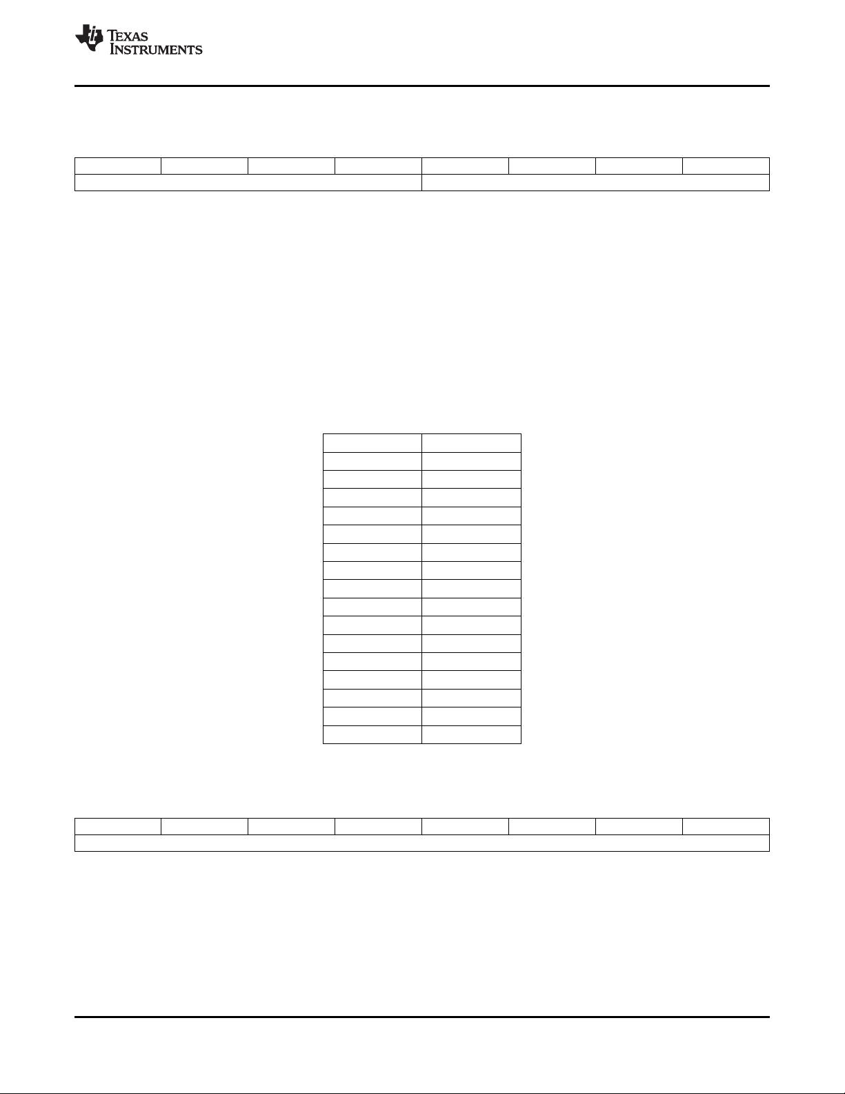
TVP5150AM1
www.ti.com
SLES209D–NOVEMBER 2007–REVISED SEPTEMBER 2010
3.21.50 Status Register #3
Address 8Ah
7 6 5 4 3 2 1 0
Analog gain Digital gain
Analog gain: 4-bit front-end AGC analog gain setting
Digital gain: 4 MSBs of 6-bit front-end AGC digital gain setting
The product of the analog and digital gain is as follows:
Gain Product = (1 + 3 × analog_gain / 15) × (1 + gain_step × digital_gain / 4096)
Where,
0 ≤ analog_gain ≤ 15
0 ≤ digital_gain ≤ 63
The gain_step setting as a function of the analog_gain setting is shown in Table 3-15.
Table 3-15. gain_step Setting
analog_gain gain_step
0 61
1 55
2 48
3 44
4 38
5 33
6 29
7 26
8 24
9 22
10 20
11 19
12 18
13 17
14 16
15 15
3.21.51 Status Register #4
Address 8Bh
7 6 5 4 3 2 1 0
Subcarrier to horizontal (SCH) phase
SCH (color PLL subcarrier phase at 50% of the falling edge of horizontal sync of line one of odd field; step
size 360°/256)
0000 0000 = 0.00°
0000 0001 = 1.41°
0000 0010 = 2.81°
1111 1110 = 357.2°
1111 1111 = 358.6°
Copyright © 2007–2010, Texas Instruments Incorporated Functional Description 59
Submit Documentation Feedback
Product Folder Link(s): TVP5150AM1

TVP5150AM1
SLES209D–NOVEMBER 2007–REVISED SEPTEMBER 2010
www.ti.com
3.21.52 Status Register #5
Address 8Ch
7 6 5 4 3 2 1 0
Autoswitch Reserved Video standard Sampling rate
mode (SR)
This register contains information about the detected video standard at which the device is currently
operating. When autoswitch code is running, this register must be tested to determine which video
standard has been detected.
Autoswitch mode
0 = Forced video standard
1 = Autoswitch mode
Video standard
VIDEO STANDARD [3:1] SR
BIT 3 BIT 2 BIT 1 BIT 0
0 0 0 0 Reserved
0 0 0 1 (M, J) NTSC ITU-R BT.601
0 0 1 0 Reserved
0 0 1 1 (B, D, G, H, I, N) PAL ITU-R BT.601
0 1 0 0 Reserved
0 1 0 1 (M) PAL ITU-R BT.601
0 1 1 0 Reserved
0 1 1 1 PAL-Nc ITU-R BT.601
1 0 0 0 Reserved
1 0 0 1 NTSC 4.43 ITU-R BT.601
1 0 1 0 Reserved
1 0 1 1 SECAM ITU-R BT.601
VIDEO STANDARD
3.21.53 Patch Read Address
Address 8Eh
Default 00h
7 6 5 4 3 2 1 0
R/W[7:0]
This register can be used for patch code read-back. This register must not be written to or read from
during normal operation.
60 Functional Description Copyright © 2007–2010, Texas Instruments Incorporated
Submit Documentation Feedback
Product Folder Link(s): TVP5150AM1
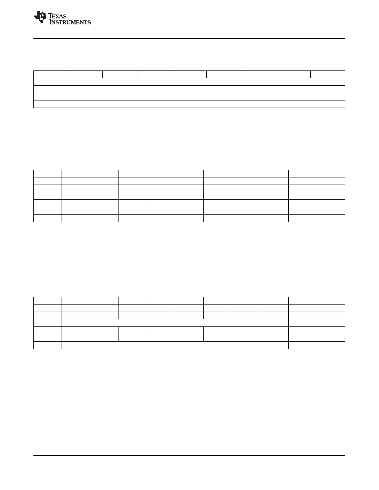
TVP5150AM1
www.ti.com
SLES209D–NOVEMBER 2007–REVISED SEPTEMBER 2010
3.21.54 Closed Caption Data Registers
Address 90h–93h
Address 7 6 5 4 3 2 1 0
90h Closed caption field 1 byte 1
91h Closed caption field 1 byte 2
92h Closed caption field 2 byte 1
93h Closed caption field 2 byte 2
These registers contain the closed caption data arranged in bytes per field.
3.21.55 WSS/CGMS-A Data Registers
Address 94h–99h
NTSC
Address 7 6 5 4 3 2 1 0 BYTE
94h b5 b4 b3 b2 b1 b0 WSS field 1 byte 1
95h b13 b12 b11 b10 b9 b8 b7 b6 WSS field 1 byte 2
96h b19 b18 b17 b16 b15 b14 WSS field 1 byte 3
97h b5 b4 b3 b2 b1 b0 WSS field 2 byte 1
98h b13 b12 b11 b10 b9 b8 b7 b6 WSS field 2 byte 2
99h b19 b18 b17 b16 b15 b14 WSS field 2 byte 3
These registers contain the wide screen signaling (WSS/CGMS-A) data for NTSC.
For NTSC, the bits are:
Bits 0–1 represent word 0, aspect ratio.
Bits 2–5 represent word 1, header code for word 2.
Bits 6–13 represent word 2, copy control.
Bits 14–19 represent word 3, CRC.
PAL/SECAM
Address 7 6 5 4 3 2 1 0 BYTE
94h b7 b6 b5 b4 b3 b2 b1 b0 WSS field 1 byte 1
95h b13 b12 b11 b10 b9 b8 WSS field 1 byte 2
96h Reserved
97h b7 b6 b5 b4 b3 b2 b1 b0 WSS field 2 byte 1
98h b13 b12 b11 b10 b9 b8 WSS field 2 byte 2
99h Reserved
For PAL/SECAM, the bits are:
Bits 0–3 represent group 1, aspect ratio.
Bits 4–7 represent group 2, enhanced services.
Bits 8–10 represent group 3, subtitles.
Bits 11–13 represent group 4, others.
Copyright © 2007–2010, Texas Instruments Incorporated Functional Description 61
Submit Documentation Feedback
Product Folder Link(s): TVP5150AM1
TVP5150AM1
SLES209D–NOVEMBER 2007–REVISED SEPTEMBER 2010
3.21.56 VPS/Gemstar 2x Data Registers
Address 9Ah–A6h
Address 7 6 5 4 3 2 1 0
9Ah VPS/Gemstar 2x byte 1
9Bh VPS/Gemstar 2x byte 2
9Ch VPS/Gemstar 2x byte 3
9Dh VPS/Gemstar 2x byte 4
9Eh VPS/Gemstar 2x byte 5
9Fh VPS/Gemstar 2x byte 6
A0h VPS/Gemstar 2x byte 7
A1h VPS/Gemstar 2x byte 8
A2h VPS/Gemstar 2x byte 9
A3h VPS/Gemstar 2x byte 10
A4h VPS/Gemstar 2x byte 11
A5h VPS/Gemstar 2x byte 12
A6h VPS/Gemstar 2x byte 13
When PAL VPS is used, these registers contain the entire VPS data line except the clock run-in code and
the start code. When NTSC Gemstar 2x is used, these registers contain the Gemstar 2x data.
3.21.57 VITC Data Registers
www.ti.com
Address A7h–AFh
Address 7 6 5 4 3 2 1 0
A7h VITC byte 1, frame byte 1
A8h VITC byte 2, frame byte 2
A9h VITC byte 3, seconds byte 1
AAh VITC byte 4, seconds byte 2
ABh VITC byte 5, minutes byte 1
ACh VITC byte 6, minutes byte 2
ADh VITC byte 7, hour byte 1
AEh VITC byte 8, hour byte 2
AFh VITC byte 9, CRC
These registers contain the VITC data.
3.21.58 VBI FIFO Read Data Register
Address B0h
7 6 5 4 3 2 1 0
FIFO read data
This address is provided to access VBI data in the FIFO through the host port. All forms of teletext data
come directly from the FIFO, while all other forms of VBI data can be programmed to come from the
registers or from the FIFO. Current status of the FIFO can be found at address C6h and the number of
bytes in the FIFO is located at address C7h. If the host port is to be used to read data from the FIFO, then
the host access enable bit at address CDh must be set to 1. The format used for the VBI FIFO is shown in
Section 3.9.
62 Functional Description Copyright © 2007–2010, Texas Instruments Incorporated
Submit Documentation Feedback
Product Folder Link(s): TVP5150AM1
TVP5150AM1
www.ti.com
SLES209D–NOVEMBER 2007–REVISED SEPTEMBER 2010
3.21.59 Teletext Filter and Mask Registers
Address B1h–BAh
Default 00h
Address 7 6 5 4 3 2 1 0
B1h Filter 1 mask 1 Filter 1 pattern 1
B2h Filter 1 mask 2 Filter 1 pattern 2
B3h Filter 1 mask 3 Filter 1 pattern 3
B4h Filter 1 mask 4 Filter 1 pattern 4
B5h Filter 1 mask 5 Filter 1 pattern 5
B6h Filter 2 mask 1 Filter 2 pattern 1
B7h Filter 2 mask 2 Filter 2 pattern 2
B8h Filter 2 mask 3 Filter 2 pattern 3
B9h Filter 2 mask 4 Filter 2 pattern 4
BAh Filter 2 mask 5 Filter 2 pattern 5
For an NABTS system, the packet prefix consists of five bytes. Each byte contains four data bits (D[3:0])
interlaced with four Hamming protection bits (H[3:0]):
7 6 5 4 3 2 1 0
D[3] H[3] D[2] H[2] D[1] H[1] D[0] H[0]
Only the data portion D[3:0] from each byte is applied to a teletext filter function with the corresponding
pattern bits P[3:0] and mask bits M[3:0]. Hamming protection bits are ignored by the filter.
For a WST system (PAL or NTSC), the packet prefix consists of two bytes so that two patterns are used.
Patterns 3, 4, and 5 are ignored.
The mask bits enable filtering using the corresponding bit in the pattern register. For example, a 1 in the
LSB of mask 1 means that the filter module must compare the LSB of nibble 1 in the pattern register to
the first data bit on the transaction. If these match, a true result is returned. A 0 in a bit of mask 1 means
that the filter module must ignore that data bit of the transaction. If all zeros are programmed in the mask
bits, the filter matches all patterns returning a true result (default 00h).
Pattern and mask for each byte and filter are referred as <1,2><P,M><1,2,3,4,5>, where:
<1,2> identifies the filter 1 or 2
<P,M> identifies the pattern or mask
<1,2,3,4,5> identifies the byte number
Copyright © 2007–2010, Texas Instruments Incorporated Functional Description 63
Submit Documentation Feedback
Product Folder Link(s): TVP5150AM1

TVP5150AM1
SLES209D–NOVEMBER 2007–REVISED SEPTEMBER 2010
3.21.60 Teletext Filter Control Register
Address BBh
Default 00h
7 6 5 4 3 2 1 0
Reserved Filter logic Mode TTX filter 2 TTX filter 1
enable enable
Filter logic allows different logic to be applied when combining the decision of filter 1 and filter 2 as follows:
00 = NOR (Default)
01 = NAND
10 = OR
11 = AND
Mode
0 = Teletext WST PAL mode B (2 header bytes) (default)
1 = Teletext NABTS NTSC mode C (5 header bytes)
TTX filter 2 enable
0 = Disabled (default)
1 = Enabled
TTX filter 1 enable
0 = Disabled (default)
1 = Enabled
www.ti.com
If the filter matches or if the filter mask is all zeros, a true result is returned.
64 Functional Description Copyright © 2007–2010, Texas Instruments Incorporated
Submit Documentation Feedback
Product Folder Link(s): TVP5150AM1

TVP5150AM1
www.ti.com
SLES209D–NOVEMBER 2007–REVISED SEPTEMBER 2010
3.21.61 Interrupt Status Register A
Address C0h
Default 00h
7 6 5 4 3 2 1 0
Lock state Lock interrupt Reserved FIFO threshold Line interrupt Data interrupt
interrupt interrupt
The interrupt status register A can be polled by the host processor to determine the source of an interrupt.
After an interrupt condition is set it can be reset by writing to this register with a 1 in the appropriate bit(s).
Lock state interrupt
0 = TVP5150AM1 is not locked to the video signal (default).
1 = TVP5150AM1 is locked to the video signal.
Lock interrupt
0 = A transition has not occurred on the lock signal (default).
1 = A transition has occurred on the lock signal.
FIFO threshold interrupt
0 = The amount of data in the FIFO has not yet crossed the threshold programmed at address C8h
(default).
1 = The amount of data in the FIFO has crossed the threshold programmed at address C8h.
Line interrupt
0 = The video line number has not yet been reached (default).
1 = The video line number programmed in address CAh has occurred.
Data interrupt
0 = No data is available (default).
1 = VBI data is available either in the FIFO or in the VBI data registers.
Copyright © 2007–2010, Texas Instruments Incorporated Functional Description 65
Submit Documentation Feedback
Product Folder Link(s): TVP5150AM1

TVP5150AM1
SLES209D–NOVEMBER 2007–REVISED SEPTEMBER 2010
3.21.62 Interrupt Enable Register A
Address C1h
Default 00h
7 6 5 4 3 2 1 0
Reserved Lock interrupt Reserved FIFO threshold Line interrupt Data interrupt
enable interrupt enable enable enable
The interrupt enable register A is used by the host processor to mask unnecessary interrupt sources. Bits
loaded with a 1 allow the corresponding interrupt condition to generate an interrupt on the external pin.
Conversely, bits loaded with a 0 mask the corresponding interrupt condition from generating an interrupt
on the external pin. This register only affects the interrupt on the external terminal, it does not affect the
bits in interrupt status register A. A given condition can set the appropriate bit in the status register and not
cause an interrupt on the external terminal. To determine if this device is driving the interrupt terminal,
either perform a logical AND of interrupt status register A with interrupt enable register A, or check the
state of the interrupt A bit in the interrupt configuration register at address C2h.
Lock interrupt enable
0 = Disabled (default)
1 = Enabled
FIFO threshold interrupt enable
0 = Disabled (default)
1 = Enabled
www.ti.com
Line interrupt enable
0 = Disabled (default)
1 = Enabled
Data interrupt enable
0 = Disabled (default)
1 = Enabled
66 Functional Description Copyright © 2007–2010, Texas Instruments Incorporated
Submit Documentation Feedback
Product Folder Link(s): TVP5150AM1

TVP5150AM1
www.ti.com
SLES209D–NOVEMBER 2007–REVISED SEPTEMBER 2010
3.21.63 Interrupt Configuration Register A
Address C2h
Default 04h
7 6 5 4 3 2 1 0
Reserved YCbCr enable Interrupt A Interrupt
YCbCr enable (VDPOE)
0 = YCbCr pins are high impedance.
1 = YCbCr pins are active if other conditions are met (default) (see Table 3-13).
Interrupt A (read only)
0 = Interrupt A is not active on the external pin (default).
1 = Interrupt A is active on the external pin.
Interrupt polarity A must be the same as interrupt polarity B of Interrupt Configuration Register B at
Address 1Eh.
Interrupt polarity A
0 = Interrupt A is active low (default).
1 = Interrupt A is active high.
Interrupt configuration register A is used to configure the polarity of the external interrupt terminal. When
interrupt A is configured as active low, the terminal is driven low when active and high impedance when
inactive (open drain). Conversely, when the terminal is configured as active high, it is driven high when
active and driven low when inactive.
(VDPOE) polarity A
Note: An external pullup resistor (4.7kΩ to 10kΩ) is required when the polarity of the external interrupt
terminal (pin 27) is configured as active low.
3.21.64 VDP Configuration RAM Register
Address C3h C4h C5h
Default DCh 0Fh 00h
Address 7 6 5 4 3 2 1 0
C3h Configuration data
C4h RAM address (7:0)
C5h Reserved RAM
The configuration RAM data is provided to initialize the VDP with initial constants. The configuration RAM
is 512 bytes organized as 32 different configurations of 16 bytes each. The first 12 configurations are
defined for the current VBI standards. An additional two configurations can be used as a custom
programmed mode for unique standards such as Gemstar.
Address C3h is used to read or write to the RAM. The RAM internal address counter is automatically
incremented with each transaction. Addresses C5h and C4h make up a 9-bit address to load the internal
address counter with a specific start address. This can be used to write a subset of the RAM for only
those standards of interest.
NOTE
Registers D0h–FBh must all be programmed with FFh before writing or reading the
configuration RAM. Full field mode (CFh) must be disabled as well.
address 8
Copyright © 2007–2010, Texas Instruments Incorporated Functional Description 67
Submit Documentation Feedback
Product Folder Link(s): TVP5150AM1

TVP5150AM1
SLES209D–NOVEMBER 2007–REVISED SEPTEMBER 2010
www.ti.com
The suggested RAM contents are shown in Table 3-16. All values are hexadecimal.
Table 3-16. VBI Configuration RAM for Signals With Pedestal
INDEX ADDRESS 0 1 2 3 4 5 6 7 8 9 A B C D E F
WST SECAM 000 AA AA FF FF E7 2E 20 A6 E4 B4 0E 0 7 0 10 0
WST SECAM 010 AA AA FF FF E7 2E 20 A6 E4 B4 0E 0 7 0 10 0
WST PAL B 020 AA AA FF FF 27 2E 20 AB A4 72 10 0 7 0 10 0
WST PAL B 030 AA AA FF FF 27 2E 20 AB A4 72 10 0 7 0 10 0
WST PAL C 040 AA AA FF FF E7 2E 20 22 A4 98 0D 0 0 0 10 0
WST PAL C 050 AA AA FF FF E7 2E 20 22 A4 98 0D 0 0 0 10 0
WST NTSC 060 AA AA FF FF 27 2E 20 23 63 93 0D 0 0 0 10 0
WST NTSC 070 AA AA FF FF 27 2E 20 23 63 93 0D 0 0 0 10 0
NABTS, NTSC 080 AA AA FF FF E7 2E 20 A2 63 93 0D 0 7 0 15 0
NABTS, NTSC 090 AA AA FF FF E7 2E 20 A2 63 93 0D 0 7 0 15 0
NABTS, NTSC-J 0A0 AA AA FF FF A7 2E 20 A3 63 93 0D 0 7 0 10 0
NABTS, NTSC-J 0B0 AA AA FF FF A7 2E 20 A3 63 93 0D 0 7 0 10 0
CC, PAL/SECAM 0C0 AA 2A FF 3F 04 51 6E 02 A4 7B 09 0 0 0 27 0
CC, PAL/SECAM 0D0 AA 2A FF 3F 04 51 6E 02 A4 7B 09 0 0 0 27 0
CC, NTSC 0E0 AA 2A FF 3F 04 51 6E 02 63 8C 09 0 0 0 27 0
CC, NTSC 0F0 AA 2A FF 3F 04 51 6E 02 63 8C 09 0 0 0 27 0
WSS/CGMS-A,
PAL/SECAM
WSS/CGMS-A,
PAL/SECAM
WSS/CGMS-A,
NTSC C
WSS/CGMS-A,
NTSC C
VITC, PAL/SECAM 140 0 0 0 0 0 8F 6D 49 A4 85 08 0 0 0 4C 0
VITC, PAL/SECAM 150 0 0 0 0 0 8F 6D 49 A4 85 08 0 0 0 4C 0
VITC, NTSC 160 0 0 0 0 0 8F 6D 49 63 94 08 0 0 0 4C 0
VITC, NTSC 170 0 0 0 0 0 8F 6D 49 63 94 08 0 0 0 4C 0
VPS, PAL 180 AA AA FF FF BA CE 2B 8D A4 DA 0B 0 7 0 60 0
VPS, PAL 190 AA AA FF FF BA CE 2B 8D A4 DA 0B 0 7 0 60 0
Gemstar 2x
Custom 1
Gemstar 2x
Custom 1
Custom 2 1C0 Programmable
Custom 2 1D0 Programmable
100 5B 55 C5 FF 0 71 6E 42 A4 CD 0F 0 0 0 3A 0
110 5B 55 C5 FF 0 71 6E 42 A4 CD 0F 0 0 0 3A 0
120 38 00 3F 00 0 71 6E 43 63 7C 08 0 0 0 39 0
130 38 00 3F 00 0 71 6E 43 63 7C 08 0 0 0 39 0
1A0 99 99 FF FF 05 51 6E 05 63 18 13 80 00 00 60 00
1B0 99 99 FF FF 05 51 6E 05 63 18 13 80 00 00 60 00
68 Functional Description Copyright © 2007–2010, Texas Instruments Incorporated
Submit Documentation Feedback
Product Folder Link(s): TVP5150AM1

TVP5150AM1
www.ti.com
SLES209D–NOVEMBER 2007–REVISED SEPTEMBER 2010
3.21.65 VDP Status Register
Address C6h
7 6 5 4 3 2 1 0
FIFO full error FIFO empty TTX available CC field 1 CC field 2 WSS/CGMS-A VPS/Gemstar VITC available
The VDP status register indicates whether data is available in either the FIFO or data registers, and status
information about the FIFO. Reading data from the corresponding register does not clear the status flags
automatically. These flags are only reset by writing a 1 to the respective bit. However, bit 6 is updated
automatically.
FIFO full error
0 = No FIFO full error
1 = FIFO was full during a write to FIFO.
The FIFO full error flag is set when the current line of VBI data can not enter the FIFO. For example, if
the FIFO has only ten bytes left and teletext is the current VBI line, the FIFO full error flag is set, but no
data is written because the entire teletext line does not fit. However, if the next VBI line is closed
caption requiring only two bytes of data plus the header, this goes into the FIFO, even if the full error
flag is set.
FIFO empty
0 = FIFO is not empty.
1 = FIFO is empty.
available available available 2x available
TTX available
0 = Teletext data is not available.
1 = Teletext data is available.
CC field 1 available
0 = Closed caption data from field 1 is not available.
1 = Closed caption data from field 1 is available.
CC field 2 available
0 = Closed caption data from field 2 is not available.
1 = Closed caption data from field 2 is available.
WSS/CGMS-A available
0 = WSS/CGMS-A data is not available.
1 = WSS/CGMS-A data is available.
VPS/Gemstar 2x available
0 = VPS/Gemstar 2x data is not available.
1 = VPS/Gemstar 2x data is available.
VITC available
0 = VITC data is not available.
1 = VITC data is available.
Copyright © 2007–2010, Texas Instruments Incorporated Functional Description 69
Submit Documentation Feedback
Product Folder Link(s): TVP5150AM1

TVP5150AM1
SLES209D–NOVEMBER 2007–REVISED SEPTEMBER 2010
3.21.66 FIFO Word Count Register
Address C7h
7 6 5 4 3 2 1 0
Number of words
This register provides the number of words in the FIFO. One word equals two bytes.
3.21.67 FIFO Interrupt Threshold Register
Address C8h
Default 80h
7 6 5 4 3 2 1 0
Number of words
This register is programmed to trigger an interrupt when the number of words in the FIFO exceeds this
value (default 80h). This interrupt must be enabled at address C1h. One word equals two bytes.
3.21.68 FIFO Reset Register
Address C9h
Default 00h
7 6 5 4 3 2 1 0
Any data
www.ti.com
Writing any data to this register resets the FIFO and clears any data present in all VBI read registers.
3.21.69 Line Number Interrupt Register
Address CAh
Default 00h
7 6 5 4 3 2 1 0
Field 1 enable Field 2 enable Line number
This register is programmed to trigger an interrupt when the video line number matches this value in bits
5:0. This interrupt must be enabled at address C1h. The value of 0 or 1 does not generate an interrupt.
Field 1 enable
0 = Disabled (default)
1 = Enabled
Field 2 enable
0 = Disabled (default)
1 = Enabled
Line number default is 00h.
70 Functional Description Copyright © 2007–2010, Texas Instruments Incorporated
Submit Documentation Feedback
Product Folder Link(s): TVP5150AM1

TVP5150AM1
www.ti.com
SLES209D–NOVEMBER 2007–REVISED SEPTEMBER 2010
3.21.70 Pixel Alignment Registers
Address CBh CCh
Default 4Eh 00h
Address 7 6 5 4 3 2 1 0
CBh Switch pixel [7:0]
CCh Reserved Switch pixel [9:8]
These registers form a 10-bit horizontal pixel position from the falling edge of sync, where the VDP
controller initiates the program from one line standard to the next line standard; for example, the previous
line of teletext to the next line of closed caption. This value must be set so that the switch occurs after the
previous transaction has cleared the delay in the VDP, but early enough to allow the new values to be
programmed before the current settings are required.
3.21.71 FIFO Output Control Register
Address CDh
Default 01h
7 6 5 4 3 2 1 0
Reserved Host access
This register is programmed to allow I2C access to the FIFO or to allow all VDP data to go out the video
port as ancillary data.
enable
Host access enable
0 = Output FIFO data to the video output Y[7:0] as ancillary data
1 = Read FIFO data via I2C register B0h (default)
3.21.72 Full Field Enable Register
Address CFh
Default 00h
7 6 5 4 3 2 1 0
Reserved Full field enable
This register enables the full field mode. In this mode, all lines outside the vertical blank area and all lines
in the line mode registers programmed with FFh are sliced with the definition of register FCh. Values other
than FFh in the line mode registers allow a different slice mode for that particular line.
Full field enable
0 = Disable full field mode (default)
1 = Enable full field mode
Copyright © 2007–2010, Texas Instruments Incorporated Functional Description 71
Submit Documentation Feedback
Product Folder Link(s): TVP5150AM1

TVP5150AM1
SLES209D–NOVEMBER 2007–REVISED SEPTEMBER 2010
3.21.73 Line Mode Registers
Address D0h D1h–FBh
Default 00h FFh
Address 7 6 5 4 3 2 1 0
D0 Line 6 Field 1
D1 Line 6 Field 2
D2 Line 7 Field 1
D3 Line 7 Field 2
D4 Line 8 Field 1
D5 Line 8 Field 2
D6 Line 9 Field 1
D7 Line 9 Field 2
D8 Line 10 Field 1
D9 Line 10 Field 2
DA Line 11 Field 1
DB Line 11 Field 2
DC Line 12 Field 1
DD Line 12 Field 2
DE Line 13 Field 1
DF Line 13 Field 2
E0 Line 14 Field 1
E1 Line 14 Field 2
E2 Line 15 Field 1
E3 Line 15 Field 2
E4 Line 16 Field 1
E5 Line 16 Field 2
E6 Line 17 Field 1
E7 Line 17 Field 2
E8 Line 18 Field 1
E9 Line 18 Field 2
EA Line 19 Field 1
EB Line 19 Field 2
EC Line 20 Field 1
ED Line 20 Field 2
EE Line 21 Field 1
EF Line 21 Field 2
F0 Line 22 Field 1
F1 Line 22 Field 2
F2 Line 23 Field 1
F3 Line 23 Field 2
F4 Line 24 Field 1
F5 Line 24 Field 2
F6 Line 25 Field 1
F7 Line 25 Field 2
F8 Line 26 Field 1
F9 Line 26 Field 2
FA Line 27 Field 1
FB Line 27 Field 2
www.ti.com
These registers program the specific VBI standard at a specific line in the video field.
72 Functional Description Copyright © 2007–2010, Texas Instruments Incorporated
Submit Documentation Feedback
Product Folder Link(s): TVP5150AM1

TVP5150AM1
www.ti.com
Bit 7
Bit 6
Bit 5
Bit 4
Bits [3:0]
SLES209D–NOVEMBER 2007–REVISED SEPTEMBER 2010
0 = Disable filtering of null bytes in closed caption modes
1 = Enable filtering of null bytes in closed caption modes (default)
In teletext modes, bit 7 enables the data filter function for that particular line. If it is set to 0, the data
filter passes all data on that line.
0 = Send VBI data to registers only
1 = Send VBI data to FIFO and the registers. Teletext data only goes to FIFO (default).
0 = Allow VBI data with errors in the FIFO
1 = Do not allow VBI data with errors in the FIFO (default)
0 = Do not enable error detection and correction
1 = Enable error detection and correction (default)
0000 = WST SECAM
0001 = WST PAL B
0010 = WST PAL C
0011 = WST NTSC
0100 = NABTS NTSC
0101 = TTX NTSC-J
0110 = CC PAL
0111 = CC NTSC
1000 = WSS/CGMS-A PAL
1001 = WSS/CGMS-A NTSC
1010 = VITC PAL
1011 = VITC NTSC
1100 = VPS PAL
1101 = Gemstar 2x Custom 1
1110 = Custom 2
1111 = Active video (VDP off) (default)
A value of FFh in the line mode registers is required for any line to be sliced as part of the full field mode.
3.21.74 Full Field Mode Register
Address FCh
Default 7Fh
7 6 5 4 3 2 1 0
Full field mode
This register programs the specific VBI standard for full field mode. It can be any VBI standard. Individual
line settings take priority over the full field register. This allows each VBI line to be programmed
independently but have the remaining lines in full field mode. The full field mode register has the same
definitions as the line mode registers (default 7Fh).
Copyright © 2007–2010, Texas Instruments Incorporated Functional Description 73
Submit Documentation Feedback
Product Folder Link(s): TVP5150AM1
TVP5150AM1
SLES209D–NOVEMBER 2007–REVISED SEPTEMBER 2010
www.ti.com
4 Electrical Specifications
4.1 Absolute Maximum Ratings
over operating free-air temperature range (unless otherwise noted)
Supply voltage range
Digital input voltage range, VIto DGND –0.5 V to 4.5 V
Input voltage range, XTAL1 to PLL_GND –0.5 V to 2.3 V
Analog input voltage range AIto CH_AGND –0.2 V to 2.0 V
Digital output voltage range, VOto DGND –0.5 V to 4.5 V
Operating free-air temperature, T
Storage temperature range, T
(1) Stresses beyond those listed under absolute maximum ratings may cause permanent damage to the device. These are stress ratings
only, and functional operation of the device at these or any other conditions beyond those indicated under recommended operating
conditions is not implied. Exposure to absolute-maximum-rated conditions for extended periods may affect device reliability.
A
stg
4.2 Recommended Operating Conditions
IO_DVDD Digital I/O supply voltage 3.0 3.3 3.6 V
DVDD Digital supply voltage 1.65 1.8 1.95 V
PLL_AVDD Analog PLL supply voltage 1.65 1.8 1.95 V
CH_AVDD Analog core supply voltage 1.65 1.8 1.95 V
V
I(P-P)
V
IH
V
IL
V
IH_XTAL
V
IL_XTAL
I
OH
I
OL
I
OH_SCLK
I
OL_SCLK
T
A
Analog input voltage (ac-coupling necessary) 0 0.75 V
Digital input voltage high 0.7 IO_DVDD V
Digital input voltage low 0.3 IO_DVDD V
XTAL input voltage high 0.7 PLL_AVDD V
XTAL input voltage low 0.3 PLL_AVDD V
High-level output current 2 mA
Low-level output current –2 mA
SCLK high-level output current 4 mA
SCLK low-level output current –4 mA
Operating free-air temperature °C
(1)
IO_DVDD to DGND –0.5 V to 4.5 V
DVDD to DGND –0.5 V to 2.3 V
PLL_AVDD to PLL_AGND –0.5 V to 2.3 V
CH_AVDD to CH_AGND –0.5 V to 2.3 V
Commercial 0°C to 70°C
Industrial –40°C to 85°C
–65°C to 150°C
MIN NOM MAX UNIT
Commercial 0 70
Industrial –40 85
4.3 Reference Clock Specifications
MIN NOM MAX UNIT
f Frequency 14.31818 MHz
Δf Frequency tolerance
(1) Specified by design
74 Electrical Specifications Copyright © 2007–2010, Texas Instruments Incorporated
(1)
–50 +50 ppm
Submit Documentation Feedback
Product Folder Link(s): TVP5150AM1

TVP5150AM1
www.ti.com
SLES209D–NOVEMBER 2007–REVISED SEPTEMBER 2010
4.4 Electrical Characteristics
DVDD = 1.8 V, PLL_AVDD = 1.8 V, CH_AVDD = 1.8 V, IO_DVDD = 3.3 V
For minimum/maximum values TA= 0°C to 70°C for commercial or TA= –40°C to 85°C for industrial, for typical
values TA= 25°C (unless otherwise noted)
4.5 DC Electrical Characteristics
PARAMETER MIN TYP MAX UNIT
I
DD(IO_D)
I
DD(D)
I
DD(PLL_A)
I
DD(CH_A)
P
TOT
P
DOWN
C
i
V
OH
V
OL
V
OH_SCLK
V
OL_SCLK
I
IH
I
IL
3.3-V I/O digital supply current Color bar input
1.8-V digital supply current Color bar input
1.8-V analog PLL supply current Color bar input
1.8-V analog core supply current Color bar input
Total power dissipation, normal mode Color bar input
Total power dissipation, power-down mode
(3)
Input capacitance By design 8 pF
Output voltage high IOH= 2 mA 0.8 IO_DVDD V
Output voltage low IOL= –2 mA 0.22 IO_DVDD V
SCLK output voltage high IOH= 4 mA 0.8 IO_DVDD V
SCLK output voltage low IOL= –4 mA 0.22 IO_DVDD V
High-level input current
Low-level input current
(4)
(4)
(1) Measured with a load of 15 pF
(2) For typical measurements only
(3) Assured by device characterization
(4) YOUT7 is a bidirectional terminal with an internal pulldown resistor. This terminal may sink more than the specified current when in
RESET mode.
TEST
CONDITIONS
(1)
(2)
(2)
(2)
(2)
(2)
4.8 6.2 mA
25.3 32.9 mA
5.4 7.1 mA
24.4 31.7 mA
115 150 mW
Color bar input 1 mW
VI= V
VI= V
IH
IL
±20 µA
±20 µA
4.6 Analog Electrical Characteristics
PARAMETER TEST CONDITIONS MIN TYP MAX UNIT
Z
Input impedance, analog video inputs By design 500 kΩ
i
C
Input capacitance, analog video inputs By design 10 pF
i
V
Input voltage range
i(pp)
ΔG Gain control maximum 12 dB
ΔG Gain control minimum 0 dB
DNL DC differential nonlinearity A/D only ±0.5 ±1 LSB
INL DC integral nonlinearity A/D only ±1 ±2.5 LSB
Fr Frequency response 6 MHz, Specified by design –0.9 –3 dB
SNR Signal-to-noise ratio 6 MHz, 1.0 V
NS Noise spectrum 50% flat field 50 dB
DP Differential phase 1.5 °
DG Differential gain 0.5 %
(1) The 0.75-V maximum applies to the sync-chroma amplitude, not sync-white. The recommended termination resistors are 37.4 Ω, as
seen in Section 6.
(1)
C
coupling
= 0.1 µF 0 0.75 V
P-P
50 dB
Copyright © 2007–2010, Texas Instruments Incorporated Electrical Specifications 75
Submit Documentation Feedback
Product Folder Link(s): TVP5150AM1

V
OH
Y, C, AVID,
VS, HS, FID
V
OL
Valid DataValid Data
PCLK
t
3
t
1
t
2
t
5
t
6
t
4
TVP5150AM1
SLES209D–NOVEMBER 2007–REVISED SEPTEMBER 2010
www.ti.com
4.7 Clocks, Video Data, Sync Timing
PARAMETER TEST CONDITIONS
Duty cycle, PCLK 50 %
t1 PCLK high time ≥90% 13.4 14.5 16.4 ns
t2 PCLK low time ≤10% 13.4 14.5 16.4 ns
t3 PCLK fall time 90% to 10% 2 4 5 ns
t4 PCLK rise time 10% to 90% 2 4 5 ns
t5 Output hold time 2 ns
t6 Output delay time 3 8 ns
(1) Measured with a load of 15 pF. Specified by design.
(1)
MIN TYP MAX UNIT
Figure 4-1. Clocks, Video Data, and Sync Timing
76 Electrical Specifications Copyright © 2007–2010, Texas Instruments Incorporated
Submit Documentation Feedback
Product Folder Link(s): TVP5150AM1
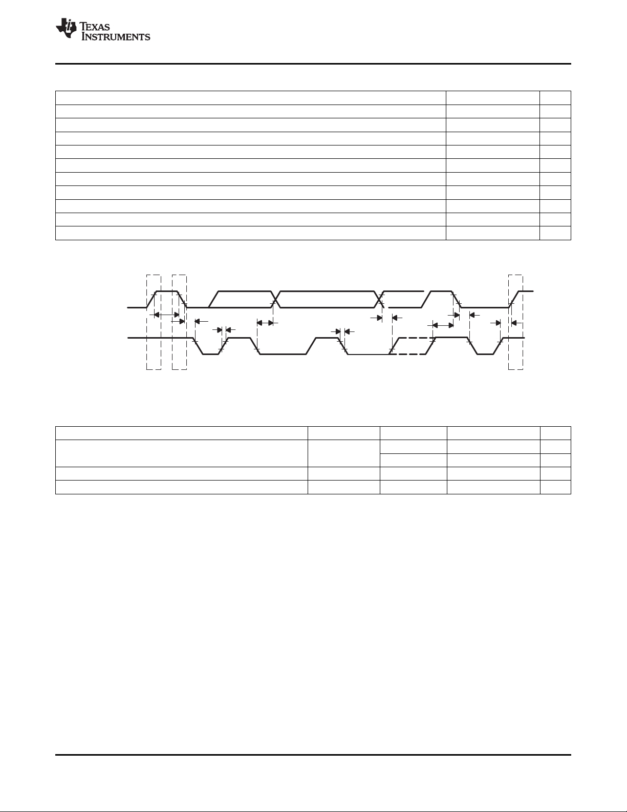
VC1 (SDA)
t
1
t3
t
7
t6
t
8
t5
t2
t3
VC0 (SCL)
Data
Stop Start Stop
t4
TVP5150AM1
www.ti.com
4.8 I2C Host Port Timing
(1)
SLES209D–NOVEMBER 2007–REVISED SEPTEMBER 2010
PARAMETER MIN TYP MAX UNIT
t1 Bus free time between Stop and Start 1.3 µs
t2 Setup time for a (repeated) Start condition 0.6 µs
t3 Hold time (repeated) Start condition 0.6 µs
t4 Setup time for a Stop condition 0.6 ns
t5 Data setup time 100 ns
t6 Data hold time 0 0.9 µs
t7 Rise time, VC1(SDA) and VC0(SCL) signal 250 ns
t8 Fall time, VC1(SDA) and VC0(SCL) signal 250 ns
C
Capacitive load for each bus line 400 pF
b
f
I2C clock frequency 400 kHz
I2C
(1) Specified by design
4.9 Thermal Specifications
PARAMETER PACKAGE BOARD MIN TYP MAX UNIT
q
JA
q
JC
T
J(MAX)
Junction-to-ambient thermal resistance, still air TQFP-32 (PBS)
Junction-to-case thermal resistance, still air TQFP-32 (PBS) 39.3 ºC/W
Maximum junction temperature for reliable operation TQFP-32 (PBS) 105 ºC
Figure 4-2. I2C Host Port Timing
JEDEC Low-K 125.3 ºC/W
JEDEC High-K 91.1 ºC/W
Copyright © 2007–2010, Texas Instruments Incorporated Electrical Specifications 77
Submit Documentation Feedback
Product Folder Link(s): TVP5150AM1

TVP5150AM1
SLES209D–NOVEMBER 2007–REVISED SEPTEMBER 2010
5 Example Register Settings
The following example register settings are provided only as a reference. These settings, given the
assumed input connector, video format, and output format, set up the TVP5150AM1 decoder and provide
video output. Example register settings for other features and the VBI data processor are not provided
here.
5.1 Example 1
5.1.1 Assumptions
Device: TVP5150AM1
Input connector: Composite (AIP1A)
Video format: NTSC-M, PAL (B, G, H, I), or SECAM
NTSC-4.43, PAL-N, and PAL-M are masked from the autoswitch process by default. See the
autoswitch mask register at address 04h.
Output format: 8-bit ITU-R BT.656 with embedded syncs
5.1.2 Recommended Settings
www.ti.com
NOTE
Recommended I2C writes: For this setup, only one write is required. All other registers are set up by
default.
I2C register address 03h = Miscellaneous controls register address
I2C data 09h = Enables YCbCr output and the clock output
NOTE
HSYNC, VSYNC/PALI, AVID, and FID/GLCO are high impedance by default. See the
miscellaneous control register at address 03h.
78 Example Register Settings Copyright © 2007–2010, TexasInstruments Incorporated
Submit Documentation Feedback
Product Folder Link(s): TVP5150AM1

TVP5150AM1
www.ti.com
5.2 Example 2
5.2.1 Assumptions
Device: TVP5150AM1
Input connector: S-video (AIP1A (luminance), AIP1B (chrominance))
Video Format: NTSC (M, 4.43), PAL (B, G, H, I, M, N, Nc) or SECAM (B, D, G, K1, L)
Output format: 8-bit 4:2:2 YCbCr with discrete sync outputs
5.2.2 Recommended Settings
Recommended I2C writes: This setup requires additional writes to output the discrete sync 4:2:2 data
outputs, the HSYNC, and the VSYNC, and to autoswitch between all video formats mentioned above.
I2C register address 00h = Video input source selection #1 register
I2C data 01h = Selects the S-Video input, AIP1A (luminance), and AIP1B (chrominance)
<br/>
I2C register address 03h = Miscellaneous controls register address
I2C data 0Dh = Enables the YCbCr output data, HSYNC, VSYNC/PALI, AVID, and FID/GLCO
<br/>
SLES209D–NOVEMBER 2007–REVISED SEPTEMBER 2010
I2C register address 04h = Autoswitch mask register
I2C data C0h = Unmask NTSC-4.43, PAL-N, and PAL-M from the autoswitch process
<br/>
I2C register address 0Dh = Outputs and data rates select register
I2C data 40h = Enables 8-bit 4:2:2 YCbCr with discrete sync output
Copyright © 2007–2010, Texas Instruments Incorporated Example Register Settings 79
Submit Documentation Feedback
Product Folder Link(s): TVP5150AM1

DVDD
IO_DVDD
IO_DVDD
AVDD
AVID
AVDD
HSYNC
PDN
IO_DVDD
INTERQ/GPCL
PDN
INTREQ/GPCL
AVID
HSYNC
VSYNC/PALI
FID/GLCO
PCLK/SCLK
OSC_IN
YOUT[7:0]
RESETB
VSYNC/PALI
SCL
PCLK/SCLK
CH1_IN
CH2_IN
OSC
SDA
FID/GLCO
C1
1 µF
C5
0.1 µF
R1
R5
C4
0.1 µF
R2
37.4 W
R6
37.4 W
R3
2.2 kW
R4
2.2 kW
C10
0.1 µF
C6
0.1 µF
Y1
14.31818 MHz ± 50 ppm
C2
1 µF
C8
CL1
C3
1 µF
C9
CL2
S1
1 2
C7
0.1 µF
R7
10 kW
TVP5150AM1
1
2
3
4
25526627728829
9
30
10
31
11
32
1213141516
17
18
19
20
21
22
23
24
AIP1A
AIP1B
PLL_AGND
PLL_AVDD
XTAL1/OSC
XTAL2
AGND
RESETB
PCLK/SCLK
IO_DVDD
YOUT7
YOUT6
YOUT5
YOUT4
YOUT3
YOUT2
YOUT1
YOUT0
DGND
DVDD
SCL
SDA
FID/GLCO
VSYNC/PALI
HSYNC
AVID
INTREQ/GPCL/VBLK
PDN
REFP
REFM
CH_AGND
CH_AVDD
Implies I C address is BAh. If B8h is to be used,
connect pulldown resistor to digital ground.
2
0.1 µF
C11
37.4 W
37.4 W
R
AFF
AFF
TVP5150AM1
SLES209D–NOVEMBER 2007–REVISED SEPTEMBER 2010
6 Application Information
6.1 Application Example
www.ti.com
80 Application Information Copyright © 2007–2010, Texas Instruments Incorporated
A. The use of INTREQ/GPCL, AVID, HSYNC, and VSYNC is optional.
B. When OSC is connected through S1, remove the capacitors for the crystal.
C. PDN needs to be high, if device has to be always operational.
D. RESETB is operational only when PDN is high. This allows an active-low reset to the device.
E. 100-kΩ resistor (R) in parallel with the crystal is recommended for most crystal types.
F. Anti-aliasing filter (AAF) highly recommended for best video quality.
Figure 6-1. Application Example
Product Folder Link(s): TVP5150AM1
Submit Documentation Feedback

TVP5150AM1
www.ti.com
7 Revision History
Table 7-1. Revision History
REVISION COMMENTS
SLES209 Initial release
SLES209A AEC-Q100 qualification added
Section 2.3, Related Products added.
Section 2.4, Trademarks modified.
Section 3.16, Figure 3.5, Changed crystal parallel resistor recommendation.
Section 3.21.9, Luminance Brightness description modified.
Section 3.21.10, Chrominance Saturation description modified.
Section 3.21.12, Luminance Contrast description modified.
SLES209B Section 3.21.45, Status Register #3 description modified.
Section 3.21.49, CGMS-A added to register description.
Section 3.21.50, Gemstar 2x added to register description.
Section 3.21.58, Table 3-16, Recommended VBI Configuration RAM settings modifications.
Section 3.21.59, VDP Status Register modifications.
Section 6.1, Changed recommendation for resistor in parallel with the crystal.
Minor editorial changes throughout
Section 3.3, Figure 3-2, Chroma trap filter characteristics for NTSC added.
Section 3.3, Figure 3-3, Chroma trap filter characteristics for PAL added.
SLES209C
SLES209D Section 3.21.31, Added Indirect Register Read/Write Strobe
Section 3.4, Figure 3-4, Color low-pass filter characteristics added.
Section 3.8, Table 3-1, Modified name for register 1100b.
Section 3.20, Table 3-11, Added I2C indirect registers at address 21h-24h.
Section 4.9, Added Power Dissipation Ratings.
Section 3.6, Modified when color killer suppresses chrominance processing.
Section 3.21.29, Added Indirect Register Data
Section 3.21.30, Added Indirect Register Address
Section 3.21.38, Added Patch Write Address
Section 3.21.39, Added Patch Code Execute
Section 3.21.53, Added Patch Read Address
SLES209D–NOVEMBER 2007–REVISED SEPTEMBER 2010
Copyright © 2007–2010, Texas Instruments Incorporated Revision History 81
Submit Documentation Feedback
Product Folder Link(s): TVP5150AM1

IMPORTANT NOTICE
Texas Instruments Incorporated and its subsidiaries (TI) reserve the right to make corrections, modifications, enhancements, improvements,
and other changes to its products and services at any time and to discontinue any product or service without notice. Customers should
obtain the latest relevant information before placing orders and should verify that such information is current and complete. All products are
sold subject to TI’s terms and conditions of sale supplied at the time of order acknowledgment.
TI warrants performance of its hardware products to the specifications applicable at the time of sale in accordance with TI’s standard
warranty. Testing and other quality control techniques are used to the extent TI deems necessary to support this warranty. Except where
mandated by government requirements, testing of all parameters of each product is not necessarily performed.
TI assumes no liability for applications assistance or customer product design. Customers are responsible for their products and
applications using TI components. To minimize the risks associated with customer products and applications, customers should provide
adequate design and operating safeguards.
TI does not warrant or represent that any license, either express or implied, is granted under any TI patent right, copyright, mask work right,
or other TI intellectual property right relating to any combination, machine, or process in which TI products or services are used. Information
published by TI regarding third-party products or services does not constitute a license from TI to use such products or services or a
warranty or endorsement thereof. Use of such information may require a license from a third party under the patents or other intellectual
property of the third party, or a license from TI under the patents or other intellectual property of TI.
Reproduction of TI information in TI data books or data sheets is permissible only if reproduction is without alteration and is accompanied
by all associated warranties, conditions, limitations, and notices. Reproduction of this information with alteration is an unfair and deceptive
business practice. TI is not responsible or liable for such altered documentation. Information of third parties may be subject to additional
restrictions.
Resale of TI products or services with statements different from or beyond the parameters stated by TI for that product or service voids all
express and any implied warranties for the associated TI product or service and is an unfair and deceptive business practice. TI is not
responsible or liable for any such statements.
TI products are not authorized for use in safety-critical applications (such as life support) where a failure of the TI product would reasonably
be expected to cause severe personal injury or death, unless officers of the parties have executed an agreement specifically governing
such use. Buyers represent that they have all necessary expertise in the safety and regulatory ramifications of their applications, and
acknowledge and agree that they are solely responsible for all legal, regulatory and safety-related requirements concerning their products
and any use of TI products in such safety-critical applications, notwithstanding any applications-related information or support that may be
provided by TI. Further, Buyers must fully indemnify TI and its representatives against any damages arising out of the use of TI products in
such safety-critical applications.
TI products are neither designed nor intended for use in military/aerospace applications or environments unless the TI products are
specifically designated by TI as military-grade or "enhanced plastic." Only products designated by TI as military-grade meet military
specifications. Buyers acknowledge and agree that any such use of TI products which TI has not designated as military-grade is solely at
the Buyer's risk, and that they are solely responsible for compliance with all legal and regulatory requirements in connection with such use.
TI products are neither designed nor intended for use in automotive applications or environments unless the specific TI products are
designated by TI as compliant with ISO/TS 16949 requirements. Buyers acknowledge and agree that, if they use any non-designated
products in automotive applications, TI will not be responsible for any failure to meet such requirements.
Following are URLs where you can obtain information on other Texas Instruments products and application solutions:
Products Applications
Amplifiers amplifier.ti.com Audio www.ti.com/audio
Data Converters dataconverter.ti.com Automotive www.ti.com/automotive
DLP® Products www.dlp.com Communications and www.ti.com/communications
DSP dsp.ti.com Computers and www.ti.com/computers
Clocks and Timers www.ti.com/clocks Consumer Electronics www.ti.com/consumer-apps
Interface interface.ti.com Energy www.ti.com/energy
Logic logic.ti.com Industrial www.ti.com/industrial
Power Mgmt power.ti.com Medical www.ti.com/medical
Microcontrollers microcontroller.ti.com Security www.ti.com/security
RFID www.ti-rfid.com Space, Avionics & www.ti.com/space-avionics-defense
RF/IF and ZigBee® Solutions www.ti.com/lprf Video and Imaging www.ti.com/video
Mailing Address: Texas Instruments, Post Office Box 655303, Dallas, Texas 75265
Copyright © 2010, Texas Instruments Incorporated
Telecom
Peripherals
Defense
Wireless www.ti.com/wireless-apps
 Loading...