

Texas Instruments TVP3703-170CFN, TVP3703-135CFN Datasheet

TVP3703
VIDEO INTERFACE PALETTE
TRUE-COLOR CMOS RAMDAC
SLAS100 – MARCH 1996
Copyright 1996, Texas Instruments Incorporated
1
POST OFFICE BOX 655303 • DALLAS, TEXAS 75265
• Fully Integrated Dual Clock Synthesizer
and 16-Bit Pixel Port True-Color RAMDAC
• Two Phase-Locked-Loop (PLL)
Synthesizers Provide Independently
Controlled Video and Memory Clock
Outputs
• Functionally Interchangeable with STG1703
• On-Chip PLL Clock Reference Requires
Single External Crystal
• 16-Bit Pixel Port Supports VGA High-Color
and True-Color Standards Up to 170 MHz
• Programmable Power-Down Features
• On-Chip Cyclic Redundancy Check (CRC)
Test
description
The TVP3703 is a super video graphics array (SVGA) compatible, true-color CMOS RAMDAC with integrated
clock synthesizers that can provide the memory and pixel clock signals for a PC graphics subsystem. The video
clock can be one of two VGA base frequencies or fourteen Video Electronics Standards Association (VESA)
standard frequencies which can also be reprogrammed through the standard micro port interface.
The memory clock output is also user programmable at frequencies up to 80 MHz. The pixel modes supported
by the TVP3703 include:
• Serializing 16-bit pixel port providing 170 MHz, 8-bit and 73 MHz, 24-bit packed pixel modes using an
internal PLL
• 16-bit pixel port providing faster, high-color/true-color operation up to the 110 MHz sampling rate
• 8-bit pixel port providing standard SVGA and high-color/true-color modes up to the 1 10 MHz sampling rate
The 68 terminal FN package is designed to be interchangeable with the STG1703.
28 29
GND
P7
P6
P5
P4
P3
P2
P1
P0
REF
RS2
COMP
RSET
VS3
VS2
VS1
VS0
60
59
58
57
56
55
54
53
52
51
50
49
48
47
46
45
44
30
10
11
12
13
14
15
16
17
18
19
20
21
22
23
24
25
26
GND
BLANK
D0
D1
D2
D3
D4
D5
D6
D7
WR
RS0
RS1
P14
PIXMIX
P15
NC
31 32 33 34
FN PACKAGE
(TOP VIEW)
SENSE
P1 1
87 65493
XIN
XOUTRDP13
GND
P12
GND
GND
RED
GREEN
NCNCNCNCNC
NC
168672
35 36 37 38 39
66 65
27
NC
P10
P9
64 63 62 61
40 41 42 43
BLUE
GND
STROBE
P8
PCLK
MCLK
VCLK
DD
V
DD
VA
DD
V
DD
V
DD
V
DD
VA
NC – No internal connection
PRODUCTION DATA information is current as of publication date.
Products conform to specifications per the terms of Texas Instruments
standard warranty. Production processing does not necessarily include
testing of all parameters.

TVP3703
VIDEO INTERFACE PALETTE
TRUE-COLOR CMOS RAMDAC
SLAS100 – MARCH 1996
2
POST OFFICE BOX 655303 • DALLAS, TEXAS 75265
applications
• Screen resolutions (noninterlaced)
– 1600 × 1280, 8-bit/pixel, 60 Hz
– 1280 × 1024, 16-bit/pixel, 60 Hz
– 1024 × 768, 16-bit/pixel, 85 Hz
– 1024 × 768, 24-bit/pixel, packed, 70 Hz
– 800 × 600, 24-bit/pixel, unpacked, 72 Hz
• True-color desktop, PC add-in cards
functional block diagram
Multiplexor Mask
256×8 Bit
Color Palette
256×8 Bit
Color Palette
256×8 Bit
Color Palette
Bypass Multiplexor
24
DAC
DAC
DAC
DAC
Comparators
DAC
Control
RED
BLUE
Micro Port
MCLK
PLL
MCLK
Registers
Crystal
Oscillator
VCLK
PLL
VCLK
Registers
Internal
REF
Pipeline
Timing
Pixel
Latches
3
D0–D7
RD
WR
RS0-RS2
VS0-VS3
STROBE
PIXMIX
P0–P15
PCLK
REF
RSET
BLANK
COMP SENSE
MCLK XIN XOUT VCLK
GREEN

TVP3703
VIDEO INTERFACE PALETTE
TRUE-COLOR CMOS RAMDAC
SLAS100 – MARCH 1996
3
POST OFFICE BOX 655303 • DALLAS, TEXAS 75265
Terminal Functions
micro port
TERMINAL
NAME NO.
I/O
DESCRIPTION
RD,
5, I
Read enable and write enable. RD or WR control the timing of read and write operations on the micro port.
WR
20
Most of the operations on the micro port can take place asynchronously to the pixel stream being processed
by the color palette. Various minimum periods between operations are specified (in terms of pixel clocks) to
allow this asynchronous behavior.
RD and WR should not be low at the same time.
RS0–RS2 21, 22,50I
Register select. RS0–RS2 specify which internal register is to be accessed. The RS0–RS2 inputs are sampled
on the falling edge of the active enable signal (RD
or WR). Information on register access and contents is given
in the micro port section.
The additional RS2 signal allows access to the extended features without the need for performing an indirect
access sequence.
D0–D7 12–19 I/O
Input/output data. Data transfers between the 8-bit wide program data bus and the registers within the TVP3703
under control of the active enable signal (RD
or WR).
In a write cycle, the rising edge of WR validates the data on the program data bus and causes it to be written
to the register selected.
The rising edge of RD signifies the end of a read cycle, after which the program data bus ceases to carry the
contents of the register addressed and goes to a high impedance state.
VS0–VS3 44–47 I Video clock PLL select.VS0–VS3 select the frequency (default or user programmed) of the video clock PLL.
VS0–VS3 are ignored if the video clock frequency is selected by register control.
STROBE 43 I Strobe input.The falling edge of STROBE latches VS0–VS3.
pixel port
TERMINAL
NAME NO.
I/O
DESCRIPTION
PCLK 63 I Pixel clock. The rising edge of PCLK controls the sampling of data on P0–P15, BLANK, and PIXMIX in all
modes.
P0 –P15 1, 4, 23,
25,
52–59,
64–67
I Pixel data word. The selected pixel mode determines how this pixel data is interpreted.
PIXMIX 24 I Pixel mode select. PIXMIX controls the switching between primary and secondary pixel modes when the
extended pixel modes are selected (PIXMIX = 0 selects primary mode).
BLANK 11 I Blank in. A low value sampled on BLANK, after the pipeline delay , turns the DAC outputs off.
TVP3703
VIDEO INTERFACE PALETTE
TRUE-COLOR CMOS RAMDAC
SLAS100 – MARCH 1996
4
POST OFFICE BOX 655303 • DALLAS, TEXAS 75265
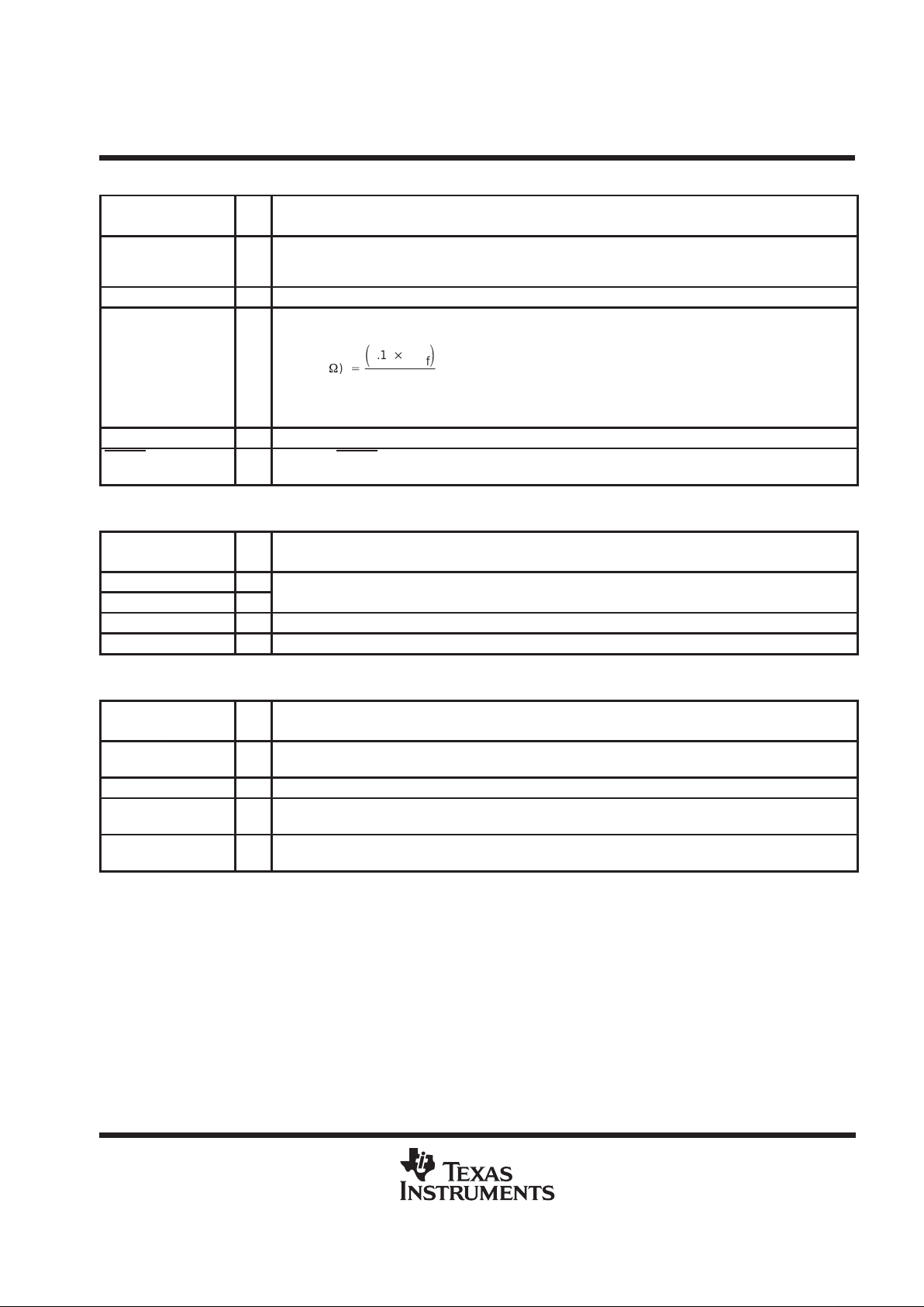
DAC interface
TERMINAL
NAME NO.
I/O
DESCRIPTION
RED,
GREEN,
BLUE
38–40 O DAC video outputs. These signals are designed to drive a doubly terminated 75-Ω load.
REF 51 I External 1.235-V reference voltage. An external bypass capacitor should be connected from REF to GND.
RSET 48 I A precision resistor placed between RSET and GND sets the full-scale DAC current. The required resistor value
can be calculated from:
where V
ref
is the external or internal reference voltage and IO is the required DAC full-scale output current. R
set
is typically 147 Ω for VGA (see application information section).
COMP 49 I External compensation capacitor connection for DACs.
SENSE 68 O Sense out. SENSE is a logical 0 if one or more of the DAC outputs exceeds the internal DAC comparator trip
voltage (which is midway between the DAC full scale and GND potentials).
frequency synthesizer interface
TERMINAL
NAME NO.
I/O
DESCRIPTION
XOUT 6 O
Crystal output and input connections. A series-resonant crystal must be connected between XOUT and XIN
XIN 7 I
to provide the reference clock for the PLLs.
VCLK 9 O Video clock PLL out
MCLK 61 O Memory clock PLL out
power supply
TERMINAL
NAME NO.
I/O
DESCRIPTION
V
DD
8, 27, 35,
62
Digital power
AV
DD
3, 42 Analog power for the DACs and PLL.
GND 2, 10, 36,
37, 41, 60
Common ground rail for all circuitry.
NC 26, 28–34 No internal connection. For future upgrade to a 24-bit pixel port the controller. Outputs P16–P23 can be routed
to terminals 26, 28–34 respectively.
detailed description
micro port
The TVP3703 micro port (see Table 1) is an extension of the standard VGA micro port and powers up with a
register configuration compatible with standard and high-color VGA. There are two methods for accessing the
register set of the TVP3703 – direct register space (RS) access and indirect access.
direct RS access
This feature supports direct RS mapping to eight address locations that access the VGA color palette, pixel
command register, and an indexed register. The index low/high registers increment after every access to the
indexed register.
R
set
(W)
+
ǒ
2.1 V
ref
Ǔ
I
O
TVP3703
VIDEO INTERFACE PALETTE
TRUE-COLOR CMOS RAMDAC
SLAS100 – MARCH 1996
5
POST OFFICE BOX 655303 • DALLAS, TEXAS 75265
direct RS access (continued)
T able 1. Direct RS Micro Port Accesses
RS(2–0) VGA REGISTER
000 Address register (palette write)
001 Palette color value
010 Pixel mask/indirect access
011 Address register (palette read)
100 Index low byte
101 Indexed register
110 Pixel command register
111 Index high byte
indirect access
The indexed register space can also be accessed by a special mechanism of successive reads to the mask
register location 2h, as shown in Table 2. Reads from RS location 2h cause a state counter to be advanced by
one. Five successive reads of RS location 2h returns the mask register contents four times followed by the pixel
command register value.
If the indexed register space is not enabled, the next access is directed to the pixel mask (state 1 in Table 2).
States 3 to 4 require three reads from the pixel mask register and, when the pixel command register is written
to enable the indexed register space, the next access is again directed to the mask register (the next state after
state 5 is state 1).
The indirect access sequence can now enter states 6 and 7 to access the lower and higher byte of the index
register respectively . Subsequent reads or writes to location 2h access the register space pointed to by the index
register. After each indexed register access, the index register increments automatically. In this way, the entire
indexed register space can be moved as a block without the need to keep writing to the index register.
At any point in the above sequence, a read or write to any location other than 2h resets the state counter to
state 1.
On power up, the indirect access is truncated through the default setting of pixel command register bit 4 so that
the TVP3703 is identified by existing video basic input/output system (BIOS) code as a fast ATT20C490
RAMDAC.
Table 2. Indirect Access Sequence
CURRENT STATE
†
NEXT STATE
STATE
REGISTER MAPPED
AT RS = 2h
READ FROM
RS = 2h AND INDEX
SPACE ENABLED
READ FROM
RS = 2h AND INDEX
SPACE DISABLED
(DEFAULT)
WRITE TO
RS = 2h
READ/WRITE TO
OTHER RS LOCATION
1 Pixel mask 2 2 1 1
2 Pixel mask 3 3 1 1
3 Pixel mask 4 4 1 1
4 Pixel mask 5 5 1 1
5 Pixel command 6 1 1 1
6 Index low byte 7 7 1
7 Index high byte 8 8 1
8 Indexed register 8
‡
8
‡
1
†
Power-up state is state 1.
‡
Increment index register after access

TVP3703
VIDEO INTERFACE PALETTE
TRUE-COLOR CMOS RAMDAC
SLAS100 – MARCH 1996
6
POST OFFICE BOX 655303 • DALLAS, TEXAS 75265
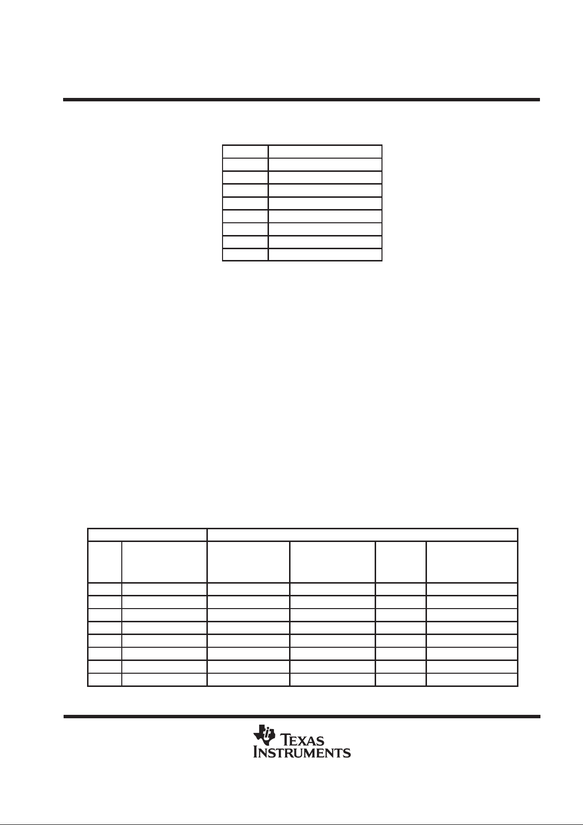
indexed register space
The TVP3703 indexed register space including the indexes, register contents, and values is shown in Table 3.
Table 3. Indexed Register Space
INDEX INDEX REGISTER CONTENTS
†
VALUE
‡
00 00h Company ID = 97h
00 01h Device ID = 03h
00 02h Reserved (see Note 1)
00 03h Primary pixel mode select
00 04h Secondary pixel mode select
00 05h Pipeline timing control
00 06h Soft reset
00 07h Power management A
00 08h Power management B
00 09h –
00 1Fh
Reserved (see Note 1)
00 20h VCLK V0 parameters low (3Dh)
00 21h VCLK V0 parameters high (47h)
25.175
00 22h VCLK V1 parameters low (55h)
00 23h VCLK V1 parameters high (49h)
28.332
00 24h VCLK V2 parameters low (41h)
00 25h VCLK V2 parameters high (2Ah)
40.0
00 26h VCLK V3 parameters low (26h)
00 27h VCLK V3 parameters high (06h)
72.0
00 28h VCLK V4 parameters low (36h)
00 29h VCLK V4 parameters high (26h)
50.0
00 2Ah VCLK V5 parameters low (29h)
00 2Bh VCLK V5 parameters high (06h)
77.0
00 2Ch VCLK V6 parameters low (26h)
00 2Dh VCLK V6 parameters high (26h)
36.0
00 2Eh VCLK V7 parameters low (43h)
00 2Fh VCLK V7 parameters high (29h)
44.90
00 30h VCLK V8 parameters low (59h)
00 31h VCLK V8 parameters high (08h)
130.00
00 32h VCLK V9 parameters low (41h)
00 33h VCLK V9 parameters high (06h)
120.00
INDEX INDEX REGISTER CONTENTS
†
VALUE
‡
00 34h VCLK V10 parameters low (41h)
00 35h VCLK V10 parameters high (0Ah)
80.0
00 36h VCLK V11 parameters low (56h)
00 37h VCLK V11 parameters high (48h)
31.50
00 38h VCLK V12 parameters low (43h)
00 39h VCLK V12 parameters high (07h)
110.0
00 3Ah VCLK V13 parameters low (59h)
00 3Bh VCLK V13 parameters high (28h)
65.0
00 3Ch VCLK V14 parameters low (28h)
00 3Dh VCLK V14 parameters high (06h)
75.0
00 3Eh VCLK V15 parameters low (40h)
00 3Fh VCLK V15 parameters high (08h)
94.50
00 40h MCLK M0 parameters low (3Dh)
00 41h MCLK M0 parameters high (28h)
45.0
00 42h MCLK M1 parameters low (51h)
00 43h MCLK M1 parameters high (27h)
66.0
00 44h MCLK M2 parameters low (2Ah)
00 45h MCLK M2 parameters high (07h)
70.0
00 46h MCLK M3 parameters low (36h)
00 47h MCLK M3 parameters high (08h)
80.0
00 48h Clock synthesizer control (00h)
00 49h –
FF D5h
Reserved (see Note 1)
FF D6h CRC Test
FF D7h CRC low byte
FF D8h CRC high byte
FF D9h
Red, green, blue (RGB) DAC input
data test
FF DAh –
FF FFh
Reserved (see Note 1)
†
Register power-up values for given synthesizer frequencies are shown in parentheses.
‡
Synthesizer frequencies given for f
I(XIN)
= 14.31818 MHz
NOTE 1: Do not write to reserved locations

TVP3703
VIDEO INTERFACE PALETTE
TRUE-COLOR CMOS RAMDAC
SLAS100 – MARCH 1996
7
POST OFFICE BOX 655303 • DALLAS, TEXAS 75265
register content descriptions
A write to any register containing reserved bits should always write 0s to the reserved bits (the exception being
bit 7 of power management register A). On reads, all reserved bits should be masked out.
The values of register bits that are reset on power-up are listed in the reset value columns below.
PIXEL COMMAND REGISTER (RS0–RS2 = 110)
BIT VALUE FUNCTION
RESET
VALUE
000 8-bit color
001 Reserved
010 Reserved
011 Reserved
7–5
100 Reserved
000
101 15-bit direct color
110 16-bit direct color
111 24-bit direct color
4 1 = Enable extended register space 0
3 1 = Enable extended pixel modes 0
2 1 = Add 7.5 IRE† blanking pedestal 0
1
1 = Micro port interface to RAM is
8-bit not 6-bit
0
0
1 = Sleep mode (micro port and
palette RAM still enabled, see power
management features section)
0
†
Institute of Radio Engineers
INDEX LOW AND HIGH BYTE REGISTERS
(RS0–RS2 = 100, RS0–RS2 = 111)
BIT FUNCTION
RESET
VALUE
7–0 Low/high byte of 16-bit index 0
COMPANY ID REGISTER (Index 0000h)
BIT VALUE FUNCTION
RESET
VALUE
7–0 97h T exas Instruments Read only
DEVICE ID REGISTER (Index 0001h)
BIT VALUE FUNCTION
RESET
VALUE
7–0 03h TVP3703 Read only
PIXEL MODE SELECT REGISTERS
(Primary and Secondary) (Indexes 0003h, 0004h)
BIT VALUE FUNCTION
MAX
PCLK
(MHz)
MAX
VIDEO
RATE
(MHz)
RESET
VALUE
00h 8-bit indexed color 110 110
01h
15-bit direct color or
8-bit indexed color
110 110
02h 15-bit direct color 110 110
03h
16-bit 5–6–5 direct
color
110 110
04h 24-bit direct color 110 55
05h
Double 8-bit indexed
color
67.5 135
7–0
06h
16-bit 5–6–5 direct
color (2 × 8-bit input)
110 55
Not
Reset
07h
8-bit indexed color
(2 × 4-bit input)
110 55
08h
15-bit direct color
(2 × 4-bit input)
110 55
09h
Double 24-bit direct
color
85 56.5
0Ah–
FFh
Reserved
PIPELINE TIMING CONTROL REGISTER
(Double 8-bit and 24-bit modes only)
(Index 0005h)
The TVP3703 uses an internal PLL and timing control circuitry to
automatically adjust pipeline. There are no register bits to program,
since the device accounts for all desired frequency ranges.
SOFT RESET REGISTER (Index 0006h)
BIT FUNCTION
RESET
VALUE
7–1 Reserved 0
0 1 = Reset all registers to power-on default state 0
 Loading...