

TEXAS INSTRUMENTS TUSB2043 Technical data
D
Universal Serial Bus (USB) Version 1.1
Compliant
D
32-Pin TQFP Package With a 0.8 mm Pin
Pitch
D
3.3-V Low Power ASIC Logic
D
Integrated USB Transceivers
D
State Machine Implementation Requires No
Firmware Programming
D
One Upstream Port and Four Downstream
Ports
D
All Downstream Ports Support Full-Speed
and Low-Speed Operations
D
Two Power Source Modes
– Self-Powered Mode
– Bus-Powered Mode
D
Power Switching and Over-Current
Reporting is Provided Ganged or Per Port
D
Supports Suspend and Resume Operations
D
Supports Programmable Vendor ID and
Product ID With External Serial EEPROM
D
3-State EEPROM Interface Allows EEPROM
Sharing
D
Push-Pull Outputs for PWRON Eliminate
the Need for External Pullup Resistors
D
Noise Filtering on OVRCUR Provides
Immunity to Voltage Spikes
D
Package Pinout Allows 2-Layer PCB
D
Migrated From Proven TUSB2040 Hub
D
Lower Cost Than the TUSB2040 Hub
description
TUSB2043
4-PORT HUB FOR THE UNIVERSAL SERIAL BUS
WITH OPTIONAL SERIAL EEPROM INTERFACE
SLLS308A – FEBRUARY 1999 – REVISED AUGUST 1999
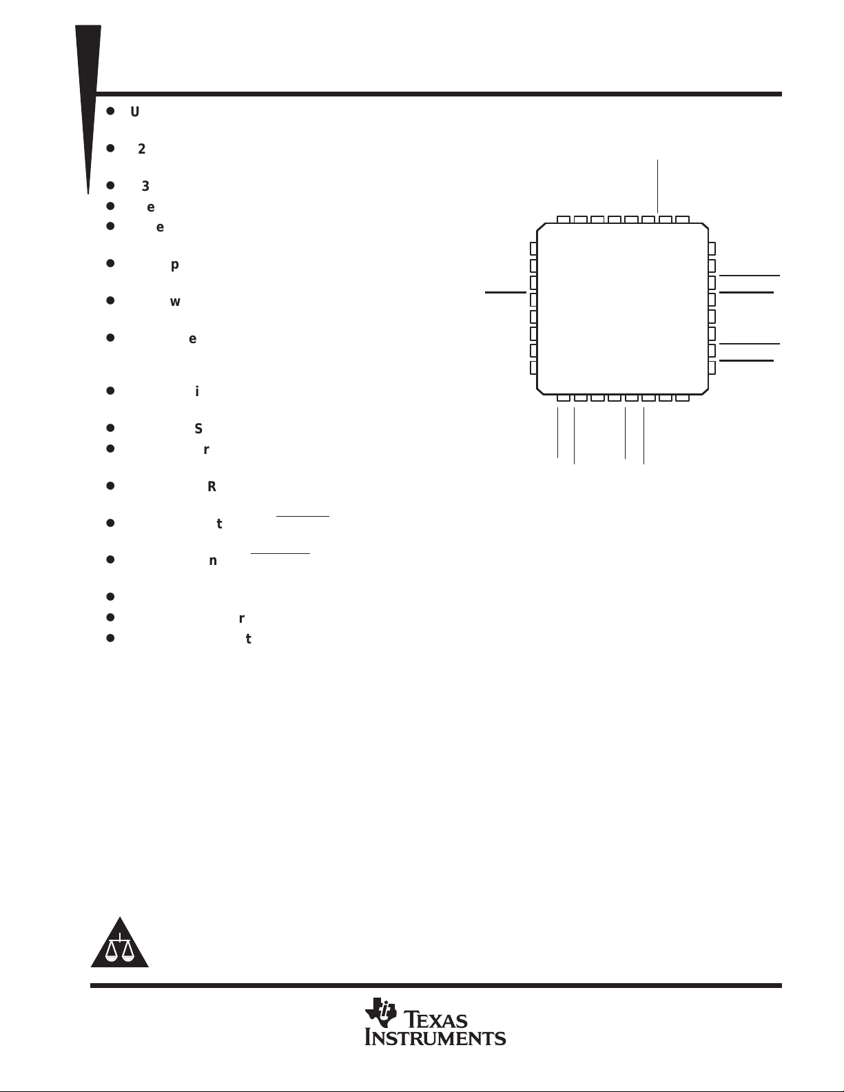
VF PACKAGE
(TOP VIEW)
CC
V
CLKIN
EXTMEM
25
24
23
22
21
20
19
18
17
16
DP2
DM2
OVRCUR2
DP4
DM4
OVRCUR4
PWRON4
DP3
DM3
OVRCUR3
PWRON3
DP0
DM0
V
CC
RESET
EECLK
EEDATA/GANGED
GND
BUSPWR
SUSPND
MODESLCT
TESTIN
TESTOUT
32 26
31 30 29 28 27
1
2
3
4
5
6
7
8
11 12 13 14 15
910
DP1
DM1
PWRON1
OVRCUR1
GND
PWRON2
The TUSB2043 is a 3.3 V CMOS hub device that provides one upstream port and four downstream ports in
compliance with the 1.1 Universal Serial Bus (USB) specification. Because this device is implemented with a
digital state machine instead of a microcontroller, no firmware programming is required. Fully compliant USB
transceivers are integrated into the ASIC for all upstream and downstream ports. The downstream ports support
both full-speed and low-speed devices by automatically setting the slew rate according to the speed of the
device attached to the ports. The configuration of the BUSPWR pin selects either the bus-powered or the
self-powered mode.
Please be aware that an important notice concerning availability, standard warranty, and use in critical applications of
Texas Instruments semiconductor products and disclaimers thereto appears at the end of this data sheet.
PRODUCTION DATA information is current as of publication date.
Products conform to specifications per the terms of Texas Instruments
standard warranty. Production processing does not necessarily include
testing of all parameters.
POST OFFICE BOX 655303 • DALLAS, TEXAS 75265
Copyright 1999, Texas Instruments Incorporated
1

TUSB2043
4-PORT HUB FOR THE UNIVERSAL SERIAL BUS
WITH OPTIONAL SERIAL EEPROM INTERFACE
SLLS308A – FEBRUARY 1999 – REVISED AUGUST 1999
description (continued)
Configuring the GANGED input determines the power switching and over-current detection modes for the
downstream ports. External power management devices such as the TPS2044 are required to control the 5-V
source to the downstream ports according to the corresponding values of the PWRON pin. Upon detecting any
over-current conditions, the power management device sets the corresponding OVRCUR
to a logic low. If GANGED is high, all PWRON outputs switch together and if any OVRCUR is activated, all ports
transition to power-off state. If GANGED is low , the PWRON outputs and OVRCUR inputs operate on a per port
basis.
The EXTMEM pin enables or disables the optional EEPROM interface. When the EXTMEM pin is high, the
product ID (PID) displayed during enumeration is General-Purpose USB Hub. For this default, pin 5 is disabled
and pin 6 functions as the GANGED input pin. If custom PID and Vendor ID (VID) descriptors are desired, the
EXTMEM
interface with pin 5 and pin 6 functioning as the EECLK and EEDA TA, respectively . See Table 1 for a description
of the EEPROM memory map.
Other useful features of the TUSB2043 include a package with a 0.8 mm pin pitch for easy PCB routing and
assembly , push-pull outputs for the PWRON pins eliminate the need for pullup resistors required by traditional
open collector I/Os, and OVRCUR pins with noise filtering for increased immunity to voltage spikes.
pin must be low (EXTMEM = 0). For this configuration, pin 5 and pin 6 function as the EEPROM
pin of the TUSB2043
2
POST OFFICE BOX 655303 • DALLAS, TEXAS 75265
functional block diagram
Hub Repeater
DP0 DM0
12
USB
Transceiver
Suspend/Resume
Logic and
Frame Timer
TUSB2043
4-PORT HUB FOR THE UNIVERSAL SERIAL BUS
WITH OPTIONAL SERIAL EEPROM INTERFACE
SLLS308A – FEBRUARY 1999 – REVISED AUGUST 1999
32
SUSPND
27
CLKIN
30
TESTIN
29
TESTOUT
31
MODESLCT
4
RESET
26
EXTMEM
6
EEDATA/GANGED
5
EECLK
SIE Interface
Logic
Mode
Control
Logic
SIE
Serial
EEPROM
Interface
Port 4
Logic
USB
Transceiver
24 23
DP4 DM4
Port 3
Logic
USB
Transceiver
20 19
Port 2
Logic
USB
Transceiver
16 15
DP2 DM2DP3 DM3
Port 1
Logic
Transceiver
12 11
USB
DP1 DM1
Hub/Device
Command
Decoder
Hub
Power
Logic
10, 14, 18, 22
9, 13, 17, 21
8
BUSPWR
OVRCUR1 – OVRCUR4
PWRON1 – PWRON4
POST OFFICE BOX 655303 • DALLAS, TEXAS 75265
3
TUSB2043
I/O
DESCRIPTION
4-PORT HUB FOR THE UNIVERSAL SERIAL BUS
WITH OPTIONAL SERIAL EEPROM INTERFACE
SLLS308A – FEBRUARY 1999 – REVISED AUGUST 1999
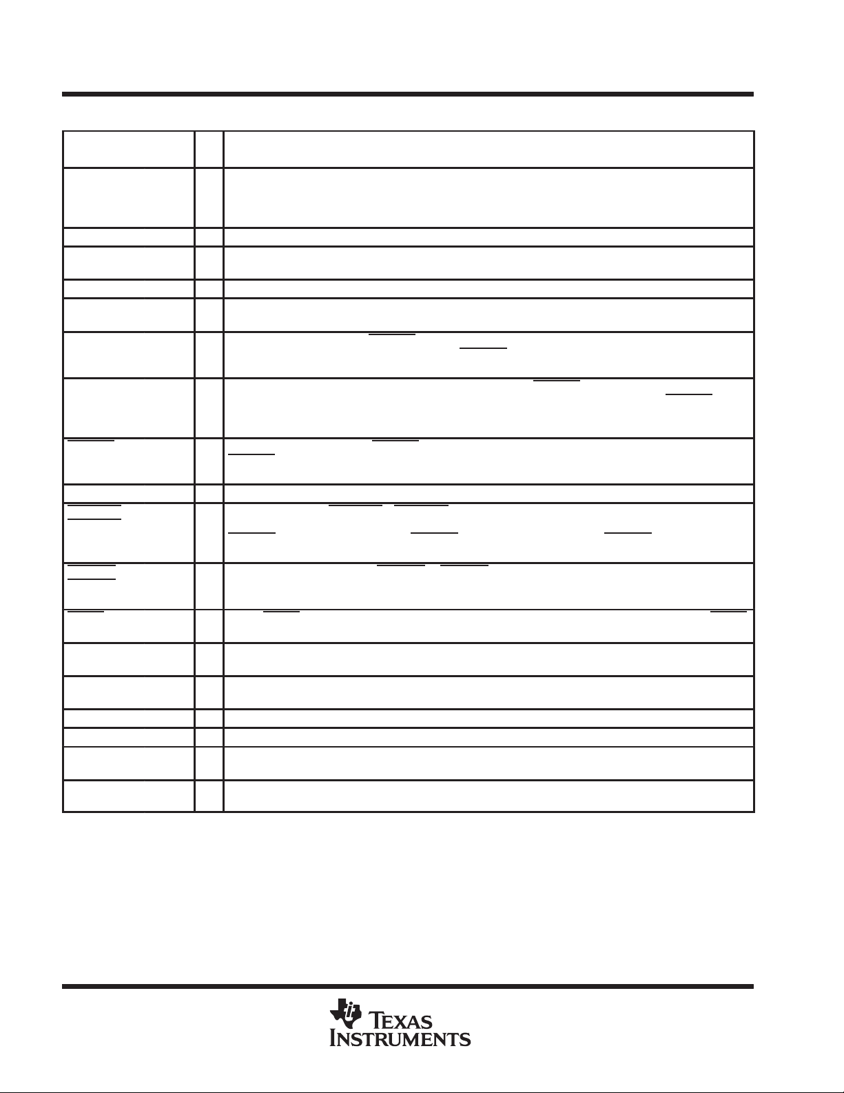
Terminal Functions
TERMINAL
NAME NO.
BUSPWR 8 I Power source indicator. BUSPWR is an active high input that indicates whether the downstream ports source
DM0 2 I/O Root port USB differential data minus. DM0 paired with DP0 constitutes the upstream USB port.
DM1 – DM4 11, 15,
DP0 1 I/O Root port USB differential data plus. DP0 paired with DM0 constitutes the upstream USB port.
DP1 – DP4 12, 16,
EECLK 5 O EEPROM serial clock. When EXTMEM is high, the EEPROM interace is disabled. The EECLK pin is disabled
EEDATA/
GANGED
EXTMEM 26 I EEPROM read enable. When EXTMEM is high, the serial EEPROM interface of the device is disabled. When
GND 7, 28 Ground. GND terminals must be tied to ground for proper operation.
OVRCUR1 –
OVRCUR4
PWRON1 –
PWRON4
RESET 4 I Reset. RESET is an active low TTL input with hysteresis and must be asserted at power up. When RESET
SUSPND 32 O Suspend status. SUSPND is an active high output available for external logic power down operations. During
MODESLCT 31 I Mode select pin. With a simple RC circuit, this pin ensures the normal operation mode is selected. Refer to
CLKIN 27 I 48 MHz clock input. Tie this pin to the output of the oscillator.
V
CC
TESTIN 30 I Test input pin. This pin is used as a test input pin during production test. TESTIN must be tied to VCC (3.3 V)
TESTOUT 29 O T est output pin. This pin is used as a test output pin during production test. TESTOUT must be left open during
19, 23
20, 24
6 I/O EEPROM serial data/power management mode indicator. When EXTMEM is high, EEDA T A/GANGED selects
10, 14,
18, 22
9, 13,
17, 21
3, 25 3.3-V supply voltage
their power from the USB cable or a local power supply. For the bus-power mode, this pin should be pulled
to 3.3 V, and for the self-powered mode, this pin should be pulled low . This standard TTL input must not change
dynamically during operation.
I/O USB differential data minus. DM1 – DM4 paired with DP1 – DP4 support up to four downstream USB ports.
I/O USB differential data plus. DP1 – DP4 paired with DM1 – DM4 support up to four downstream USB ports.
and should be left floating (unconnected). When EXTMEM
to the EEPROM with a 100 µA internal pulldown.
between gang or per-port power over-current detection for the downstream ports. When EXTMEM
EEDATA/GANGED acts as a serial data I/O for the EEPROM and is internally pulled down with a 100 µA
pulldown. This standard TTL input must not change dynamically during operation.
EXTMEM
respectively.
I Over-current inputs. OVRCUR1 – OVRCUR4 are active low, standard TTL inputs. For per-port over current
detection, one over-current input is available for each of the four downstream ports. In the ganged mode, any
OVRCUR
inputs with noise filtering logic.
O Power-on/-off control signals. PWRON1 – PWRON4 are active low, push-pull outputs. Push-pull outputs
eliminate the pullup resistors which open-drain outputs require. However, the external power switches that
connect to these pins must be able to operate with 3.3 V inputs because these outputs cannot drive 5 V signals.
is asserted, all logic is initialized.
the suspend mode, SUSPND is high. SUSPND is low for normal operation.
application information section for detailed information.
for normal operation.
normal operation.
is low, terminals 5 and 6 are configured as the clock and data pins of the serial EEPROM interface,
input may be used and all OVRCUR pins should be tied together. OVRCUR pins are active low
is low, EECLK acts as a 3-state serial clock output
is low,
4
POST OFFICE BOX 655303 • DALLAS, TEXAS 75265
TUSB2043
4-PORT HUB FOR THE UNIVERSAL SERIAL BUS
WITH OPTIONAL SERIAL EEPROM INTERFACE
SLLS308A – FEBRUARY 1999 – REVISED AUGUST 1999
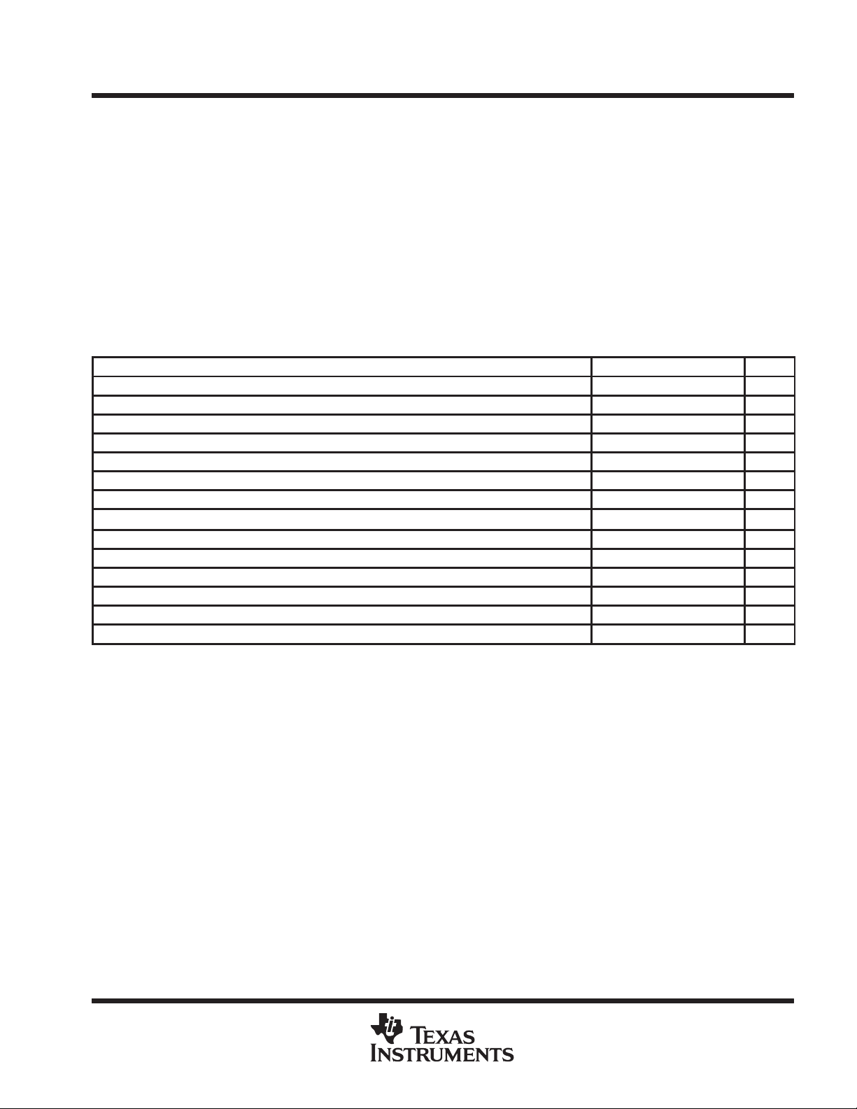
absolute maximum ratings over operating free-air temperature range (unless otherwise noted)
Supply voltage range, VCC (see Note 1) –0.5 V to 3.6 V. . . . . . . . . . . . . . . . . . . . . . . . . . . . . . . . . . . . . . . . . . . . .
Input voltage range, VI –0.5 V to VCC + 0.5 V. . . . . . . . . . . . . . . . . . . . . . . . . . . . . . . . . . . . . . . . . . . . . . . . . . . . . .
Output voltage range, V
–0.5 V to VCC + 0.5 V. . . . . . . . . . . . . . . . . . . . . . . . . . . . . . . . . . . . . . . . . . . . . . . . . . . .
O
Input clamp current, IIK, (VI < 0 V or VI > VCC) ±20 mA. . . . . . . . . . . . . . . . . . . . . . . . . . . . . . . . . . . . . . . . . . . . .
Output clamp current, IOK, (VO < 0 V or V
Storage temperature range, T
–65°C to 150°C. . . . . . . . . . . . . . . . . . . . . . . . . . . . . . . . . . . . . . . . . . . . . . . . . . .
stg
> VCC) ±20 mA. . . . . . . . . . . . . . . . . . . . . . . . . . . . . . . . . . . . . . . . .
O
Operating free-air temperature range, TA 0°C to 70°C. . . . . . . . . . . . . . . . . . . . . . . . . . . . . . . . . . . . . . . . . . . . . .
†
Stresses beyond those listed under “absolute maximum ratings” may cause permanent damage to the device. These are stress ratings only, and
functional operation of the device at these or any other conditions beyond those indicated under “recommended operating conditions” is not
implied. Exposure to absolute-maximum-rated conditions for extended periods may affect device reliability.
NOTE 1: All voltage levels are with respect to GND.
recommended operating conditions
MIN NOM MAX UNIT
Supply voltage, V
Input voltage, TTL/LVCMOS, V
Output voltage, TTL/LVCMOS, V
High-level input voltage, signal-ended receiver, V
Low-level input voltage, signal-ended receiver, V
High-level input voltage, TTL/LVCMOS, V
Low-level input voltage, TTL/LVCMOS, V
Operating free-air temperature, T
External series, differential driver resistor, R
Operating (dc differential driver) high speed mode, f
Operating (dc differential driver) low speed mode, f
Common mode, input range, differential receiver , V
Input transition times, tt, TTL/LVCMOS 0 25 ns
Junction temperature range, T
CC
I
O
IH(REC)
IL(REC)
IH(TTL)
IL(TTL)
A
(DRV)
(OPRH)
(OPRL)
(ICR)
J
3 3.3 3.6 V
0 V
0 V
2 V
2 V
0 0.8 V
0 70 °C
22 (–5%) 22 (5%) Ω
0.8 2.5 V
0 115 °C
CC
CC
CC
0.8 V
CC
12 Mb/s
1.5 Mb/s
V
V
V
V
†
POST OFFICE BOX 655303 • DALLAS, TEXAS 75265
5
 Loading...