

TSB14C01A, TSB14C01AI, TSB14C01AM
5-V IEEE 1394-1995 BACKPLANE TRANSCEIVER/ARBITER
SGLS107A – FEBRUARY 1999 – REVISED NOVEMBER 1999
D
Supports Provisions of IEEE 1394-1995
(1394) Standard for High-Performance
Serial Bus
D
Fully Interoperable With FireWire
†
Implementation of 1394
D
Provides A Backplane Environment That
Supports 50 or 100 Megabits per Second
(Mbits/s)
D
Logic Performs System Initialization and
Arbitration Functions
D
Encode and Decode Functions Included for
Data-Strobe Bit-Level Encoding
D
Incoming Data Resynchronized to Local
Clock
description
The TSB14C01A provides the transceiver functions needed to implement a single port node in a backplanebased 1394 network. The TSB14C01A provides two terminals for transmitting, two terminals for receiving, and
a single terminal to externally control the drivers for data and strobe. The TSB14C01A is not designed to drive
the backplane directly , this function must be provided externally . The TSB14C01A is designed to interface with
a link-layer controller (link), such as the TSB12C01A.
D
Separate Transmitter and Receiver for
Greater Flexibility
D
Data Interface to Link-Layer Controller
(Link) Provided Through Two Parallel
Signal Lines at 25/50 MHz
D
100-MHz or 50-MHz Oscillator Provides
Transmit, Receive-Data, and Link Clocks at
25/50 MHz
D
Single 5-V Supply Operation
D
Packaged in a High-Performance 64-Pin
TQFP (PM) Package for 0°C to 70°C
Operation and –40°C to 85°C Operation
D
Packaged in a 68-Pin CFP (HV) Package for
–55°C to 125°C Operation
The TSB14C01A requires an external 98.304-MHz or 49.152-MHz reference oscillator input for S100/50
operation. The reference signal is internally divided to provide the 49.152-MHz ±100-ppm system clock signals
used to control transmission of the outbound encoded strobe and data information. The 49.152-MHz clock
signal is supplied to the associated link for synchronization of the two chips. When this device is in the S100
mode of operation, OSC_SEL is asserted high. When the TSB14C01A is in the S50 mode of operation, the clock
rate supplied to the link is 24.576 MHz.
Data bits to be transmitted are received from the link on two parallel paths and are latched internally in the
TSB14C01A in synchronization with the 49.152-MHz system clock. These bits are combined serially , encoded,
and then transmitted at 98.304-Mbits/s (in S100 mode) as the outbound data-strobe information stream. During
transmission, the encoded data information is transmitted on TDATA, and the encoded strobe information is
transmitted on TSTRB.
During packet reception the encoded information is received on RDA TA and strobe information on RSTRB. The
received data-strobe information is decoded to recover the receive clock signal and the serial data bits. The
serial data bits are split into two parallel streams, resynchronized to the local system clock, and sent to the
associated link.
The TSB14C01A is a 5-V device and provides CMOS-level outputs.
Please be aware that an important notice concerning availability, standard warranty, and use in critical applications of
Texas Instruments semiconductor products and disclaimers thereto appears at the end of this data sheet.
†
This serial bus implements technology covered by one or more patents of Apple Computer, Incorporated and SGS Thomson, Limited.
FireWire is a trademark of Apple Computer, Incorporated.
PRODUCTION DATA information is current as of publication date.
Products conform to specifications per the terms of Texas Instruments
standard warranty. Production processing does not necessarily include
testing of all parameters.
POST OFFICE BOX 655303 • DALLAS, TEXAS 75265
Copyright 1999, Texas Instruments Incorporated
On products compliant to MIL-PRF-38535, all parameters are tested
unless otherwise noted. On all other products, production
processing does not necessarily include testing of all parameters.
1
TSB14C01A, TSB14C01AI, TSB14C01AM
5-V IEEE 1394-1995 BACKPLANE TRANSCEIVER/ARBITER
SGLS107A – FEBRUARY 1999 – REVISED NOVEMBER 1999
AVAILABLE OPTIONS
PACKAGES
T
A
0°C to 70°C — TSB14C01APM
–40°C to 85°C — TSB14C01AIPM
–55°C to 125°C TSB14C01AMHV —
CERAMIC FLAT PACK
GND
RPREFIX
CC
(HV)
VCCV
GND
PM PACKAGE
(TOP VIEW)
CC
CC
V
V
TI1
NC
THIN QUAD FLAT PACK
GND
XI_50
NC
(PM)
GND
XI_100
GND
OSC_SEL
ARB_CLK
PHYENA
ENA_PRI
N_POR
GND
LREQ
SCLK
TSCLK
GND
CTL0
CTL1
NC – No connection
1
2
V
3
CC
4
V
5
CC
6
7
8
V
9
CC
10
11
12
13
14
15
D0
16
D1
63 62 61 60 5964 58
1718 19
CC
V
21 22 23 24
20
EX_ID5
EN_EXID
EN_EXPRI
TSB14C01A
EX_ID4
EX_ID3
EX_ID2
56 55 5457
25 26 27 28 29
53 52
GND
EX_ID1
EX_ID0
EX_PRI3
51 50 49
30 31 32
EX_PRI0
EX_PRI2
EX_PRI1
NC
NC
48
NC
47
NC
46
NC
45
NC
44
RDATA
43
RSTRB
42
V
41
CC
TDATA
40
TSTRB
39
GND
38
37
N_OEB_D
36
GND
35
PTEST_INDRV
34
V
CC
33
NC
NC
2
POST OFFICE BOX 655303 • DALLAS, TEXAS 75265
NC
TSB14C01A, TSB14C01AI, TSB14C01AM
5-V IEEE 1394-1995 BACKPLANE TRANSCEIVER/ARBITER
SGLS107A – FEBRUARY 1999 – REVISED NOVEMBER 1999
HV PACKAGE
(TOP VIEW)
VCCTI1
VCCGND
GND
VCCVCCRPREFIX
NC
GND
XI_50
NC
GND
XI_100
GND
OSC_SEL
NC
10
ARB_CLK
PHYENA
ENA_PRI
N_POR
GND
LREQ
SCLK
TSCLK
GND
CTL0
CTL1
NC – No connection
11
12
V
13
CC
14
V
15
CC
16
17
18
19
V
CC
20
21
22
23
24
25
D0
26
D1
27
87 65493168672
TSB14C01AM
28 29
30
31 32 33 34
NC
NC
CC
V
EX_ID5
EN_EXID
EN_EXPRI
35 36 37 38 39
EX_ID4
EX_ID3
EX_ID2
66 65
EX_ID1
EX_ID0
GND
EX_PRI3
64 63 62 61
40 41 42 43
EX_PRI2
EX_PRI1
EX_PRI0
NC
60
59
NC
58
NC
57
NC
56
NC
55
RDATA
54
RSTRB
53
V
CC
52
TDATA
51
TSTRB
50
GND
49
N_OEB_D
48
GND
47
PTEST_INDRV
46
V
CC
45
NC
44
NC
NC
POST OFFICE BOX 655303 • DALLAS, TEXAS 75265
3
TSB14C01A, TSB14C01AI, TSB14C01AM
5-V IEEE 1394-1995 BACKPLANE TRANSCEIVER/ARBITER
SGLS107A – FEBRUARY 1999 – REVISED NOVEMBER 1999
system block diagram
N_OEB_D
Iso Req
Ack Req
Arb Won
Arb Lost
Ack Gap
CLK
2
/
2
/
TSB14C01A
1394
Backplane
Physical-
Layer
Controller
ARB
Control
SCLK
D0, D1
CLK
RxData
TxArbStrb
TxArbData
RxStb
CLK
Tdata
Rdata
Tstrb
Rstrb
Data
Encode
Resync/
Decode
D0 – D1
Host
Interface
NOTE A: The backplane transceiver is customer supplied and is different for each type of backplane.
1394 Link-
Layer
Controller
CTL0 – CTL1
LREQ
SCLK
functional block diagram
SCLK
Physical ID
Pr0 – Pr3
Fair/Urg Req
Cycle Req
Arb Res Gap
Sub Act Gap
Bus Reset
D0 – D1
CTL0 – CTL1
LREQ
(see Note A)
2
/
2
/
LINK/PHY
Interface
CLK
Data
TxPktStrb
TxPktData
ARB/DATA
MUX
BPdata
BPstrb
TSTRB
TDATA
RSTRB
RDATA
RxData
RxCLK
NOTE A: CLK is either terminal XI_50 or XI_100 depending on the mode selection.
4
POST OFFICE BOX 655303 • DALLAS, TEXAS 75265
RxCLK
TERMINAL
Á
Á
ÁÁÁ
Á
Á
Á
Á
Á
Á
Á
Á
Á
Á
Á
Á
Á
ÁÁÁ
Á
Á
Á
Á
Á
Á
Á
ÁÁÁ
Á
Á
Á
Á
Á
Á
ÁÁÁ
Á
ÁÁÁ
Á
Á
Á
Á
Á
Á
Á
Á
ÁÁÁ
Á
Á
Á
Á
Á
Á
Á
Á
Á
Á
Á
Á
ÁÁÁ
Á
ÁÁÁ
Á
Á
Á
Á
Á
Á
Á
Á
ÁÁÁ
Á
Á
Á
Á
Á
Á
Á
Á
Á
Á
Á
Á
ÁÁÁ
Á
ÁÁÁ
Á
Á
Á
Á
Á
Á
Á
Á
ÁÁÁ
Á
Á
Á
Á
Á
Á
Á
Á
Á
Á
Á
Á
Á
ÁÁÁ
Á
Á
Á
Á
Á
Á
ÁÁÁ
Á
ÁÁÁ
Á
Á
Á
Á
Á
Á
Á
Á
ÁÁÁ
Á
Á
Á
Á
Á
Á
Á
Á
Á
Á
Á
Á
Á
ÁÁÁ
Á
Á
Á
Á
Á
Á
ÁÁÁ
NAME PM
ARB_CLK
ÁÁÁÁ
ÁÁÁÁ
CTL0, CTL1
ÁÁÁÁ
D0, D1
ÁÁÁÁ
ENA_PRI
EN_EXID
ÁÁÁÁ
EN_EXPRI
ÁÁÁÁ
ÁÁÁÁ
EX_ID5 – EX_ID0
EX_PRI3 –
EX_PRI0
ÁÁÁÁ
GND
ÁÁÁÁ
ÁÁÁÁ
LREQ
V
CC
ÁÁÁÁ
NC
ÁÁÁÁ
ÁÁÁÁ
N_OEB_D
ÁÁÁÁ
N_POR
OSC_SEL
ÁÁÁÁ
PHYENA
ÁÁÁÁ
ÁÁÁÁ
PTEST_INDRV
ÁÁÁÁ
RDATA
NO.
1
Á
Á
13, 14
Á
15, 16
Á
4
18
Á
19
Á
Á
20,21,22,
23,24,25
27,28,
29,30
Á
7,12,26,
36,38,49,
Á
51,54,60,
64
Á
8
3,5,9,17,
34,41,57,
Á
59,61,62
31,32,33,
Á
44,45,46,
47,48,53,
Á
56
37
Á
6
50
Á
2
Á
Á
35
Á
43
HV
NO.
11
ÁÁ
ÁÁ
23, 24
ÁÁ
25, 26
ÁÁ
14
30
ÁÁ
31
ÁÁ
ÁÁ
32,33,34,
35,36,37
39,40,
41,42
ÁÁ
4,8,17,
22,38,48,
ÁÁ
50,61,63,
66
ÁÁ
18
1,3,5,6,
13,15,19,
ÁÁ
29,46,53
9,10,27,
ÁÁ
28,43–45,
56–60,
ÁÁ
65,68
49
ÁÁ
16
62
ÁÁ
12
ÁÁ
ÁÁ
47
ÁÁ
55
TSB14C01A, TSB14C01AI, TSB14C01AM
5-V IEEE 1394-1995 BACKPLANE TRANSCEIVER/ARBITER
SGLS107A – FEBRUARY 1999 – REVISED NOVEMBER 1999
Terminal Functions
TYPE
TTL
ÁÁ
ÁÁ
TTL
ÁÁ
TTL
ÁÁ
TTL
TTL
ÁÁ
TTL
ÁÁ
ÁÁ
TTL
TTL
ÁÁ
Supply
ÁÁ
ÁÁ
TTL
Supply
ÁÁ
—
ÁÁ
ÁÁ
TTL
ÁÁ
TTL
VCC /
ÁÁ
GND
TTL
ÁÁ
ÁÁ
TTL
ÁÁ
TTL
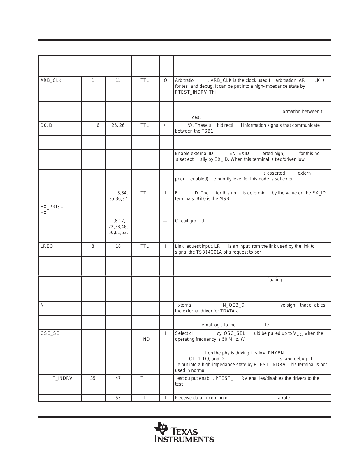
I/O DESCRIPTION
O
Arbitration clock. ARB_CLK is the clock used for arbitration. ARB_CLK is
for test and debug. It can be put into a high-impedance state by
Á
Á
Á
Á
ББББББББББББББББ
PTEST_INDRV. This terminal is not used in normal operation and is
ББББББББББББББББ
always at 49.152 MHz.
I/O
Control I/O. These are bidirectional signals that communicate between the
TSB14C01A and the link that controls passage of information between the
ББББББББББББББББ
two devices.
I/O
Data I/O. These are bidirectional information signals that communicate
between the TSB14C01A and the link layer.
ББББББББББББББББ
I
Enable priority . ENA_PRI is tied low to enable the 7-bit bus request. See
Table 1 for more information.
I
Enable external ID. When EN_EXID is asserted high, the ID for this node
is set externally by EX_ID. When this terminal is tied/driven low, the
Á
ББББББББББББББББ
source of the ID comes from the internal ID register.
I
Enable external priority . When EN_EXPRI is asserted high (external
Á
Á
ББББББББББББББББ
priority enabled) the priority level for this node is set externally (see
Table 1). This terminal should be tied low when not used.
ББББББББББББББББ
I
External ID. The ID for this node is determined by the value on the EX_ID
terminals. Bit 0 is the MSB.
I
External priority . The priority for this node is determined by the values on
the EX_PRI terminals. See Table 1 for more information.
Á
Á
Á
ББББББББББББББББ
—
Circuit ground
ББББББББББББББББ
ББББББББББББББББ
I
Link request input. LREQ is an input from the link used by the link to
signal the TSB14C01A of a request to perform some service.
—
Circuit power
Á
Á
Á
Á
ББББББББББББББББ
—
Not connected. These terminals must be left floating.
ББББББББББББББББ
ББББББББББББББББ
O
External driver enable. N_OEB_D is a negative active signal that enables
the external driver for TDATA and TSTRB.
ББББББББББББББББ
I
Logic reset input . Forcing N_POR low causes a reset condition and
resets the internal logic to the reset start state.
I
Select clock frequency. OSC_SEL should be pulled up to VCC when the
Á
ББББББББББББББББ
operating frequency is 50 MHz. When the operating frequency is 100 MHz
then it should be pulled to ground. It should not be left floating
O
Phy enable. When the phy is driving it is low, PHYENA is the control to the
Á
Á
ББББББББББББББББ
CTL0, CTL1, D0, and D1 drivers. PHYENA is for test and debug. It can
be put into a high-impedance state by PTEST_INDRV. This terminal is not
ББББББББББББББББ
used in normal operation.
I
Test output enable. PTEST_INDRV enables/disables the drivers to the
Á
ББББББББББББББББ
test terminals ARB_CLK, PHYENA, and RPREFIX. During normal
operation, PTEST_INDRV should be tied to VCC to disable the drivers.
I
Receive data. Incoming data is received at the data rate.
.
POST OFFICE BOX 655303 • DALLAS, TEXAS 75265
5
TSB14C01A, TSB14C01AI, TSB14C01AM
Á
Á
Á
Á
Á
Á
Á
Á
Á
Á
Á
Á
Á
Á
Á
Á
Á
Á
Á
Á
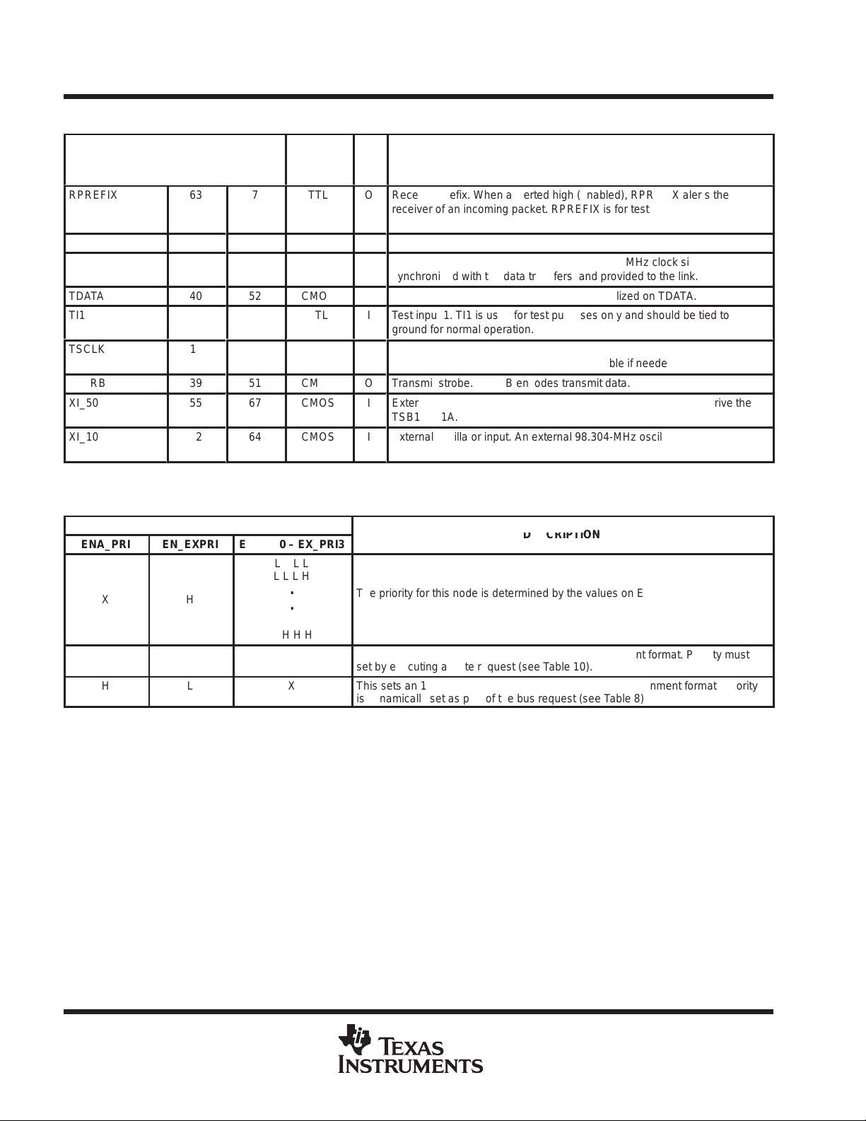
DESCRIPTION
5-V IEEE 1394-1995 BACKPLANE TRANSCEIVER/ARBITER
SGLS107A – FEBRUARY 1999 – REVISED NOVEMBER 1999
Terminal Functions (continued)
TERMINAL
NAME PM
RPREFIX
ÁÁÁÁ
RSTRB
SCLK
ÁÁÁÁ
TDATA
TI1
TSCLK
ÁÁÁÁ
TSTRB
XI_50
XI_100
ÁÁÁÁ
NO.
63
ÁÁ
42
10
ÁÁ
40
58
11
ÁÁ
39
55
52
ÁÁ
HV
NO.
7
ÁÁ
54
20
ÁÁ
52
2
21
ÁÁ
51
67
64
ÁÁ
TYPE
TTL
ÁÁ
TTL
TTL
ÁÁ
CMOS
TTL
TTL
ÁÁ
CMOS
CMOS
CMOS
ÁÁ
I/O DESCRIPTION
O
Receiver prefix. When asserted high (enabled), RPREFIX alerts the
receiver of an incoming packet. RPREFIX is for test and debug and is not
БББББББББББББББББ
used in normal operation.
I
Receive strobe. RSTRB decodes the received data.
O
System clock output. A 49.152-MHz or 24.576-MHz clock signal
synchronized with the data transfers, and provided to the link.
БББББББББББББББББ
O
Transmit data. Data to be transmitted is serialized on TDAT A.
I
Test input 1. TI1 is used for test purposes only and should be tied to
ground for normal operation.
O
System clock output. A 49.152-MHz or 24.576-MHz clock signal that is 180
degrees out of phase with SCLK; it is available if needed.
БББББББББББББББББ
O
Transmit strobe. TSTRB encodes transmit data.
I
External oscillator input. An external 49.152-MHz oscillator can drive the
TSB14C01A.
I
External oscillator input. An external 98.304-MHz oscillator can drive the
TSB14C01A.
БББББББББББББББББ
Table 1. External Priority Coding
EXTERNAL PRIORITY TERMINALS
ENA_PRI EN_EXPRI EX_PRI0 – EX_PRI3
L L L L
L L L H
X H
.
.
The priority for this node is determined by the values on EX_PRI0 – EX_PRI3.
The state of ENA_PRI can be either tied to VCC or GND.
.
H H H H
L L X This sets a 7-bit bus request and is the cable environment format. Priority must be
H L X This sets an 11-bit bus request and is the backplane environment format. Priority
set by executing a write request (see Table 10).
is dynamically set as part of the bus request (see Table 8)
6
POST OFFICE BOX 655303 • DALLAS, TEXAS 75265
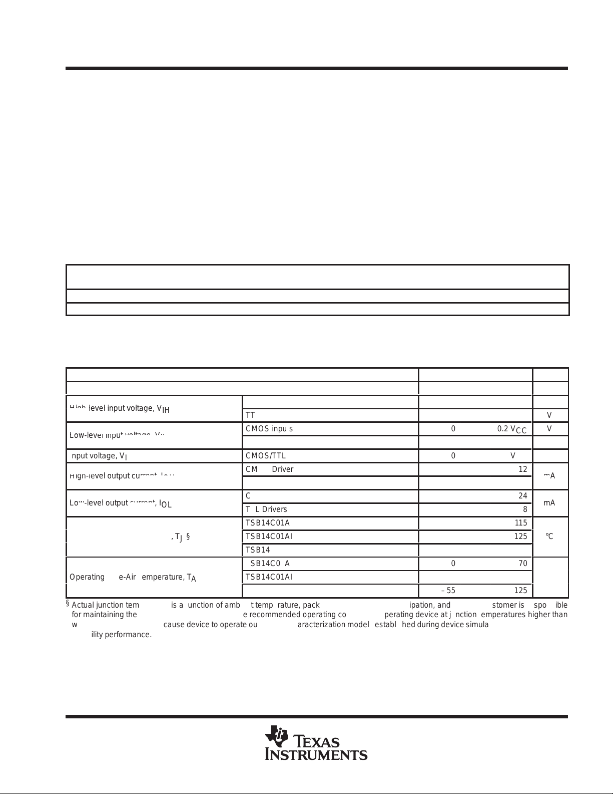
TSB14C01A, TSB14C01AI, TSB14C01AM
High-level input voltage, V
Low-level input voltage, V
High-level output current, I
mA
Low-level output current, I
mA
5-V IEEE 1394-1995 BACKPLANE TRANSCEIVER/ARBITER
SGLS107A – FEBRUARY 1999 – REVISED NOVEMBER 1999
absolute maximum ratings over operating free-air temperature range (unless otherwise noted)
Supply voltage range, V
Input voltage range, V
Output voltage range at any output, V
CC
I
O
–0.5 V to VCC + 0.5 V. . . . . . . . . . . . . . . . . . . . . . . . . . . . . . . . . . . . . . . . . . . . . . . . . . . . . .
–0.5 V to VCC + 0.5 V. . . . . . . . . . . . . . . . . . . . . . . . . . . . . . . . . . . . . . .
Continuous total power dissipation See Dissipation Rating Table. . . . . . . . . . . . . . . . . . . . . . . . . . . . . . . . . . . . . .
Operating free air temperature, TA:TSB14C01A 0°C to 70°C. . . . . . . . . . . . . . . . . . . . . . . . . . . . . . . . . . . . . . . . .
TSB14C01AI –40°C to 85°C. . . . . . . . . . . . . . . . . . . . . . . . . . . . . . . . . . . . . .
TSB14C01AM –55°C to 125°C. . . . . . . . . . . . . . . . . . . . . . . . . . . . . . . . . . . .
Storage temperature range, T
stg
Lead temperature 1,6 mm (1/16 inch) from case for 10 seconds 300°C. . . . . . . . . . . . . . . . . . . . . . . . . . . . . . . .
†
Stresses beyond those listed under “absolute maximum ratings” may cause permanent damage to the device. These are stress ratings only, and
functional operation of the device at these or any other conditions beyond those indicated under “recommended operating conditions” is not
implied. Exposure to absolute-maximum-rated conditions for extended periods may affect device reliability.
DISSIPATION RATING TABLE
PACKAGE
HV 1689 mW 13.5 mW/°C 1081 mW 879 mW 337 mW
PM 1602 mW 12.8 mW/°C 1025 mW 833 mW —
‡
This is the inverse of the traditional junction-to-ambient thermal resistance (R
and 74°C/W for the HV package.
TA ≤ 25°C
POWER RATING
DERATING FACTOR
ABOVE TA = 25°C
‡
POWER RATING
θJA
TA = 70°C
) and uses a board-mounted R
TA = 85°C
POWER RATING
of 78°C/W for the PM package
θJA
–0.5 V to 6.0 V. . . . . . . . . . . . . . . . . . . . . . . . . . . . . . . . . . . . . . . . . . . . . . . . . . . . . . . . .
–65°C to 150°C. . . . . . . . . . . . . . . . . . . . . . . . . . . . . . . . . . . . . . . . . . . . . . . . . . . .
TA = 125°C
POWER RATING
recommended operating conditions
†
MIN NOM MAX UNIT
Supply voltage, V
Input voltage, V
Virtual Junction Temperature, TJ §
Operating Free-Air Temperature, T
§
Actual junction temperature is a function of ambient temperature, package selection, power dissipation, and air flow. Customer is responsible
for maintaining the junction temperature within the recommended operating conditions. Operating device at junction temperatures higher than
what is recommended will cause device to operate outside the characterization models established during device simulation and may affect the
reliability performance.
CC
p
p
I
p
p
IH
IL
OH
OL
A
CMOS inputs
TTL input
CMOS inputs
TTL input
CMOS/TTL
CMOS Drivers
TTL Drivers
CMOS Drivers
TTL Drivers
TSB14C01A
TSB14C01AI
TSB14C01AM
TSB14C01A
TSB14C01AI
TSB14C01AM
4.5 5 5.25 V
0.7 V
CC
2
0
0
0
0
–40
–55
0.2 V
V
V
CC
CC
0.8
CC
12
24
115
125
150
70
85
125
V
V
V
V
V
8
8
°C
°C
POST OFFICE BOX 655303 • DALLAS, TEXAS 75265
7
TSB14C01A, TSB14C01AI, TSB14C01AM
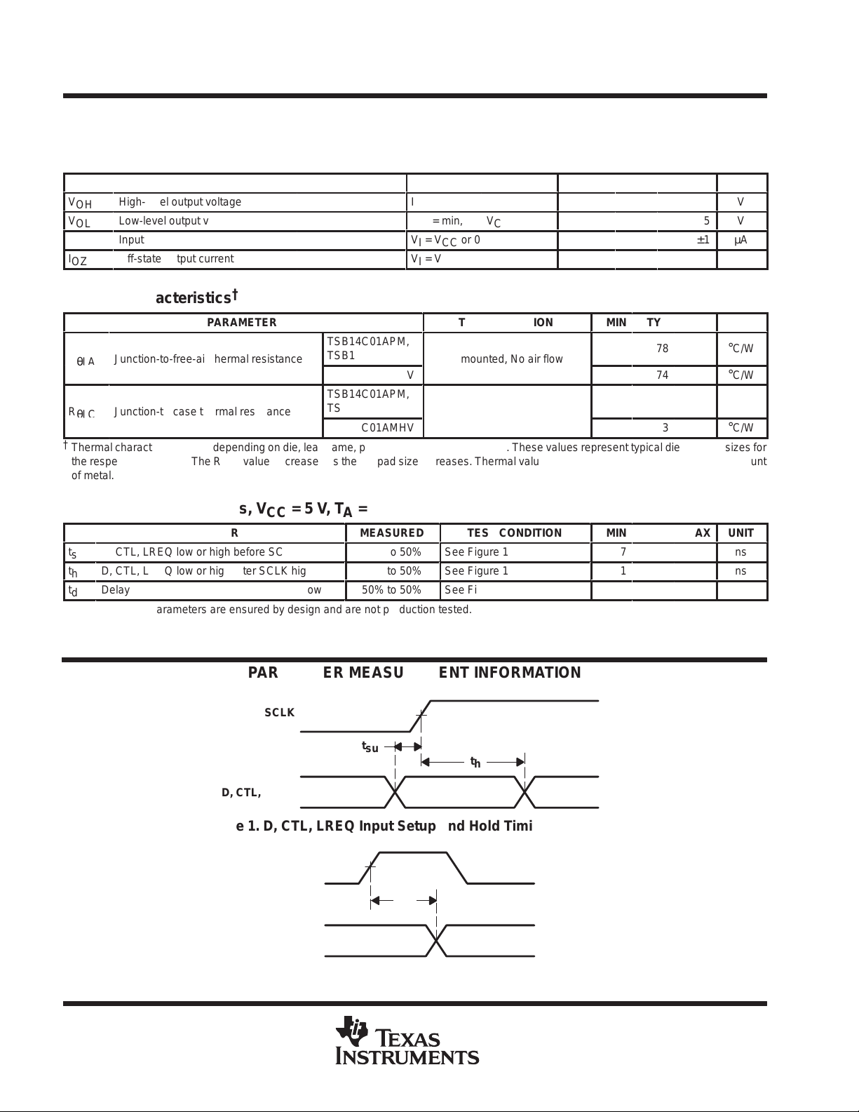
θJA
,
Á
Á
Á
Á
Á
θJC
БББББ
БББББ
БББББ
5-V IEEE 1394-1995 BACKPLANE TRANSCEIVER/ARBITER
SGLS107A – FEBRUARY 1999 – REVISED NOVEMBER 1999
electrical characteristics over recommended ranges of operating conditions (unless otherwise
noted)
device
V
V
I
OH
OL
OZ
PARAMETER TEST CONDITIONS
High-level output voltage
Low-level output voltage
Input current
Off-state output current
IOH = max,
IOL = min,
VI = VCC or 0
VI = VCC or 0
VCC = min
VCC = max
MIN TYP MAX UNIT
VCC–0.8
0.5
±1
±10
V
V
µA
µA
thermal characteristics
R
ÁÁ
R
†
Junction-to-free-air thermal resistance
ББББББББ
Junction-to-case thermal resistance
Thermal characteristics vary depending on die, leadframe, pad size, and mold compound. These values represent typical die and pad sizes for
the respective package. The R
of metal.
†
PARAMETER
TSB14C01APM,
TSB14C01AIPM
TSB14C01AMHV
TSB14C01APM,
ÁÁÁÁ
TSB14C01AIPM
TSB14C01AMHV
value decreases as the die pad size increases. Thermal values represent PWB bands with minimal amount
θJA
TEST CONDITION
MIN
TYP
Board mounted, No air flow
БББББББÁÁÁÁ
MAX
78
74
16
3
UNIT
°C/W
°C/W
°C/W
ÁÁÁ
°C/W
switching characteristics, VCC = 5 V, TA = 25°C (See Note 1)
PARAMETER
t
D, CTL, LREQ low or high before SCLK high
su
t
D, CTL, LREQ low or high after SCLK high
h
t
Delay time, SCLK high to D, CTL high or low
d
NOTE 1: These parameters are ensured by design and are not production tested.
MEASURED
50% to 50%
50% to 50%
50% to 50%
TEST CONDITION
See Figure 1
See Figure 1
See Figure 2
MIN
TYP
MAX
UNIT
7
1
10
ns
ns
ns
PARAMETER MEASUREMENT INFORMATION
8
SCLK
t
su
50%
t
h
D, CTL, LREQ
Figure 1. D, CTL, LREQ Input Setup and Hold Timing Waveforms
SCLK
D, CTL
50%
t
d
Figure 2. D, CTL Output Delay Relative to SCLK Timing Waveforms
POST OFFICE BOX 655303 • DALLAS, TEXAS 75265
TSB14C01A, TSB14C01AI, TSB14C01AM
Á
Á
Á
Á
Á
Á
Á
Á
5-V IEEE 1394-1995 BACKPLANE TRANSCEIVER/ARBITER
SGLS107A – FEBRUARY 1999 – REVISED NOVEMBER 1999
APPLICATION INFORMATION
internal register configuration
The accessible internal registers of this device are listed in Table 2. Bit field descriptions for the registers are
given in Table 3.
Table 2. Format for Registers
ADDRESS 0 1 2 3 4 5 6 7
0000 Physical
ID[0]
0001 INHB IBR RESERVED
0011 RESERVED
0100 Priority
level[0]
Physical
ID[1]
Priority
level[1]
Physical
ID[2]
Priority
level[2]
Physical
ID[3]
Priority
level[3]
Physical
ID[4]
Table 3. Register Bit Field Key
Physical
ID[5]
RESERVED
Reserved Reserved
FIELD
ÁÁÁ
Physical ID
INHB
IBR
Priority
ÁÁÁ
SIZE
(Bits)
Á
6
1
1
4
Á
TYPE
ÁÁ
Read/Write
Read/Write
Read/Write
Read/Write
ÁÁ
DESCRIPTION
ББББББББББББББББББББББ
Physical identification. Physical ID is the address of the local node and is set to zero on power up.
Inhibit Drivers. INHB is used to turn off the drivers to TDATA and TSTRB.
Initiate Bus Reset. IBR is turned on by the link and turned off by the phy when reset is complete.
Priority setting. The four bits contain the priority of the local node. A higher value in this field
ББББББББББББББББББББББ
indicates a higher priority.
transceiver selection
The system designer must select transceivers appropriate to the system requirements to be used with the
TSB14C01A and the link layer selected. The following lists requirements for the transceivers needed.
D
The transceivers used must be appropriate to the backplane technology used.
The various backplane technologies require different electrical characteristics in their backplanes. For
example BTL uses an operating voltage on the backplane of 2.1 V and a characteristic impedance of 33 Ω
while GTL uses an operating voltage of 1.2 V and a characteristic impedance of 50 Ω (see
Swing Solution for High-Speed Digital Logic
, TI literature number SCEA003). When a backplane is
designed to use BTL technology , then it would be appropriate to also use that technology for the two lines
dedicated to the 1394 serial bus. The drivers selected also must be able to supply the current required for the
expected backplane loading. For example, BTL operates correctly for a FutureBus configuration backplane
at 50 Mbits/s or for a limited number of nodes in a custom configuration at 100 Mbits/s. See the
Low Swing Solution for High-Speed Digital Logic
Bus-Interface Products
, TI literature number SCAA029, or the documentation for the transceiver being
, TI literature number SCEA003,
Understanding Advanced
considered.
GTL/BTL a Low
GTL/BTL a
D
The transceivers used must assert logic states on the backplane in an appropriate manner for the 1394
backplane arbitration.
Arbitration under 1394 backplane rules requires the drivers to assert the bus to indicate a logical 1 state, that
is a logic 1 being driven by the TSB14C01A. Conversely, the drivers should release the bus to indicate a
logic 0 state, a logic 0 being driven by the TSB14C01A. In other words, all drivers must operate in a wired-OR
mode during arbitration.
D
The transceivers used must be able to monitor the bus and drive the bus at the same time.
POST OFFICE BOX 655303 • DALLAS, TEXAS 75265
9
TSB14C01A, TSB14C01AI, TSB14C01AM
5-V IEEE 1394-1995 BACKPLANE TRANSCEIVER/ARBITER
SGLS107A – FEBRUARY 1999 – REVISED NOVEMBER 1999
During arbitration, each node that is arbitrating for the bus drives its priority code then its node number out
onto the bus. During each bit period, each node reads back what has been placed on the bus. If it reads back
the same data it was sending, the arbitrating node stays in contention for winning the bus. If it reads
something different than what it was driving, the arbitrating node loses the bus and drops out of contention.
This is the reason for requiring wired-OR operation during arbitration. As long as each node is still sending
0s onto the bus during arbitration, all nodes are still contending to win the bus. The node with the highest
priority (or if all priorities were zero then the highest node number) is the first to drive a 1 onto the bus during
arbitration. The node that sends the first 1 (asserting the bus) and reads it back wins the bus. All other nodes
read back a 1, which does not match the 0 (releasing the bus) they are sending, and drop out of contention.
This arbitration process requires the transceiver selected to be able to read from the bus at the same time it
is driving the bus.
For example, if three nodes, each with priority 0 and a node identifiers of 8, 7, and 2, were to arbitrate for the
bus, the following would occur (see Figure 3):
Driven by Node #2
(TSB14C01A)
Driven by Node #7
(TSB14C01A)
Driven by Node #8
(TSB14C01A)
Bus Data Line
(voltage level on the bus)
Bus Read
NOTE A: This bus is reverse logic, a 1 being driven by the TSB14C01A is asserted by driving a 0 onto the bus by the transceiver.
000 000
000 000
000 010
00 00
00 00
00 00
Figure 3. Three Nodes Arbitrating for the Bus
Since the highest node number is 8 (1000b), node 8 outputs the first 1 (assert the bus) and wins the
arbitration. The other nodes drop out and do not try to drive their node number onto the bus.
D
The transceivers used must be appropriate for the transfer speed required.
The 1394 bus has two data lines that use data-strobe encoding on the bus. This requires that the
transceivers be able to operate at a maximum frequency of one half of the maximum data transfer rate.
When operating at 50 Mbits/s, the maximum frequency the drivers are required to operate at is 25 MHz.
When operating at 100 Mbits/s, the maximum frequency the drivers are required to operate at is 50 MHz.
10
POST OFFICE BOX 655303 • DALLAS, TEXAS 75265

TSB14C01A, TSB14C01AI, TSB14C01AM
ÁÁ
ÁÁ
ÁÁ
ÁÁ
Á
Á
Á
Á
5-V IEEE 1394-1995 BACKPLANE TRANSCEIVER/ARBITER
SGLS107A – FEBRUARY 1999 – REVISED NOVEMBER 1999
PRINCIPLES OF OPERATION
The TSB14C01A (phy) is designed to operate with a link such as the Texas Instruments TSB12C01A. These
devices use an interface such as described in Annex J of the IEEE 1394-1995 standard. Details of how the
TSB12C01A device operates are given in the TSB12C01A data manual (literature number SLLS219). For
information on the operation of 1394, see the IEEE 1394-1995 standard. For more specific information on the
backplane phy, see the following sections of IEEE 1394-1995 standard: Chapter 5,
specification
Annex G,
; Annex D,
Backplane physical layer timing
; Annex F ,
Backplane physical implementation example
Backplane isochronous resource manager selection
. The following paragraphs describe the
operation of the phy-link interface.
The TSB14C01A supports 100 Mbit/s data transfers and has two bidirectional data lines (D0 and D1) crossing
the interface. In addition there are two bidirectional control lines (CTL0 and CTL1), the SCLK line from the phy
to the link, and the link request line (LREQ) from the link to the phy . The TSB14C01A phy has control of all the
bidirectional terminals. The link is allowed to drive these terminals only after it has been given permission by
the phy. The dedicated LREQ request terminal is used by the link for any activity that it can initiate.
There are four basic operations that can occur in the interface: request, status, transmit, and receive. All
operations but request are initiated by the phy . The link uses the request operation to read or write an internal
phy register or to ask the phy to initiate a transmit action. The phy initiates a receive action whenever a packet
is received from the serial bus.
Backplane physical layer
;
When the phy has control of the bus, the CTL0 and CTL1 lines are encoded as shown in Table 4.
Table 4. CTL0 and CTL1 Control Lines When the Phy Has Control
CTL0
CTL1
0
0
1
1
0
1
0
1
Name
Idle
Status
Receive
Transmit
Description of Activity
No activity is occurring (this is the default mode).
Status information is being sent from the phy to the link.
An incoming packet is being sent from the phy to the link.
The link has been given control of the bus to send an outgoing packet.
When the link has control of the bus (only with phy permission) the CTL0 and CTL1 lines are encoded as shown
in Table 5.
Table 5. CTL0 and CTL1 Control Lines When the Link Has Control
CTL0
0
0
Á
1
1
CTL1
0
1
Á
0
1
Name
Idle
Hold
ÁÁ
Transmit
Reserved
Description of Activity
The link releases the bus (the transmission has been completed).
The link is holding the bus while data is being prepared for transmission or sending another
ББББББББББББББББББББ
packet without arbitrating.
An outgoing packet is being sent from the link to the phy.
None
When the link needs to request the bus or access a register that is located in the TSB14C01A phy , a serial stream
of information is sent across the LREQ line. The length of the stream varies depending on whether the transfer
is a bus request, a read command, or a write command (see T able 6). Regardless of the type of transfer , a start
bit of 1 is required at the beginning of the stream, and a stop bit of 0 is required at the end of the stream. Bit 0
is the MSB, and is transmitted first. The LREQ line is required to idle low (logic level 0).
POST OFFICE BOX 655303 • DALLAS, TEXAS 75265
11

TSB14C01A, TSB14C01AI, TSB14C01AM
Á
Á
Á
Á
Á
Á
Á
Á
Á
Á
Á
Á
Á
Á
Á
Á
Á
Á
Á
Á
5-V IEEE 1394-1995 BACKPLANE TRANSCEIVER/ARBITER
SGLS107A – FEBRUARY 1999 – REVISED NOVEMBER 1999
PRINCIPLES OF OPERATION
Table 6. Request Bit Length
Request Type
ББББББ
Bus request (cable)
Bus request (backplane)
Read register request
Write register request
Number of
ÁÁÁ
Bits
7
11
9
17
For a bus request in the cable environment, the length of the LREQ data stream is 7 bits as shown in Table 7.
Table 7. Bus Request For Cable Environment
Bit(s)
0
1-3
ÁÁ
4-5
ÁÁ
ÁÁ
6
Name
Start bit
Request type
ÁÁÁÁ
Request speed
ÁÁÁÁ
ÁÁÁÁ
Stop bit
Description
Indicates the beginning of the transfer (always 1).
Indicates the type of bus request (see Table 11 for the encoding of this
БББББББББББББББББ
field).
Indicates the speed at which the phy sends the packet for this request. This
field has the same encoding as the speed code from the first symbol of the
БББББББББББББББББ
receive packet. See Table 8 for the encoding of this field. This field can be
БББББББББББББББББ
expanded to support data rates higher than 400 Mbit/s in the future.
Indicates the end of the transfer (always 0).
When LREQ transfer is a bus request in the backplane environment, it is 1 1 bits long and has the format shown
in Table 8.
Table 8. Bus Request For Backplane Environment
Bit(s)
0
1-3
ÁÁ
4-5
6-9
ÁÁ
ÁÁ
10
Name
Start bit
Request type
ÁÁÁÁ
Request speed
Request priority
ÁÁÁÁ
ÁÁÁÁ
Stop bit
Description
Indicates the beginning of the transfer (always 1).
Indicates the type of bus request (see Table 11 for the encoding of this
БББББББББББББББББ
field).
Ignored (set to 00) for the backplane environment
Indicates priority of urgent requests. It is only used with a FairReq request
type. All zeros indicates fair request.
БББББББББББББББББ
All ones is reserved (this priority is implied by a PriReq).
Other values are used to indicate the priority of an urgent request.
БББББББББББББББББ
Indicates the end of the transfer (always 0).
For a Read Register Request the length of the LREQ data stream is 9 bits as shown in T able 9 (also see T able 3
for the bit definitions).
Table 9. Read Request Format
Bit(s)
0
1-3
4-7
8
Name
Start bit
Request type
Address
Stop bit
Description
Indicates the beginning of the transfer (always 1).
Always a 100 indicating that this is a read register request.
Is the address of the phy register to be read.
Indicates the end of the transfer (always 0).
12
POST OFFICE BOX 655303 • DALLAS, TEXAS 75265
TSB14C01A, TSB14C01AI, TSB14C01AM
Á
Á
Á
Á
Á
Á
Á
Á
Á
Á
Á
Á
Á
Á
Á
5-V IEEE 1394-1995 BACKPLANE TRANSCEIVER/ARBITER
SGLS107A – FEBRUARY 1999 – REVISED NOVEMBER 1999
PRINCIPLES OF OPERATION
For a Write Register Request the length of the LREQ data stream is 17 bits as shown in Table 10 (see Table 2
for the bit field format).
Table 10. Write Request Format
Bit(s)
0
1-3
4-7
8-15
16
Name
Start bit
Request type
Address
Data
Stop bit
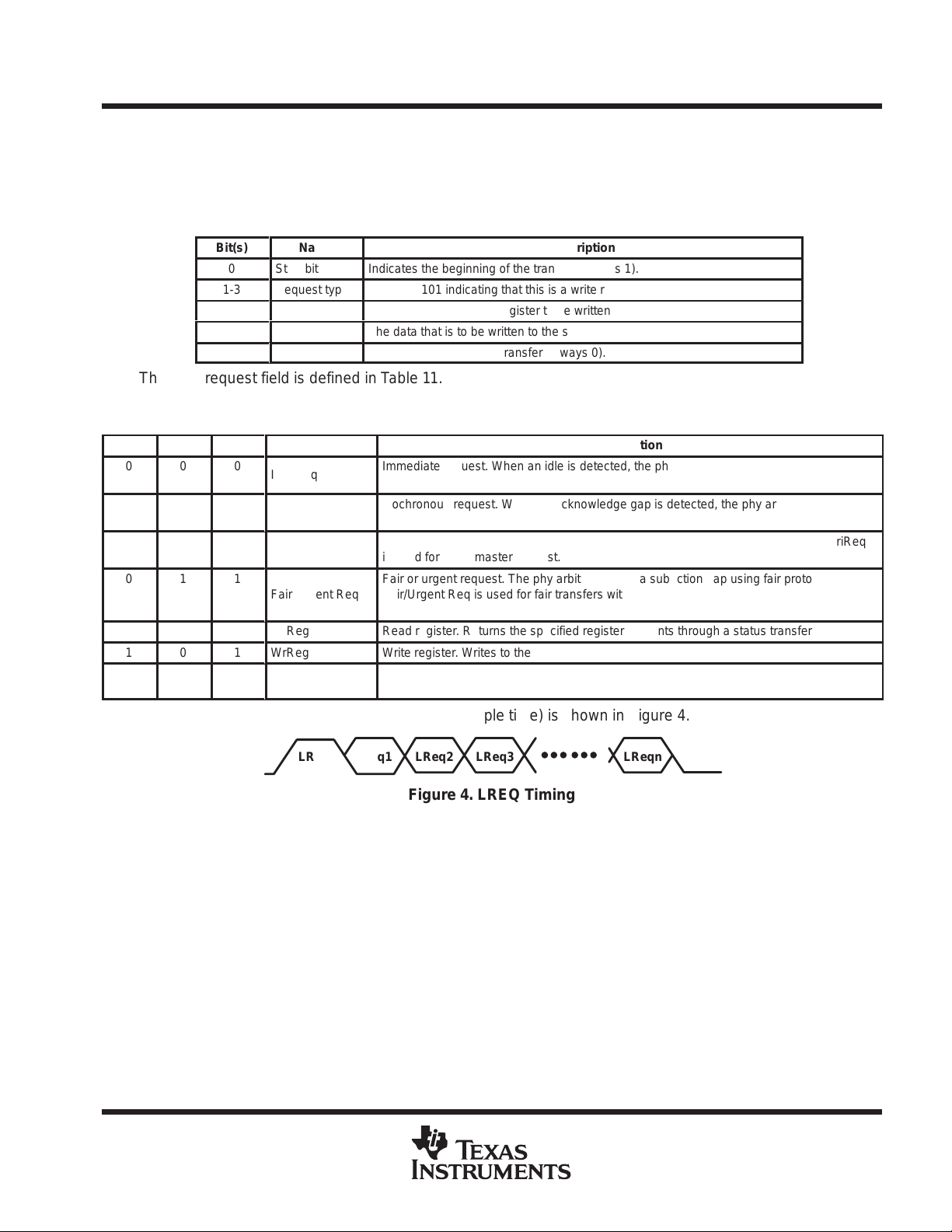
The 3-bit request field is defined in Table 11.
LREQ1
0
0
Á
0
0
Á
Á
1
1
1
Á
1
LREQ2
0
0
Á
1
1
Á
Á
0
0
1
Á
1
LREQ3
0
1
ÁÁ
0
1
ÁÁ
ÁÁ
0
1
0
ÁÁ
1
Name
ImmReq
IsoReq
ÁÁÁ
PriReq
ÁÁÁ
Fair/Urgent Req
ÁÁÁ
RdReg
WrReg
Reserved
ÁÁÁ
Description
Indicates the beginning of the transfer (always 1).
Always a 101 indicating that this is a write register request.
The address of the phy register to be written to.
The data that is to be written to the specified register address.
Indicates the end of the transfer (always 0).
Table 11. Request Field
Description
Immediate request. When an idle is detected, the phy takes control of the bus
immediately (no arbitration)
Isochronous request. When an acknowledge gap is detected, the phy arbitrates for the
bus.
ББББББББББББББББББББ
Priority request. The phy arbitrates after a subaction gap and ignore fair protocol. PriReq
is used for cycle master request.
Fair or urgent request. The phy arbitrates after a subaction gap using fair protocol.
ББББББББББББББББББББ
Fair/Urgent Req is used for fair transfers with the request priority field differentiating fair
and urgent transfers for the backplane environment.
ББББББББББББББББББББ
Read register. Returns the specified register contents through a status transfer
Write register . W rites to the specified register
Reserved
ББББББББББББББББББББ
LREQ Timing (each cell represents one clock sample time) is shown in Figure 4.
LReq0 LReq1 LReq2 LReq3 LReqn
Figure 4. LREQ Timing
POST OFFICE BOX 655303 • DALLAS, TEXAS 75265
13

TSB14C01A, TSB14C01AI, TSB14C01AM
5-V IEEE 1394-1995 BACKPLANE TRANSCEIVER/ARBITER
SGLS107A – FEBRUARY 1999 – REVISED NOVEMBER 1999
PRINCIPLES OF OPERATION
bus request
For fair or priority access, the link requests control of the bus at least one clock after the phy-link interface
becomes idle. When the link senses that the CTL terminals are in a receive state (CTL 0 and CTL1 = 10), then
it knows that its request has been lost. This is true anytime during or after the link sends the bus request transfer.
Additionally , the phy ignores any fair or priority requests if it asserts the receive state while the link is requesting
the bus. The link then reissues the request one clock after the next interface idle.
The cycle master node uses a priority request (PriReq) to send the cycle start message. To request the bus to
send isochronous data, the link can issue the request at any time after receiving the cycle start. The phy clears
an isochronous request only when the bus has been won.
T o send an acknowledge, the link must issue an ImmReq request during the reception of the packet addressed
to it. This is required because the delay from end-of-packet to acknowledge request adds directly to the
minimum delay every phy must wait after every packet to allow an acknowledge to occur. After the packet ends,
the phy immediately takes control of the bus and grants the bus to the link. If the header cyclic redundancy check
(CRC) of the packet turns out to be bad, the link releases the bus immediately . The link cannot use this grant
to send another type of packet. To ensure this, the link must wait 160 ns after the end of the received packet
to allow the phy to grant it the bus for the acknowledgement, then releases the bus and proceeds with another
request.
Although highly improbable, it is conceivable that two separate nodes can believe that an incoming packet is
intended for them. The nodes then issue an ImmReq request before checking the CRC of the packet. Since both
phys seize control of the bus at the same time, a temporary, localized collision of the bus occurs somewhere
between the competing nodes. This collision would be interpreted by the other nodes on the network as being
a ZZ line state, not a bus reset. As soon as the two nodes check the CRC, the mistaken node drops its request
and the false line state is removed. The only side effect would be the loss of the intended acknowledgment
packet (this is handled by the higher-layer protocol).
Once the link issues an immediate, isochronous, fair, or priority request for access to the bus, it cannot issue
another request until the phy indicates a lost (incoming packet) or won (transmit) signal. The phy ignores new
requests while a previous request is pending.
read/write requests
For write requests, the phy takes the value in the data field (see Table 2) of the transfer and loads it into the
addressed register as soon as the transfer is complete. For read requests (see Table 2), the phy returns the
contents of the addressed register at the next opportunity through a status transfer. The link is allowed to perform
a read or write operation at any time. When the status transfer is interrupted by an incoming packet, the phy
continues to attempt the transfer of the requested register until it is successful.
14
POST OFFICE BOX 655303 • DALLAS, TEXAS 75265

TSB14C01A, TSB14C01AI, TSB14C01AM
Á
Á
Á
Á
Á
Á
Á
Á
Á
Á
Á
Á
5-V IEEE 1394-1995 BACKPLANE TRANSCEIVER/ARBITER
SGLS107A – FEBRUARY 1999 – REVISED NOVEMBER 1999
PRINCIPLES OF OPERATION
status
When the phy has status information to transfer to the link, it initiates a status transfer. The phy waits until the
interface is idle to perform the transfer. The phy initiates the transfer by asserting status (01) on the CTL
terminals, along with the first two bits of status information on D0 and D1. The phy maintains CTL == status for
the duration of the status transfer. The phy can temporarily halt a status transfer by asserting something other
than status on the CTL terminals. This is done in the event that a packet arrives before the status transfer
completes. There must be at least one idle cycle between consecutive status transfers.
The phy normally sends only the first 4 bits of status to the link. These bits are status flags that are needed by
link state machines. The phy sends an entire status packet to the link after a request transfer that contains a
read request.
The definition of the bits in the status transfer are shown in Table 12 (also see Table 2 and Table 9). The 16-bit
status stream is defined in Table 12.
Table 12. Status Bit Description
Phy
CTL0, CTL1
Phy
D0, D1
Bit(s)
0
ÁÁ
1
ÁÁ
ÁÁ
2
3
4-7
ÁÁ
8-15
Name
Arbitration
ÁÁÁ
Reset gap
Indicates that the phy has detected that the bus has been idle for an
БББББББББББББББББ
arbitration reset gap time (this time is defined in the 1394 standard). This bit
Description
is used by the link in its busy/retry state machine.
Subaction gap
ÁÁÁ
ÁÁÁ
Bus reset
Reserved
Address
ÁÁÁ
Data
00 01 01 01 00 00
00 S[0,1] 00 00
Indicates that the phy has detected that the bus has been idle for a subaction
БББББББББББББББББ
gap time (this time is defined in the 1394 standard). This bit is used by the
link to detect the completion of an isochronous cycle.
БББББББББББББББББ
Indicates that the phy has entered the bus reset state.
Reserved
Holds the address of the phy register whose contents are transferred to the
БББББББББББББББББ
link.
Indicates the data that is to be sent to the link.
00
00
S[2,3]
S[14,15]
Figure 5. Status Transfer Timing
POST OFFICE BOX 655303 • DALLAS, TEXAS 75265
15

TSB14C01A, TSB14C01AI, TSB14C01AM
5-V IEEE 1394-1995 BACKPLANE TRANSCEIVER/ARBITER
SGLS107A – FEBRUARY 1999 – REVISED NOVEMBER 1999
PRINCIPLES OF OPERATION
transmit
When the link requests access to the serial bus through the LREQ terminal, the phy arbitrates for access to the
serial bus. When the phy wins the arbitration, it grants the bus to the link by asserting transmit on the CTL
terminals for one SCLK cycle, followed by idle for one cycle. After sampling the transmit state from the phy, the
link takes over control of the interface by asserting either hold or transmit on the CTL terminals. The link asserts
hold to keep ownership of the bus while preparing data. The phy asserts the data-on state on the serial bus
during this time. When it is ready to begin transmitting a packet, the link asserts transmit on the CTL terminals
along with the first bits of the packet. After sending the last bits of the packet, the link asserts either idle or hold
on the CTL terminals for one cycle, and then idle for one additional cycle, before asserting those terminals to
a high-impedance state.
The hold state here indicates to the phy that the link needs to send another packet without releasing the bus.
The phy responds to this hold state by waiting the required minimum time and then asserting transmit as before.
This function would be used after sending an acknowledgement if the link intends to send a unified response,
or to send consecutive isochronous packets during a single cycle. The only requirement when sending multiple
packets during a single bus ownership is that all packets must be transmitted at the same speed, since the speed
of the packet transmission is set before the first packet.
As noted above, when the link has finished sending the last packet for the current bus ownership, it releases
the bus by asserting idle on the CTL terminals for two SCLK cycles. The phy begins asserting idle on the CTL
terminals one clock after sampling the second idle from the link. Note that whenever the D and CTL lines change
ownership between the phy and the link, there is an extra clock period allowed so that both sides of the interface
can operate on registered versions of the interface signals, rather than having to respond to a CTL state on the
next cycle.
It is not required that the link enter the hold state before sending the first packet when implementation permits
the link to be ready to transmit as soon as bus ownership is granted. The timing for a single packet transmit
operation is shown in Figure 6. In the diagram, D0 – Dn are the data symbols of the packet; ZZ represents the
high-impedance state.
16
POST OFFICE BOX 655303 • DALLAS, TEXAS 75265
transmit timing
Single Packet
Phy
CTL0, CTL1
Phy
D0, D1
Link
CTL0, CTL1
Link
D0, D1
Continued Packet
Phy
CTL0, CTL1
Phy
D0, D1
Link
CTL0, CTL1
Link
D0, D1
NOTE A: ZZ = High Impedance State
D0 = > Dn = Packet data
11 00 ZZ ZZ ZZ ZZ
00 00 ZZ ZZ ZZ ZZ
ZZ ZZ 01 10 10 10
ZZ ZZ 00 D0 D1 D2
ZZ
TSB14C01A, TSB14C01AI, TSB14C01AM
5-V IEEE 1394-1995 BACKPLANE TRANSCEIVER/ARBITER
SGLS107A – FEBRUARY 1999 – REVISED NOVEMBER 1999
ZZ ZZ 00 11 00 ZZ
ZZ ZZ 00 00 00 ZZ
01 00 ZZ ZZ ZZ 01
00 00 ZZ ZZ ZZ 00
ZZ ZZ 00ZZ ZZ00
ZZ ZZ 00ZZ ZZ00
00 00 ZZ01 10ZZ
00 00 ZZ00 DnZZ
ZZ ZZ ZZ00ZZ
ZZ ZZ ZZ00ZZZZ
01 10 10ZZ1010
00 D0 D1ZZDnDn-1
Figure 6. Transmit Timing
receive
When data is received by the phy from the serial bus, it transfers the data to the link for further processing. The
phy asserts receive (see T able 4) on the CTL lines and asserts each D terminal high. The phy indicates the start
of the packet by placing the speed code on the data bus. The phy then proceeds with the transmittal of the packet
to the link on the D lines while still keeping the receive status on the CTL terminals. Once the packet has been
completely transferred, the phy asserts idle on the CTL terminals, which completes the receive operation (see
Figure 7).
NOTE
The speed code is a phy-link protocol and is not included in the CRC.
Phy
CTL0, CTL1
Phy
D0, D1
NOTE A: SPD = Speed Code (For the backplane, this speed is fixed at D0, D1 = 00).
D0 to Dn = Packet data
10 10 10 10
11 SPD D0 D1
Figure 7. Receive Timing
10 00 001000
Dn 00 001100
POST OFFICE BOX 655303 • DALLAS, TEXAS 75265
17

TSB14C01A, TSB14C01AI, TSB14C01AM
5-V IEEE 1394-1995 BACKPLANE TRANSCEIVER/ARBITER
SGLS107A – FEBRUARY 1999 – REVISED NOVEMBER 1999
PRINCIPLES OF OPERATION
backplane phy connection
Within the backplane environment the serial bus is implemented with a pair of signals (STRB and DA TA). The
topology is a simple pair of bussed signals as shown in Figure 8.
Backplane Chassis
Module
Node
PHY
NOTE A: On a given bus, there can be as many as 63 nodes. There is no restriction on the distribution of nodes
throughout modules on the bus. When more than one node occupies a module, they must share the
same transceivers.
Module
Node
PHY
STRB
DATA
Node
PHY
Module
Node
PHY
Node
PHY
Module
Node
PHY
Figure 8. Backplane Topology
The backplane environment can be implemented with a number of different interface technologies. These
include, but are not limited to: TTL for industry-standard transistor-transistor logic, BTL for backplane
transceiver logic as defined by IEEE Std 1194.1, and ECL for emitter-coupled logic.
In addition to the requirements specified by the application environment, the physical media of the serial bus
should meet the requirements defined for media attachment, media signal interface, and media signal timing.
Timing requirements must be met over the ranges specified in the application environment. These include
temperature ranges, voltage ranges, and manufacturing tolerances.
18
POST OFFICE BOX 655303 • DALLAS, TEXAS 75265

TSB14C01A, TSB14C01AI, TSB14C01AM
5-V IEEE 1394-1995 BACKPLANE TRANSCEIVER/ARBITER
SGLS107A – FEBRUARY 1999 – REVISED NOVEMBER 1999
PRINCIPLES OF OPERATION
definition of logic states
Drivers assert the bus to indicate a 1 logic state, or release the bus to indicate a 0 logic state. T o assert the bus,
a driver sinks current. T o release the bus, drivers are asserted to a high-impedance state or turned off, allowing
the bus signal to be pulled to the termination voltage of the bus.
NOTE
This typically results in a logical inversion of signals on TTL and BTL buses. Signals on ECL buses
typically are not inverted.
All drivers operate in a wired-ORed or open-collector mode during arbitration. Drivers can operate in a totem
pole mode during data packet and acknowledge transfers. In this mode, a driver can drive the bus into its
released state in order to decrease the rise time of the bus signal (referred to as a rescinding release with TTL
technology).
bit rates
Data transmission and reception occurs at 49.152 Mbit/s or 98.304 Mbit/s (±100 ppm). Regardless of the
interface technology, arbitration occurs at an arbitration clock rate of 49.152 MHz.
backplane transmit data timing
Edge separation is the minimum required time between any two consecutive transitions of the backplane bus
signals, as they appear from the output of the transmitters, whether they be transitions on the same signal or
transitions on the two separate signals. A minimum edge separation is required to ensure proper operation of
the data strobe bit-level encoding mechanism. TDA T A and TSTRB have the relationship shown in Figure 9 and
Table 13.
t1 t1 t1 t1
TDATA
t2 t2 t2 t2
TSTRB
Figure 9. Minimum Edge Separation
Table 13. TSB14C01A to Backplane Transceiver Timing
PARAMETER
t1
Bit cell period for data
t2
Transmit (Tx) edge separation
98.304 MHz
9.44 ns minimum
8.65 ns minimum
49.152 MHz
19.44 ns minimum
18.65 ns minimum
POST OFFICE BOX 655303 • DALLAS, TEXAS 75265
19

TSB14C01A, TSB14C01AI, TSB14C01AM
5-V IEEE 1394-1995 BACKPLANE TRANSCEIVER/ARBITER
SGLS107A – FEBRUARY 1999 – REVISED NOVEMBER 1999
PRINCIPLES OF OPERATION
backplane receive data timing
The receiver typically uses the transitions on the incoming bus signals RDATA and RSTRB to derive a clock
at the code bit frequency to extract the NRZ signal on RDATA. This clock can be derived by performing an
exclusive-OR (XOR) of RDATA and RSTRB.
The bus signals, as they appear from the backplane transceiver media and into the receivers, should be within
the constraints outlined by Figure 10.
t1 t1 t1 t1
RDATA
t3 t2 t3 t2
RSTRB
Figure 10. Backplane Receive Data Timing
Table 14. TSB14C01A to Backplane Transceiver Timing
PARAMETER
t1
t2
t3
†
This parameter is based on a maximum total transmit skew of 2 ns and a maximum backplane skew
of 0.5 ns. This assumes total receive skew is less than receive edge separation (i.e., some skew
margin exists).
Bit cell period
†
Receive (Rx) edge separation
Receive (Rx) edge separation
backplane timing definitions
D
Logic Skew — The skew between data and strobe within the physical layer itself due to internal skews
between data and strobe logic.
D
Spatial Skew — The skew between data and strobe due to differences in propagation delays along the
transmission line from arbiter to transceiver. This board delay is of concern when the physical layer and
transceivers are packaged separately.
D
Package Skew — The propagation delay difference through the transceiver between the data and strobe
channels.
D
Backplane Skew — The skew along the backplane itself due to impedance and/or mismatching of lengths
in the data and strobe lines.
D
Receive Setup/Hold — The setup and hold time needed to latch in the incoming data within the phy arbiter,
based off of the recovered clock from Data-Rx and Strobe-Rx.
98.304 Mhz
10.1715 ns nominal
3.4 ns minimum
16.3 ns maximum
49.152 MHz
20.34 ns nominal
3.4 ns minimum
36.6 ns maximum
20
D
T otal T ransmit Skew — The total skew between data and strobe in transmitting data from the phy out to the
bus. This is given by the following equation.
POST OFFICE BOX 655303 • DALLAS, TEXAS 75265

D
T otal Receive Skew — The total skew between data and strobe in receiving data from the bus into the phy.
This is given by the following equation.
D
Skew Margin — The bit cell period minus all skews. This is given by the following equation.
D
Transmit Edge Separation — The minimum time required between any two consecutive transitions of the
bus signals to ensure proper operation of data-strobe bit level encoding. Transmit edge separation is
measured from the midpoint of the signal transition to the midpoint of the next signal transition out on the
bus. Minimum transmit edge separation is the minimum bit cell period less the maximum total transmit skew.
D
Receive Edge Separation — The minimum time required between any two consecutive transitions of the
bus signals to ensure proper operation of data-strobe bit level decoding. Receive edge separation is
measured from the midpoint of the signal transition to the midpoint of the next signal transition out on the
bus. This is the minimum bit cell period reduced by the amount of maximum total transmit skew and
maximum backplane skew.
gap timing
TSB14C01A, TSB14C01AI, TSB14C01AM
5-V IEEE 1394-1995 BACKPLANE TRANSCEIVER/ARBITER
SGLS107A – FEBRUARY 1999 – REVISED NOVEMBER 1999
Total Transmit Skew+Transmit Package Skew)Spatial Skew)Logic Skew
Total Receive Skew+Receive Package Skew)Spatial Skew)Receive Setup)Receive Hold
Skew Margin+Bit Cell Period*Total Transmit Skew*Backplane Skew*Total Receive Skew
A gap is a period of time during which the bus is idle (Data_Rx and Strb_Rx are unasserted). There are three
types of gaps:
D
Acknowledge Gap — Appears between the end of a packet and an acknowledge, as well as between
isochronous transfers. A node should detect the occurrence of an acknowledge gap after the bus has been
in an unasserted state for 4 arbitration clock times (approximately 81.38 ns), but should not assert the bus
until a total of 8 arbitration clock times (approximately 182.76 ns) have occurred. This requirement ensures
that a node is given adequate time to detect the acknowledge gap before the bus is asserted by another
node upon detecting an acknowledge gap. This includes the minimum time required to detect a BUS_IDLE
(4 arbitration clock times), as well as the maximum delay between the arbitration state machines within any
two nodes on the bus (another 4 arbitration clock times).
D
Subaction Gap — Appears before asynchronous transfers within a fairness interval. A node should detect
the occurrence of a subaction gap after the bus has been in an unasserted state for at least 16 arbitration
clock times (approximately 325.52 ns), but should not assert the bus until a total of 20 arbitration clock times
(approximately 406.9 ns) have occurred. This requirement ensures that a node is given adequate time to
detect the subaction gap before the bus is asserted by another node (upon detecting a subaction gap). The
duration of the subaction gap ensures that another node asserting the bus after an acknowledge gap has
been detected by this time.
D
Arbitration Reset Gap — Appears before asynchronous transfers when the fairness interval starts. A node
should detect the occurrence of an arbitration reset gap after the bus has been in an unasserted state for
at least 28 arbitration clock times (approximately 569.66 ns), but should not assert the bus until a total of
32 arbitration clock times (approximately 651.04 ns) have occurred. This requirement ensures that a node
is given adequate time to detect the arbitration reset gap before the bus is asserted by another node (upon
detecting an arbitration reset gap). The duration of the arbitration reset gap ensures that another node
asserting the bus after a subaction gap or an acknowledge gap has been detected by this time.
If a node is waiting for the occurrence of a particular gap, and the bus has become idle for the specified time
(e.g., 32 arbitration clock times for an arbitration reset gap), the node detects the gap and asserts the bus within
the time constraints described under the bus synchronization and propagation delay section of this document.
These constraints ensure that an asserted signal propagates through the node decision/transceiver circuitry
and onto the bus soon enough to allow arbitration to occur properly.
POST OFFICE BOX 655303 • DALLAS, TEXAS 75265
21

TSB14C01A, TSB14C01AI, TSB14C01AM
5-V IEEE 1394-1995 BACKPLANE TRANSCEIVER/ARBITER
SGLS107A – FEBRUARY 1999 – REVISED NOVEMBER 1999
PRINCIPLES OF OPERATION
arbitration sequence
The arbitration sequence is the process that the TSB14C01A uses to arbitrate the bus between competing
modules.
arbitration number
The arbitration sequence uses a unique arbitration number for each module. This 6-bit number is the same as
the node physical_ID. When less than 6 bits are provided for the arbitration number, they occupy the MSBs of
the arbitration number. The remaining bits are zero-filled. The MSBs are transmitted first.
NOTE
If the serial bus is contained within a host backplane, it is expected that the arbitration number (i.e.,
physical_ID) is set by the host backplane at power up (e.g., with a built-in slot identifier or
configuration mechanism).
It is recommended that this number be software programmable to facilitate testing and to allow for consistent
system operation and repeatability.
priority
Within the arbitration sequence, the arbitration number is preceded by four bits that define a priority level. The
method by which priority is assigned is to be determined by the system integrator with two exceptions. The
lowest priority (all zeros) is reserved for fair arbitration and the highest priority (all ones) is reserved for cycle
start requests. This allows 14 priority levels to be used for the urgent arbitration process.
The use of an urgent priority class allows nodes to be granted a larger portion of the bandwidth on the bus. High
priority nodes are granted the bus before lower priority nodes during urgent allocation of the bus, allowing such
nodes to be granted more bandwidth.
In order to ensure forward progress, the lowest priority level is reserved for fair arbitration. This allows all nodes
arbitrating with this priority level to be allowed one fair access to the bus for each fairness interval. For fair
arbitration, the value of the arbitration number has a minimal impact on the allocation of the bus. Although nodes
with higher arbitration numbers are granted the bus sooner, there is only a small decrease in latency.
The 4-bit priority field is not used in isochronous arbitration. When arbitrating for an isochronous transfer, the
priority field is zero-filled.
22
POST OFFICE BOX 655303 • DALLAS, TEXAS 75265

5-V IEEE 1394-1995 BACKPLANE TRANSCEIVER/ARBITER
PRINCIPLES OF OPERATION
format of arbitration sequence
The following format for the arbitration sequence should be used:
PRIORITY ARBITRATION NUMBER
4 bits 6 bits
arbitration sequence
D
Each module on the backplane has a unique 6-bit arbitration number that is equal to the node’s physical_ID.
D
The arbitration number is preceded by four bits of priority . The MSB of the priority field is transmitted first.
The LSB of the priority field is followed by the MSB of the arbitration number.
D
Dynamic assignment of priority is accommodated.
D
The lowest priority level (all zeroes) is reserved for fair arbitration, and the highest priority level (all ones)
is reserved for the identification of the cycle start packet.
arbitration
TSB14C01A, TSB14C01AI, TSB14C01AM
SGLS107A – FEBRUARY 1999 – REVISED NOVEMBER 1999
Unless a node is using immediate arbitration to access the bus (in which case there is no contention for the bus),
it is possible that more than one node can attempt to access the bus at a given time. Consequently, it is
necessary for a node to arbitrate for the bus in order to gain access to the bus.
NOTE
A node uses immediate arbitration to send an acknowledge. Since there is no contention for the
bus in this case, arbitration is not necessary . A node that is transmitting an acknowledge does not
arbitrate for the bus, but merely waits for an acknowledge gap to be detected before it begins
transmission. If a node is attempting to gain access to the bus without using immediate access, it
must first arbitrate for the bus.
Arbitration occurs in response to a phy arbitration request from the link. Nodes begin arbitrating once the bus
has become idle for a predetermined amount of time (the appropriate gap indication occurs). Once this happens,
nodes begin a bit-by-bit transmission of their arbitration sequence.
A node can obtain access to the bus in a limited number of ways. Since some arbitration classes allow nodes
to begin arbitration before others, nodes arbitrating with certain arbitration classes can detect that the bus is
busy before they can begin to arbitrate. In this way , certain arbitration classes can be bypassed. For example,
fair and urgent nodes do not get a chance to arbitrate when another node is sending an acknowledge or when
it is arbitrating for an isochronous transfer.
The backplane environment supports the fair, urgent, cycle_master, isochronous, and immediate arbitration
classes.
fairness intervals
The fairness protocol is based on the concept of a fairness interval. A fairness interval consists of one or more
periods of bus activity separated by short idle periods called subaction gaps and is followed by a longer idle
period known as an arbitration reset gap. At the end of each gap, bus arbitration is used to determine the next
bus owner. This concept is shown in Figure 11.
POST OFFICE BOX 655303 • DALLAS, TEXAS 75265
23

TSB14C01A, TSB14C01AI, TSB14C01AM
5-V IEEE 1394-1995 BACKPLANE TRANSCEIVER/ARBITER
SGLS107A – FEBRUARY 1999 – REVISED NOVEMBER 1999
PRINCIPLES OF OPERATION
fairness intervals (continued)
Fairness
Interval (N –1)
Arbitration
Reset Gap
ack
Fairness Interval (N)
Owner A Owner B Owner M
arb
Subaction
data
ack
arb
data
Subaction Gaps Arbitration
ack
arb
ack
arb
data
ack
Reset Gap
Fairness
Interval (N +1)
arb
Figure 11. Fairness Interval
The implementation of the fair arbitration protocol is defined in terms of these fairness intervals as discussed
in the following paragraphs.
fair arbitration
When using this arbitration class, an active node can send an asynchronous packet only once each fairness
interval. Once a subaction gap is detected, a node can begin arbitration when its arbitration_enable signal is
set. The arbitration_enable signal is set at the beginning of the fairness interval and is cleared when the node
successfully accesses the bus through fair arbitration. This disables further fair arbitration attempts by that node
for the remainder of the fairness interval. In the absence of urgent nodes, a fairness interval ends once all of
the nodes attempting fair arbitration have successfully accessed the bus. At this time, all of the fair nodes have
their arbitration_enable signals reset and cannot arbitrate for the bus. The bus remains idle until an arbitration
reset gap occurs. Once this happens, the next fairness interval begins. All of the nodes set their
arbitration_enable signal and can begin to arbitrate for the bus. This process is illustrated in Figure 12.
Fairness
Interval (N –1)
Fairness Interval (N)
Fairness
Interval (N +1)
arb arb
Node A
Arbitration
Enable
NOTE A: The arbitration number of A > B > C.
Node B
Node C
Arbitration
Reset Gap
Set at Arbitration Reset Gap
node A
Cleared When Node Wins Arbitration
node B
arb
node C
Figure 12. Fair Arbitration Timing
Note that a node sending a concatenated subaction does not reset its arb_enable bit.
arb
Arbitration
Reset Gap
24
POST OFFICE BOX 655303 • DALLAS, TEXAS 75265

TSB14C01A, TSB14C01AI, TSB14C01AM
5-V IEEE 1394-1995 BACKPLANE TRANSCEIVER/ARBITER
SGLS107A – FEBRUARY 1999 – REVISED NOVEMBER 1999
PRINCIPLES OF OPERATION
urgent arbitration
The backplane environment enhances the fair priority algorithm by splitting access opportunities among nodes
based on two priority classes: fair and urgent. Nodes using an urgent priority can use up to three-fourths of the
access opportunities, with the remaining ones equally shared among nodes using the fair priority . All nodes are
required to implement the fair priority class, while the urgent priority class is optional. Packets are labeled as
urgent when that priority class was used.
The fair/urgent allocation uses the same fairness interval described in fair arbitration but accompanies the
arbitration_enable flag with an urgent_count. The fair/urgent method works as follows:
D
When the bus is idle for longer than an arbitration reset gap, a fairness interval begins and all nodes set
their arbitration_enable flags, while nodes implementing urgent priority set their urgent_count to three.
D
A node that is waiting to send a packet using the fair priority class should begin arbitrating after detecting
a subaction gap as long as its arbitration_enable flag is set. When its arbitration_enable flag is cleared, it
waits for an arbitration reset gap before it begins arbitrating. When such a node wins an arbitration contest,
it sends a packet without the urgent label and its arbitration_enable flag is cleared.
D
A node that is waiting to send a packet with urgent priority begins arbitrating after detecting a subaction gap
if its urgent_count is nonzero. When its urgent_count is zero, it waits for an arbitration reset gap before it
begins arbitrating. Whenever such a node wins an arbitration contest, it sends a packet with the urgent label.
D
A node implementing urgent priority sets its urgent_count to three whenever an unlabeled (i.e., fair) packet
is transmitted or received. This includes received packets that are addressed to other nodes.
D
A node decrements its urgent_count whenever a packet with the urgent label is transmitted or received. This
includes received packets that are addressed to other nodes. This ensures that there is at most three urgent
packets for every fair packet. This does not ensure that every node using urgent priority obtains the bus
three times for each fairness interval. The node arbitrating with the highest priority always obtains the bus
before other nodes arbitrating with an urgent, but lower, priority.
In the presence of urgent nodes, a fairness interval ends after the final fair node and up to three remaining urgent
nodes have successfully accessed the bus. Since all fair nodes now have their arbitration_enable signals reset
and all urgent nodes have their urgent_count decremented to zero, none of the nodes can access the bus. The
bus remains idle until an arbitration reset gap has occurred, re-enabling arbitration on all nodes and starting the
next fairness interval. This process is illustrated in Figure 13, which illustrates a situation where there are three
nodes arbitrating for the bus with physical_IDs such that A has the highest priority, B is in the middle priority,
and C has the lowest priority, with nodes A and C using fair priority and B using urgent:
POST OFFICE BOX 655303 • DALLAS, TEXAS 75265
25

TSB14C01A, TSB14C01AI, TSB14C01AM
5-V IEEE 1394-1995 BACKPLANE TRANSCEIVER/ARBITER
SGLS107A – FEBRUARY 1999 – REVISED NOVEMBER 1999
PRINCIPLES OF OPERATION
urgent arbitration (continued)
A Node Using The Urgent
Protocol Has a Higher Priority
Fairness
Interval (N –1)
Than Any Fair Node
Urgent
Packet
Node B
arb
arb
Urgent
Packet
Node B
Fairness Interval (N)
Urgent
Packet
Node B
arb
arb
Fair
Packet
Node A
arb
Urgent
Packet
Node B
arb
Urgent
Packet
Node B
Arbitration_Enable
Node A
Node B
Urgent_Count
Node C
Arbitration_Enable
Urgent_Count Set
To 3 At Arbitration
Reset Gap
32 1 32
Arbitration
Reset Gap
Node A
Node B
Arbitration_Enable Set
at Arbitration Reset Gap
Urgent
Packet
Node B
arb
Arbitration_Enable Set At
Arbitration Reset Gap
Urgent_Count Incremented By
3 After A Fair Node (A) Wins
Arbitration and Sends A Packet
Urgent_Count Decremented
When Urgent Node Sends A Packet
Fairness Interval (N)
arb
Fair
Packet
Node C
Urgent
Packet
Node B
arb arb
Urgent_Count Incremented By 3
After A Fair Node (C) Wins Arbitration
and Sends A Packet
32 1 3
arb
Urgent
Packet
Node B
Arbitration_Enable Set At
Arbitration Reset Gap
Urgent
Packet
Node B
1
Fairness
Interval (N +1)
26
Node C
Arbitration
Reset Gap
Figure 13. Urgent Arbitration
POST OFFICE BOX 655303 • DALLAS, TEXAS 75265

TSB14C01A, TSB14C01AI, TSB14C01AM
5-V IEEE 1394-1995 BACKPLANE TRANSCEIVER/ARBITER
SGLS107A – FEBRUARY 1999 – REVISED NOVEMBER 1999
PRINCIPLES OF OPERATION
urgent arbitration (continued)
In the backplane environment, the natural priority is the concatenation of the 4-bit urgent priority level with the
physical_ID. These results are listed in the following list.
D
A node using the urgent priority always wins an arbitration contest over all nodes using the fair priority.
D
The node using the highest priority level wins the arbitration contest.
D
When more than one node uses the highest priority level, then the one with the highest physical_ID wins.
arbitration by the cycle_master
This arbitration class is used by the cycle_master when it needs to arbitrate for the transmission of a cycle_start
packet. It is similar to the urgent arbitration class, except that the priority field is defined to be all ones. Arbitration
begins once a subaction gap is detected, regardless of the state of the arbitration_enable signal or the
urgent_count.
isochronous arbitration
This arbitration class is used by nodes arbitrating to send isochronous packets. Arbitration begins once an
acknowledge gap is detected, regardless of the state of the arbitration_enable signal or the urgent_count.
Because an acknowledge gap is shorter than an arbitration reset gap and a subaction gap, nodes arbitrating
with this class win the bus before nodes waiting to send fair, urgent, or cycle_master packets. The priority field
is not used in this arbitration class.
immediate arbitration
This arbitration class is used by nodes sending an acknowledge to a received packet. Transmission of the
acknowledge (beginning with a DATA_PREFIX) occurs as soon as an acknowledge gap is detected. This
arbitration class is referred to as immediate because an arbitration sequence is not transmitted to obtain access
to the bus (i.e., the node does not actually arbitrate for the bus).
backplane phy reset
Upon a power_reset event (i.e., power up), registers and control and status registers (CSRs) associated with
the operation of the phy are initialized to their default values. State machines associated with phy operations
are initialized. The BUS_RESET signal is not transmitted on the bus by the phy.
POST OFFICE BOX 655303 • DALLAS, TEXAS 75265
27

TSB14C01A, TSB14C01AI, TSB14C01AM
5-V IEEE 1394-1995 BACKPLANE TRANSCEIVER/ARBITER
SGLS107A – FEBRUARY 1999 – REVISED NOVEMBER 1999
PRINCIPLES OF OPERATION
bus reset
Once a phy control request of bus reset is communicated from the node controller to the phy , the registers and
CSRs associated with the operation of that phy are initialized to their default values. State machines associated
with phy operations can be initialized. The phy communicates a BUS_RESET onto the bus. After the
BUS_RESET event is detected by the node transmitting it (i.e., approximately 320 arbitration clock times after
the signal is initiated), the phy initializes itself.
NOTE
Since a phy transmitting a BUS_RESET must also react accordingly once the BUS_RESET event
is detected, its state machines do have the opportunity to advance beyond those of other nodes.
This ensures that all nodes are in somewhat similar states after such a bus reset event. Obviously ,
the logic (e.g., counters) used within the phy to generate the BUS_RESET signal must not be reset
once that phy simultaneously detects its own BUS_RESET.
Once a phy detects that a BUS_RESET event has occurred on the bus, it initializes itself. The node controller
initiates a bus reset by writing to the phy control register with the IBR bit set to 1. The phy hardware resets the
IBR bit to zero on detection of its own bus reset.
live insertion
It is up to the user to design their node or module to safely receive power from the particular backplane they
are using during a live insertion or tap-in. But in principal, live insertion is supported and does not cause a
bus-reset event to occur. Please see the TI application note,
Live Insertion
, TI literature number SDYA012.
28
POST OFFICE BOX 655303 • DALLAS, TEXAS 75265

TSB14C01A, TSB14C01AI, TSB14C01AM
5-V IEEE 1394-1995 BACKPLANE TRANSCEIVER/ARBITER
SGLS107A – FEBRUARY 1999 – REVISED NOVEMBER 1999
MECHANICAL INFORMATION
HV (S-GQFP-F68) CERAMIC QUAD FLATPACK
61
1.500 (38,10)
1.300 (33,02)
60 44
1
9
SQ
43
27
0.025 (0,635)
0.013 (0,330)
0.008 (0,203)
0.400 (10,16) TYP
0.500 (12,70)
0.485 (12,32)
0.154 (3,912)
0.134 (3,404)
NOTES: A. All linear dimensions are in inches (millimeters).
B. This drawing is subject to change without notice.
C. This package can be hermetically sealed with a ceramic lid using glass frit.
2610
SQ
0.007 (0,178)
0.005 (0,127)
4040072/C 04/96
POST OFFICE BOX 655303 • DALLAS, TEXAS 75265
29

TSB14C01A, TSB14C01AI, TSB14C01AM
5-V IEEE 1394-1995 BACKPLANE TRANSCEIVER/ARBITER
SGLS107A – FEBRUARY 1999 – REVISED NOVEMBER 1999
MECHANICAL INFORMATION
PM (S-PQFP-G64) PLASTIC QUAD FLATPACK
49
64
0,50
48
0,27
0,17
33
1
7,50 TYP
10,20
SQ
9,80
12,20
SQ
11,80
16
0,08
32
17
M
0,05 MIN
0,13 NOM
Gage Plane
0,25
0°–7°
1,45
1,35
1,60 MAX
NOTES: A. All linear dimensions are in millimeters.
B. This drawing is subject to change without notice.
C. Falls within JEDEC MS-026
D. May also be thermally enhanced plastic with leads connected to the die pads.
0,75
0,45
Seating Plane
0,08
4040152/C 11/96
30
POST OFFICE BOX 655303 • DALLAS, TEXAS 75265

IMPORTANT NOTICE
T exas Instruments and its subsidiaries (TI) reserve the right to make changes to their products or to discontinue
any product or service without notice, and advise customers to obtain the latest version of relevant information
to verify, before placing orders, that information being relied on is current and complete. All products are sold
subject to the terms and conditions of sale supplied at the time of order acknowledgement, including those
pertaining to warranty, patent infringement, and limitation of liability.
TI warrants performance of its semiconductor products to the specifications applicable at the time of sale in
accordance with TI’s standard warranty. Testing and other quality control techniques are utilized to the extent
TI deems necessary to support this warranty . Specific testing of all parameters of each device is not necessarily
performed, except those mandated by government requirements.
CERTAIN APPLICATIONS USING SEMICONDUCTOR PRODUCTS MAY INVOLVE POTENTIAL RISKS OF
DEATH, PERSONAL INJURY, OR SEVERE PROPERTY OR ENVIRONMENTAL DAMAGE (“CRITICAL
APPLICATIONS”). TI SEMICONDUCTOR PRODUCTS ARE NOT DESIGNED, AUTHORIZED, OR
WARRANTED TO BE SUITABLE FOR USE IN LIFE-SUPPORT DEVICES OR SYSTEMS OR OTHER
CRITICAL APPLICA TIONS. INCLUSION OF TI PRODUCTS IN SUCH APPLICATIONS IS UNDERST OOD TO
BE FULLY AT THE CUSTOMER’S RISK.
In order to minimize risks associated with the customer’s applications, adequate design and operating
safeguards must be provided by the customer to minimize inherent or procedural hazards.
TI assumes no liability for applications assistance or customer product design. TI does not warrant or represent
that any license, either express or implied, is granted under any patent right, copyright, mask work right, or other
intellectual property right of TI covering or relating to any combination, machine, or process in which such
semiconductor products or services might be or are used. TI’s publication of information regarding any third
party’s products or services does not constitute TI’s approval, warranty or endorsement thereof.
Copyright 1999, Texas Instruments Incorporated
 Loading...