

Page 1
TSB12LV26
OHCIĆL ynx PCIĆBased IEEE 1394 Host Controller
Data Manual
2000 Bus Solutions
Page 2

Printed in U.S.A., 03/00 SLLS366A
Page 3

TSB12LV26
OHCI-Lynx PCI-Based IEEE 1394
Host Controller
Data Manual
Literature Number: SLLS366A
March 2000
Printed on Recycled Paper
Page 4

IMPORTANT NOTICE
T exas Instruments and its subsidiaries (TI) reserve the right to make changes to their products or to discontinue
any product or service without notice, and advise customers to obtain the latest version of relevant information
to verify, before placing orders, that information being relied on is current and complete. All products are sold
subject to the terms and conditions of sale supplied at the time of order acknowledgment, including those
pertaining to warranty, patent infringement, and limitation of liability.
TI warrants performance of its semiconductor products to the specifications applicable at the time of sale in
accordance with TI’s standard warranty. Testing and other quality control techniques are utilized to the extent
TI deems necessary to support this warranty . Specific testing of all parameters of each device is not necessarily
performed, except those mandated by government requirements.
Customers are responsible for their applications using TI components.
In order to minimize risks associated with the customer’s applications, adequate design and operating
safeguards must be provided by the customer to minimize inherent or procedural hazards.
TI assumes no liability for applications assistance or customer product design. TI does not warrant or represent
that any license, either express or implied, is granted under any patent right, copyright, mask work right, or other
intellectual property right of TI covering or relating to any combination, machine, or process in which such
semiconductor products or services might be or are used. TI’s publication of information regarding any third
party’s products or services does not constitute TI’s approval, warranty or endorsement thereof.
Copyright 2000, Texas Instruments Incorporated
Page 5

Contents
Section Title Page
1 Introduction 1–1. . . . . . . . . . . . . . . . . . . . . . . . . . . . . . . . . . . . . . . . . . . . . . . . . . . . . .
1.1 Description 1–1. . . . . . . . . . . . . . . . . . . . . . . . . . . . . . . . . . . . . . . . . . . . . . . . .
1.2 Features 1–1. . . . . . . . . . . . . . . . . . . . . . . . . . . . . . . . . . . . . . . . . . . . . . . . . . .
1.3 Related Documents 1–2. . . . . . . . . . . . . . . . . . . . . . . . . . . . . . . . . . . . . . . . . .
1.4 Ordering Information 1–2. . . . . . . . . . . . . . . . . . . . . . . . . . . . . . . . . . . . . . . . .
2 Terminal Descriptions 2–1. . . . . . . . . . . . . . . . . . . . . . . . . . . . . . . . . . . . . . . . . . . . .
3 TSB12LV26 Controller Programming Model 3–1. . . . . . . . . . . . . . . . . . . . . . . . .
3.1 PCI Configuration Registers 3–3. . . . . . . . . . . . . . . . . . . . . . . . . . . . . . . . . .
3.2 Vendor ID Register 3–3. . . . . . . . . . . . . . . . . . . . . . . . . . . . . . . . . . . . . . . . . .
3.3 Device ID Register 3–4. . . . . . . . . . . . . . . . . . . . . . . . . . . . . . . . . . . . . . . . . . .
3.4 Command Register 3–4. . . . . . . . . . . . . . . . . . . . . . . . . . . . . . . . . . . . . . . . . .
3.5 Status Register 3–5. . . . . . . . . . . . . . . . . . . . . . . . . . . . . . . . . . . . . . . . . . . . . .
3.6 Class Code and Revision ID Register 3–6. . . . . . . . . . . . . . . . . . . . . . . . . .
3.7 Latency Timer and Class Cache Line Size Register 3–6. . . . . . . . . . . . . .
3.8 Header Type and BIST Register 3–7. . . . . . . . . . . . . . . . . . . . . . . . . . . . . . .
3.9 OHCI Base Address Register 3–7. . . . . . . . . . . . . . . . . . . . . . . . . . . . . . . . .
3.10 TI Extension Base Address Register 3–8. . . . . . . . . . . . . . . . . . . . . . . . . . .
3.11 Subsystem Identification Register 3–8. . . . . . . . . . . . . . . . . . . . . . . . . . . . .
3.12 Power Management Capabilities Pointer Register 3–9. . . . . . . . . . . . . . .
3.13 Interrupt Line and Pin Register 3–9. . . . . . . . . . . . . . . . . . . . . . . . . . . . . . . .
3.14 MIN_GNT and MAX_LAT Register 3–10. . . . . . . . . . . . . . . . . . . . . . . . . . . . .
3.15 OHCI Control Register 3–10. . . . . . . . . . . . . . . . . . . . . . . . . . . . . . . . . . . . . . .
3.16 Capability ID and Next Item Pointer Register 3–11. . . . . . . . . . . . . . . . . . . .
3.17 Power Management Capabilities Register 3–12. . . . . . . . . . . . . . . . . . . . . .
3.18 Power Management Control and Status Register 3–13. . . . . . . . . . . . . . . .
3.19 Power Management Extension Register 3–13. . . . . . . . . . . . . . . . . . . . . . . .
3.20 Miscellaneous Configuration Register 3–14. . . . . . . . . . . . . . . . . . . . . . . . . .
3.21 Link Enhancement Control Register 3–15. . . . . . . . . . . . . . . . . . . . . . . . . . . .
3.22 Subsystem Access Register 3–16. . . . . . . . . . . . . . . . . . . . . . . . . . . . . . . . . .
3.23 GPIO Control Register 3–17. . . . . . . . . . . . . . . . . . . . . . . . . . . . . . . . . . . . . . .
4 OHCI Registers 4–1. . . . . . . . . . . . . . . . . . . . . . . . . . . . . . . . . . . . . . . . . . . . . . . . . . .
4.1 OHCI Version Register 4–4. . . . . . . . . . . . . . . . . . . . . . . . . . . . . . . . . . . . . . .
4.2 GUID ROM Register 4–5. . . . . . . . . . . . . . . . . . . . . . . . . . . . . . . . . . . . . . . . .
4.3 Asynchronous Transmit Retries Register 4–6. . . . . . . . . . . . . . . . . . . . . . .
4.4 CSR Data Register 4–6. . . . . . . . . . . . . . . . . . . . . . . . . . . . . . . . . . . . . . . . . .
4.5 CSR Compare Register 4–7. . . . . . . . . . . . . . . . . . . . . . . . . . . . . . . . . . . . . .
4.6 CSR Control Register 4–7. . . . . . . . . . . . . . . . . . . . . . . . . . . . . . . . . . . . . . . .
iii
Page 6

4.7 Configuration ROM Header Register 4–8. . . . . . . . . . . . . . . . . . . . . . . . . . .
4.8 Bus Identification Register 4–8. . . . . . . . . . . . . . . . . . . . . . . . . . . . . . . . . . . .
4.9 Bus Options Register 4–9. . . . . . . . . . . . . . . . . . . . . . . . . . . . . . . . . . . . . . . .
4.10 GUID High Register 4–10. . . . . . . . . . . . . . . . . . . . . . . . . . . . . . . . . . . . . . . . . .
4.11 GUID Low Register 4–10. . . . . . . . . . . . . . . . . . . . . . . . . . . . . . . . . . . . . . . . . .
4.12 Configuration ROM Mapping Register 4–11. . . . . . . . . . . . . . . . . . . . . . . . . .
4.13 Posted Write Address Low Register 4–11. . . . . . . . . . . . . . . . . . . . . . . . . . . .
4.14 Posted Write Address High Register 4–12. . . . . . . . . . . . . . . . . . . . . . . . . . .
4.15 Vendor ID Register 4–12. . . . . . . . . . . . . . . . . . . . . . . . . . . . . . . . . . . . . . . . . .
4.16 Host Controller Control Register 4–13. . . . . . . . . . . . . . . . . . . . . . . . . . . . . . .
4.17 Self-ID Buffer Pointer Register 4–14. . . . . . . . . . . . . . . . . . . . . . . . . . . . . . . .
4.18 Self-ID Count Register 4–14. . . . . . . . . . . . . . . . . . . . . . . . . . . . . . . . . . . . . . .
4.19 Isochronous Receive Channel Mask High Register 4–15. . . . . . . . . . . . . .
4.20 Isochronous Receive Channel Mask Low Register 4–16. . . . . . . . . . . . . . .
4.21 Interrupt Event Register 4–17. . . . . . . . . . . . . . . . . . . . . . . . . . . . . . . . . . . . . .
4.22 Interrupt Mask Register 4–19. . . . . . . . . . . . . . . . . . . . . . . . . . . . . . . . . . . . . .
4.23 Isochronous Transmit Interrupt Event Register 4–20. . . . . . . . . . . . . . . . . .
4.24 Isochronous Transmit Interrupt Mask Register 4–21. . . . . . . . . . . . . . . . . . .
4.25 Isochronous Receive Interrupt Event Register 4–22. . . . . . . . . . . . . . . . . . .
4.26 Isochronous Receive Interrupt Mask Register 4–22. . . . . . . . . . . . . . . . . . .
4.27 Fairness Control Register 4–23. . . . . . . . . . . . . . . . . . . . . . . . . . . . . . . . . . . .
4.28 Link Control Register 4–24. . . . . . . . . . . . . . . . . . . . . . . . . . . . . . . . . . . . . . . . .
4.29 Node Identification Register 4–25. . . . . . . . . . . . . . . . . . . . . . . . . . . . . . . . . . .
4.30 PHY Layer Control Register 4–26. . . . . . . . . . . . . . . . . . . . . . . . . . . . . . . . . . .
4.31 Isochronous Cycle Timer Register 4–27. . . . . . . . . . . . . . . . . . . . . . . . . . . . .
4.32 Asynchronous Request Filter High Register 4–28. . . . . . . . . . . . . . . . . . . . .
4.33 Asynchronous Request Filter Low Register 4–30. . . . . . . . . . . . . . . . . . . . .
4.34 Physical Request Filter High Register 4–31. . . . . . . . . . . . . . . . . . . . . . . . . .
4.35 Physical Request Filter Low Register 4–33. . . . . . . . . . . . . . . . . . . . . . . . . .
4.36 Physical Upper Bound Register (Optional Register) 4–34. . . . . . . . . . . . . .
4.37 Asynchronous Context Control Register 4–35. . . . . . . . . . . . . . . . . . . . . . . .
4.38 Asynchronous Context Command Pointer Register 4–36. . . . . . . . . . . . . .
4.39 Isochronous Transmit Context Control Register 4–37. . . . . . . . . . . . . . . . . .
4.40 Isochronous Transmit Context Command Pointer Register 4–38. . . . . . . .
4.41 Isochronous Receive Context Control Register 4–38. . . . . . . . . . . . . . . . . .
4.42 Isochronous Receive Context Command Pointer Register 4–40. . . . . . . .
4.43 Isochronous Receive Context Match Register 4–41. . . . . . . . . . . . . . . . . . .
5 GPIO Interface 5–1. . . . . . . . . . . . . . . . . . . . . . . . . . . . . . . . . . . . . . . . . . . . . . . . . . . .
6 Serial ROM Interface 6–1. . . . . . . . . . . . . . . . . . . . . . . . . . . . . . . . . . . . . . . . . . . . . .
7 Electrical Characteristics 7–1. . . . . . . . . . . . . . . . . . . . . . . . . . . . . . . . . . . . . . . . . .
7.1 Absolute Maximum Ratings Over Operating Temperature Ranges 7–1.
7.2 Recommended Operating Conditions 7–2. . . . . . . . . . . . . . . . . . . . . . . . . .
7.3 Electrical Characteristics Over Recommended Operating Conditions 7–3
7.4 Switching Characteristics for PCI Interface 7–3. . . . . . . . . . . . . . . . . . . . . .
iv
Page 7

7.5 Switching Characteristics for PHY-Link Interface 7–3. . . . . . . . . . . . . . . . .
8 Mechanical Information 8–1. . . . . . . . . . . . . . . . . . . . . . . . . . . . . . . . . . . . . . . . . . .
v
Page 8

List of Illustrations
Figure Title Page
2–1 Terminal Assignments 2–1. . . . . . . . . . . . . . . . . . . . . . . . . . . . . . . . . . . . . . . . . . .
3–1 TSB12LV26 Block Diagram 3–2. . . . . . . . . . . . . . . . . . . . . . . . . . . . . . . . . . . . . .
5–1 GPIO2 and GPIO3 Logic Diagram 5–1. . . . . . . . . . . . . . . . . . . . . . . . . . . . . . . .
vi
Page 9

List of Tables
Table Title Page
2–1 Signals Sorted by Terminal Number 2–2. . . . . . . . . . . . . . . . . . . . . . . . . . . . . . .
2–2 Signal Names Sorted Alphanumerically to Terminal Number 2–3. . . . . . . . . .
2–3 Power Supply Terminals 2–3. . . . . . . . . . . . . . . . . . . . . . . . . . . . . . . . . . . . . . . . .
2–4 PCI System Terminals 2–4. . . . . . . . . . . . . . . . . . . . . . . . . . . . . . . . . . . . . . . . . . .
2–5 PCI Address and Data Terminals 2–5. . . . . . . . . . . . . . . . . . . . . . . . . . . . . . . . .
2–6 PCI Interface Control Terminals 2–6. . . . . . . . . . . . . . . . . . . . . . . . . . . . . . . . . . .
2–7 IEEE 1394 PHY/Link Terminals 2–7. . . . . . . . . . . . . . . . . . . . . . . . . . . . . . . . . . .
2–8 Miscellaneous Terminals 2–7. . . . . . . . . . . . . . . . . . . . . . . . . . . . . . . . . . . . . . . . .
3–1 Bit Field Access Tag Descriptions 3–1. . . . . . . . . . . . . . . . . . . . . . . . . . . . . . . . .
3–2 PCI Configuration Register Map 3–3. . . . . . . . . . . . . . . . . . . . . . . . . . . . . . . . . .
3–3 Command Register Description 3–4. . . . . . . . . . . . . . . . . . . . . . . . . . . . . . . . . . .
3–4 Status Register Description 3–5. . . . . . . . . . . . . . . . . . . . . . . . . . . . . . . . . . . . . .
3–5 Class Code and Revision ID Register Description 3–6. . . . . . . . . . . . . . . . . . .
3–6 Latency Timer and Class Cache Line Size Register Description 3–6. . . . . . .
3–7 Header Type and BIST Register Description 3–7. . . . . . . . . . . . . . . . . . . . . . . .
3–8 OHCI Base Address Register Description 3–7. . . . . . . . . . . . . . . . . . . . . . . . . .
3–9 Subsystem Identification Register Description 3–8. . . . . . . . . . . . . . . . . . . . . .
3–10 Interrupt Line and Pin Register Description 3–9. . . . . . . . . . . . . . . . . . . . . . . . .
3–11 MIN_GNT and MAX_LAT Register Description 3–10. . . . . . . . . . . . . . . . . . . . .
3–12 OHCI Control Register Description 3–10. . . . . . . . . . . . . . . . . . . . . . . . . . . . . . . .
3–13 Capability ID and Next Item Pointer Register Description 3–11. . . . . . . . . . . . .
3–14 Power Management Capabilities Register Description 3–12. . . . . . . . . . . . . . .
3–15 Power Management Control and Status Register Description 3–13. . . . . . . . .
3–16 Power Management Extension Register Description 3–13. . . . . . . . . . . . . . . . .
3–17 Miscellaneous Configuration Register 3–14. . . . . . . . . . . . . . . . . . . . . . . . . . . . .
3–18 Link Enhancement Control Register Description 3–15. . . . . . . . . . . . . . . . . . . .
3–19 Subsystem Access Register Description 3–16. . . . . . . . . . . . . . . . . . . . . . . . . . .
3–20 GPIO Control Register Description 3–17. . . . . . . . . . . . . . . . . . . . . . . . . . . . . . . .
4–1 OHCI Register Map 4–1. . . . . . . . . . . . . . . . . . . . . . . . . . . . . . . . . . . . . . . . . . . . .
4–2 OHCI Version Register Description 4–4. . . . . . . . . . . . . . . . . . . . . . . . . . . . . . . .
4–3 GUID ROM Register Description 4–5. . . . . . . . . . . . . . . . . . . . . . . . . . . . . . . . . .
4–4 Asynchronous Transmit Retries Register Description 4–6. . . . . . . . . . . . . . . .
4–5 CSR Control Register Description 4–7. . . . . . . . . . . . . . . . . . . . . . . . . . . . . . . . .
4–6 Configuration ROM Header Register Description 4–8. . . . . . . . . . . . . . . . . . . .
4–7 Bus Options Register Description 4–9. . . . . . . . . . . . . . . . . . . . . . . . . . . . . . . . .
4–8 Configuration ROM Mapping Register Description 4–11. . . . . . . . . . . . . . . . . . .
4–9 Posted Write Address High Register Description 4–12. . . . . . . . . . . . . . . . . . . .
vii
Page 10

4–10 Host Controller Control Register Description 4–13. . . . . . . . . . . . . . . . . . . . . . . .
4–11 Self-ID Count Register Description 4–14. . . . . . . . . . . . . . . . . . . . . . . . . . . . . . . .
4–12 Isochronous Receive Channel Mask High Register Description 4–15. . . . . . .
4–13 Isochronous Receive Channel Mask Low Register Description 4–16. . . . . . . .
4–14 Interrupt Event Register Description 4–17. . . . . . . . . . . . . . . . . . . . . . . . . . . . . . .
4–15 Interrupt Mask Register Description 4–19. . . . . . . . . . . . . . . . . . . . . . . . . . . . . . .
4–16 Isochronous Transmit Interrupt Event Register Description 4–20. . . . . . . . . . .
4–17 Isochronous Receive Interrupt Event Register Description 4–22. . . . . . . . . . .
4–18 Fairness Control Register Description 4–23. . . . . . . . . . . . . . . . . . . . . . . . . . . . .
4–19 Link Control Register Description 4–24. . . . . . . . . . . . . . . . . . . . . . . . . . . . . . . . .
4–20 Node Identification Register Description 4–25. . . . . . . . . . . . . . . . . . . . . . . . . . .
4–21 PHY Control Register Description 4–26. . . . . . . . . . . . . . . . . . . . . . . . . . . . . . . . .
4–22 Isochronous Cycle Timer Register Description 4–27. . . . . . . . . . . . . . . . . . . . . .
4–23 Asynchronous Request Filter High Register Description 4–28. . . . . . . . . . . . .
4–24 Asynchronous Request Filter Low Register Description 4–30. . . . . . . . . . . . . .
4–25 Physical Request Filter High Register Description 4–31. . . . . . . . . . . . . . . . . . .
4–26 Physical Request Filter Low Register Description 4–33. . . . . . . . . . . . . . . . . . .
4–27 Asynchronous Context Control Register Description 4–35. . . . . . . . . . . . . . . . .
4–28 Asynchronous Context Command Pointer Register Description 4–36. . . . . . .
4–29 Isochronous Transmit Context Control Register Description 4–37. . . . . . . . . .
4–30 Isochronous Receive Context Control Register Description 4–38. . . . . . . . . . .
4–31 Isochronous Receive Context Match Register Description 4–41. . . . . . . . . . . .
6–1 Registers and Bits Loadable through Serial ROM 6–1. . . . . . . . . . . . . . . . . . .
6–2 Serial ROM Map 6–2. . . . . . . . . . . . . . . . . . . . . . . . . . . . . . . . . . . . . . . . . . . . . . . .
viii
Page 11

1 Introduction
1.1 Description
The Texas Instruments TSB12LV26 is a PCI-to-1394 host controller compatible with the latest
Bus Power Management Interface
chip provides the IEEE 1394 link function, and is compatible with serial bus data rates of 100 Mbits/s, 200 Mbits/s,
and 400 Mbits/s.
As required by the
internal control registers are memory-mapped and nonprefetchable. The PCI configuration header is accessed
through configuration cycles specified by PCI, and provides Plug-and-Play (PnP) compatibility. Furthermore, the
TSB12L V26 is compliant with the
requirements. TSB12LV26 supports the D0, D2, and D3 power states.
The TSB12LV26 design provides PCI bus master bursting, and is capable of transferring a cacheline of data at
132 Mbytes/s after connection to the memory controller. Since PCI latency can be large, deep FIFOs are provided
to buffer 1394 data.
The TSB12L V26 provides physical write posting buffers and a highly tuned physical data path for SBP-2 performance.
The TSB12L V26 also provides multiple isochronous contexts, multiple cacheline burst transfers, advanced internal
arbitration, and bus holding buffers on the PHY/link interface.
An advanced CMOS process is used to achieve low power consumption while operating at PCI clock rates up to
33 MHz.
1394 Open Host Controller Interface Specification
, IEEE 1394-1995, and
1394 Open Host Controller Interface Specification
(OHCI) and IEEE proposal 1394a specification,
PCI Bus Power Management Interface Specification
, per the
PCI Local Bus, PCI
. The
PC 99 Design Guide
1.2 Features
The TSB12LV26 supports the following features:
• 3.3-V core logic with universal PCI interfaces compatible with 3.3-V and 5-V PCI signaling environments
• Serial bus data rates of 100, 200, and 400 Mbits/s
• Provides bus-hold buffers on physical interface for low-cost single capacitor isolation
• Physical write posting of up to three outstanding transactions
• Serial ROM interface supports 2-wire devices
• External cycle timer control for customized synchronization
• Implements PCI burst transfers and deep FIFOs to tolerate large host latency
• Provides two general-purpose I/Os
• Fabricated in advanced low-power CMOS process
• Packaged in 100-terminal LQFP (PZ)
• Supports PCI_CLKRUN
protocol
1–1
Page 12

1.3 Related Documents
•
1394 Open Host Controller Interface Specification 1.0
•
P1394 Standard for a High Performance Serial Bus
P1394a Draft Standard for a High Performance Serial Bus (Supplement)
•
•
PC 99 Design Guide
•
PCI Bus Power Management Interface Specification (Revision 1.0)
•
PCI Local Bus Specification (Revision 2.2)
•
Serial Bus Protocol 2
(SBP–2)
(IEEE 1394-1995)
1.4 Ordering Information
ORDERING NUMBER NAME VOLTAGE PACKAGE
TSB12L V26 OHCI-Lynx PCI-Based IEEE 1394 Host Controller 3.3V-, 5V-Tolerant I/Os 100-Terminal LQFP
1–2
Page 13

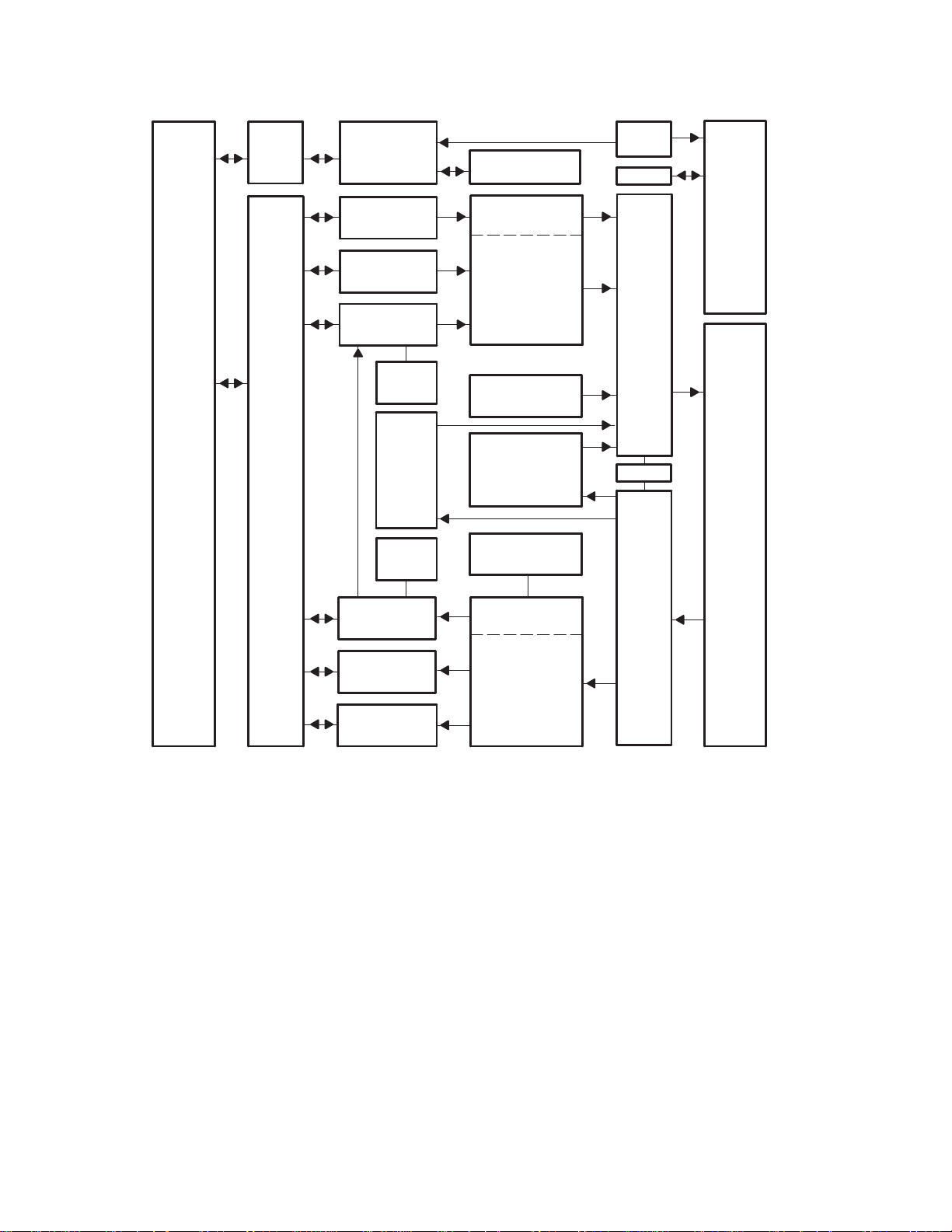
2 Terminal Descriptions
This section provides the terminal descriptions for the TSB12LV26. Figure 2–1 shows the signal assigned to each
terminal in the package. Table 2–1 is a listing of signal names arranged in terminal number order, and Table 2–2 lists
terminals in alphanumeric order by signal names.
PZ PACKAGE
(TOP VIEW)
GND
GPIO2
GPIO3
SCL
SDA
V
CCP
PCI_CLKRUN
PCI_INTA
3.3 V
CC
G_RST
GND
PCI_CLK
3.3 V
CC
PCI_GNT
PCI_REQ
V
CCP
PCI_PME
PCI_AD31
PCI_AD30
3.3 V
CC
PCI_AD29
PCI_AD28
PCI_AD27
GND
PCI_AD26
1
2
3
4
5
6
7
8
9
10
11
12
13
14
15
16
17
18
19
20
21
22
23
24
25
REG18
PHY_LPS
PHY_LINKON
98
99
100
28
27
26
CC
PHY_SCLK
3.3 V
95
96
31
30
GND
94
32
PHY_LREQ
97
29
CC
PHY_CTL1
PHY_CTL0
93
33
92
34
PHY_DATA0
3.3 V
90
91
36
35
PHY_DATA1
89
37
PHY_DATA2
88
38
CCP
V
87
39
PHY_DATA3
86
40
CC
PHY_DATA6
44
82
PHY_DATA7
81
45
3.3 V
REG_EN
79
80
47
46
PCI_RST
CYCLEOUT
CYCLEIN
76
77
78
75
74
73
72
71
70
69
68
67
66
65
64
63
62
61
60
59
58
57
56
55
54
53
52
51
50
49
48
GND
PCI_AD0
PCI_AD1
PCI_AD2
PCI_AD3
3.3 V
CC
PCI_AD4
PCI_AD5
PCI_AD6
PCI_AD7
PCI_C/BE0
PCI_AD8
V
CCP
PCI_AD9
PCI_AD10
GND
PCI_AD11
PCI_AD12
PCI_AD13
PCI_AD14
3.3 V
CC
PCI_AD15
PCI_C/BE1
PCI_P AR
PCI_SERR
PHY_DATA5
GND
PHY_DATA4
83
84
85
43
42
41
GND
CC
3.3 V
PCI_AD25
PCI_AD24
PCI_C/BE3
PCI_IDSEL
PCI_AD23
PCI_AD20
PCI_AD21
PCI_AD19
PCI_AD18
PCI_AD22
Figure 2–1. Terminal Assignments
CCP
V
PCI_AD17
PCI_AD16
PCI_C/BE2
REG18
PCI_IRDY
PCI_FRAME
CC
3.3 V
PCI_TRDY
PCI_STOP
PCI_DEVSEL
GND
PCI_PERR
2–1
Page 14

Table 2–1. Signals Sorted by Terminal Number
NO. TERMINAL NAME NO. TERMINAL NAME NO. TERMINAL NAME NO. TERMINAL NAME
1 GND 26 PCI_AD25 51 PCI_SERR 76 PCI_RST
2 GPIO2 27 PCI_AD24 52 PCI_PAR 77 CYCLEOUT
3 GPIO3 28 PCI_C/BE3 53 PCI_C/BE1 78 CYCLEIN
4 SCL 29 PCI_IDSEL 54 PCI_AD15 79 REG_EN
5 SDA 30 GND 55 3.3 V
6 V
7 PCI_CLKRUN 32 PCI_AD22 57 PCI_AD13 82 PHY_DATA6
8 PCI_INTA 33 PCI_AD21 58 PCI_AD12 83 GND
9 3.3 V
10 G_RST 35 3.3 V
11 GND 36 PCI_AD19 61 PCI_AD10 86 PHY_DATA3
12 PCI_CLK 37 PCI_AD18 62 PCI_AD9 87 V
13 3.3 V
14 PCI_GNT 39 V
15 PCI_REQ 40 PCI_AD16 65 PCI_C/BE0 90 PHY_DATA0
16 V
17 PCI_PME 42 REG18 67 PCI_AD6 92 PHY_CTL1
18 PCI_AD31 43 PCI_FRAME 68 PCI_AD5 93 PHY_CTL0
19 PCI_AD30 44 PCI_IRDY 69 PCI_AD4 94 GND
20 3.3 V
21 PCI_AD29 46 3.3 V
22 PCI_AD28 47 PCI_DEVSEL 72 PCI_AD2 97 PHY_LREQ
23 PCI_AD27 48 PCI_STOP 73 PCI_AD1 98 PHY_LINKON
24 GND 49 PCI_PERR 74 PCI_AD0 99 PHY_LPS
25 PCI_AD26 50 GND 75 GND 100 REG18
CCP
CC
CC
CCP
CC
31 PCI_AD23 56 PCI_AD14 81 PHY_DATA7
34 PCI_AD20 59 PCI_AD1 1 84 PHY_DATA5
CC
38 PCI_AD17 63 V
CCP
41 PCI_C/BE2 66 PCI_AD7 91 3.3 V
45 PCI_TRDY 70 3.3 V
CC
60 GND 85 PHY_DATA4
64 PCI_AD8 89 PHY_DATA1
71 PCI_AD3 96 3.3 V
CC
CCP
CC
80 3.3 V
88 PHY_DATA2
95 PHY_SCLK
CC
CCP
CC
CC
2–2
Page 15

Table 2–2. Signal Names Sorted Alphanumerically to T erminal Number
I/O
DESCRIPTION
TERMINAL NAME NO. TERMINAL NAME NO. TERMINAL NAME NO. TERMINAL NAME NO.
CYCLEIN 78 PCI_AD11 59 PCI_CLK 12 PHY_DATA7 81
CYCLEOUT 77 PCI_AD12 58 PCI_CLKRUN 7 PHY_LINKON 98
GND 1 PCI_AD13 57 PCI_DEVSEL 47 PHY_LPS 99
GND 11 PCI_AD14 56 PCI_FRAME 43 PHY_LREQ 97
GND 24 PCI_AD15 54 PCI_GNT 14 PHY_SCLK 95
GND 30 PCI_AD16 40 PCI_IDSEL 29 REG_EN 79
GND 50 PCI_AD17 38 PCI_INTA 8 REG18 42
GND 60 PCI_AD18 37 PCI_IRDY 44 REG18 100
GND 75 PCI_AD19 36 PCI_PAR 52 SCL 4
GND 83 PCI_AD20 34 PCI_PERR 49 SDA 5
GND 94 PCI_AD21 33 PCI_PME 17 V
GPIO2 2 PCI_AD22 32 PCI_REQ 15 V
GPIO3 3 PCI_AD23 31 PCI_RST 76 V
G_RST 10 PCI_AD24 27 PCI_SERR 51 V
PCI_AD0 74 PCI_AD25 26 PCI_STOP 48 V
PCI_AD1 73 PCI_AD26 25 PCI_TRDY 45 3.3 V
PCI_AD2 72 PCI_AD27 23 PHY_CTL0 93 3.3 V
PCI_AD3 71 PCI_AD28 22 PHY_CTL1 92 3.3 V
PCI_AD4 69 PCI_AD29 21 PHY_DAT A0 90 3.3 V
PCI_AD5 68 PCI_AD30 19 PHY_DAT A1 89 3.3 V
PCI_AD6 67 PCI_AD31 18 PHY_DAT A2 88 3.3 V
PCI_AD7 66 PCI_C/BE0 65 PHY_DATA3 86 3.3 V
PCI_AD8 64 PCI_C/BE1 53 PHY_DATA4 85 3.3 V
PCI_AD9 62 PCI_C/BE2 41 PHY_DATA5 84 3.3 V
PCI_AD10 61 PCI_C/BE3 28 PHY_DATA6 82 3.3 V
CCP
CCP
CCP
CCP
CCP
CC
CC
CC
CC
CC
CC
CC
CC
CC
CC
6
16
39
63
87
9
13
20
35
46
55
70
80
91
96
The terminals in Table 2–3 through Table 2–8 are grouped in tables by functionality, such as PCI system function
and power supply function. The terminal numbers are also listed for convenient reference.
Table 2–3. Power Supply Terminals
TERMINAL
NAME NO.
1, 11, 24, 30,
CC
50, 60, 75, 83,
94
6, 16, 39, 63,
87
9, 13, 20, 35,
46, 55, 70, 80,
91, 96
I Device ground terminals
I PCI signaling clamp voltage power input. PCI signals are clamped per the
I 3.3-V power supply terminals
PCI Local Bus Specification
.
GND
V
CCP
3.3 V
2–3
Page 16
TERMINAL
I/O
DESCRIPTION
NAME NO.
G_RST 10 I
PCI_CLK 12 I
PCI_INTA 8 O
PCI_RST 76 I
Table 2–4. PCI System Terminals
Global power reset. This reset brings all of the TSB12L V26 internal registers to their default states, including
those registers not reset by PCI_RST
When implementing wake capabilities from the 1394 host controller, it is necessary to implement two resets
to the TSB12LV26. G_RST
PCI bus RST
PCI_RST
PCI bus clock. Provides timing for all transactions on the PCI bus. All PCI signals are sampled at rising edge
of PCI_CLK.
Interrupt signal. This output indicates interrupts from the TSB12L V26 to the host. This terminal is implemented
as open-drain.
PCI reset. When this bus reset is asserted, the TSB12L V26 places all output buffers in a high impedance state
and resets all internal registers except device power management context- and vendor-specific bits initialized
by host power-on software. When PCI_RST
If this terminal is implemented, then it should be connected to the PCI bus RST
be pulled high to link VCC through a 4.7-kΩ resistor, or strapped to the G_RST
10).
. If wake capabilities are not required, G_RST may be connected to the PCI bus RST (see
, terminal 76).
should be a one-time power-on reset, and PCI_RST should be connected to the
. When G_RST is asserted, the device is completely nonfunctional.
is asserted, the device is completely nonfunctional.
signal. Otherwise, it should
terminal (see G_RST , terminal
2–4
Page 17

TERMINAL
I/O
DESCRIPTION
NAME NO.
PCI_AD31
PCI_AD30
PCI_AD29
PCI_AD28
PCI_AD27
PCI_AD26
PCI_AD25
PCI_AD24
PCI_AD23
PCI_AD22
PCI_AD21
PCI_AD20
PCI_AD19
PCI_AD18
PCI_AD17
PCI_AD16
PCI_AD15
PCI_AD14
PCI_AD13
PCI_AD12
PCI_AD11
PCI_AD10
PCI_AD9
PCI_AD8
PCI_AD7
PCI_AD6
PCI_AD5
PCI_AD4
PCI_AD3
PCI_AD2
PCI_AD1
PCI_AD0
18
19
21
22
23
25
26
27
31
32
33
34
36
37
38
40
54
56
57
58
59
61
62
64
66
67
68
69
71
72
73
74
Table 2–5. PCI Address and Data Terminals
PCI address/data bus. These signals make up the multiplexed PCI address and data bus on the PCI interface.
During the address phase of a PCI cycle, AD31–AD0 contain a 32-bit address or other destination information.
I/O
During the data phase, AD31–AD0 contain data.
2–5
Page 18

Table 2–6. PCI Interface Control Terminals
I/O
DESCRIPTION
TERMINAL
NAME NO.
PCI_C/BE0
PCI_C/BE1
PCI_C/BE2
PCI_C/BE3
PCI_CLKRUN 7 I/O
PCI_DEVSEL 47 I/O
PCI_FRAME 43 I/O
PCI_GNT 14 I
PCI_IDSEL 29 I
PCI_IRDY 44 I/O
PCI_PAR 52 I/O
PCI_PERR 49 I/O
PCI_PME 17 O Power management event. This terminal indicates wake events to the host.
PCI_REQ 15 O
PCI_SERR 51 O
PCI_STOP 48 I/O
PCI_TRDY 45 I/O
65
53
41
28
PCI bus commands and byte enables. The command and byte enable signals are multiplexed on the same PCI
terminals. During the address phase of a bus cycle PCI_C/BE3
I/O
the data phase, this 4-bit bus is used as byte enables.
Clock run. This terminal provides clock control through the PCI_CLKRUN protocol. An internal pulldown
resistor is implemented on this terminal.
This terminal is implemented as open-drain.
PCI device select. The TSB12LV26 asserts this signal to claim a PCI cycle as the target device. As a PCI
initiator, the TSB12LV26 monitors this signal until a target responds. If no target responds before time-out
occurs, then the TSB12LV26 terminates the cycle with an initiator abort.
PCI cycle frame. This signal is driven by the initiator of a PCI bus cycle. PCI_FRAME is asserted to indicate
that a bus transaction is beginning, and data transfers continue while this signal is asserted. When PCI_FRAME
is deasserted, the PCI bus transaction is in the final data phase.
PCI bus grant. This signal is driven by the PCI bus arbiter to grant the TSB12LV26 access to the PCI bus after
the current data transaction has completed. This signal may or may not follow a PCI bus request, depending
upon the PCI bus parking algorithm.
Initialization device select. IDSEL selects the TSB12L V26 during configuration space accesses. IDSEL can be
connected to one of the upper 24 PCI address lines on the PCI bus.
PCI initiator ready. IRDY indicates the ability of the PCI bus initiator to complete the current data phase of the
transaction. A data phase is completed upon a rising edge of PCLK where both PCI_IRDY
asserted.
PCI parity. In all PCI bus read and write cycles, the TSB12L V26 calculates even parity across the AD and C/BE
buses. As an initiator during PCI cycles, the TSB12LV26 outputs this parity indicator with a one PCI_CLK delay .
As a target during PCI cycles, the calculated parity is compared to the initiator parity indicator; a miscompare
can result in a parity error assertion (PCI_PERR
PCI parity error indicator. This signal is driven by a PCI device to indicate that calculated parity does not match
PCI_PAR when PERR_ENB (bit 6) is set in the PCI command register (offset 04h, see Section 3.4).
PCI bus request. Asserted by the TSB12LV26 to request access to the bus as an initiator. The host arbiter
asserts the PCI_GNT
PCI system error. When SERR_ENB (bit 8) in the PCI command register (offset 04h, see Section 3.4) is set
the output is pulsed, indicating an address parity error has occurred. The TSB12LV26 needs not be the target
of the PCI cycle to assert this signal.
This terminal is implemented as open-drain.
PCI cycle stop signal. This signal is driven by a PCI target to request the initiator to stop the current PCI bus
transaction. This signal is used for target disconnects, and is commonly asserted by target devices which do
not support burst data transfers.
PCI target ready. PCI_TRDY indicates the ability of the PCI bus targer to complete the current data phase of
the transaction. A data phase is completed upon a rising edge of PCI_CLK where both PCI_IRDY
PCI_TRDY
are asserted.
signal when the TSB12LV26 has been granted access to the bus.
).
–PCI_C/BE0 defines the bus command. During
and PCI_TRDY are
and
2–6
Page 19

Table 2–7. IEEE 1394 PHY/Link Terminals
I/O
DESCRIPTION
I/O
DESCRIPTION
TERMINAL
NAME NO.
PHY_CTL1
PHY_CTL0
PHY_DATA7
PHY_DATA6
PHY_DATA5
PHY_DATA4
PHY_DATA3
PHY_DATA2
PHY_DATA1
PHY_DATA0
PHY_LINKON 98 I/O
PHY_LPS 99 I/O
PHY_LREQ 97 O Link request. This signal is driven by the TSB12L V26 to initiate a request for the PHY to perform some service.
PHY_SCLK 95 I System clock. This input from the PHY provides a 49.152-MHz clock signal for data synchronization.
92
93
81
82
84
85
86
88
89
90
PHY -link interface control. These bidirectional signals control passage of information between the two devices.
The TSB12LV26 can only drive these terminals after the PHY has granted permission following a link request
I/O
(PHY_LREQ).
PHY -link interface data. These bidirectional signals pass data between the TSB12LV26 and the PHY device.
These terminals are driven by the TSB12LV26 on transmissions and are driven by the PHY on reception. Only
I/O
PHY_DATA1–PHY_DATA0 are valid for 100-Mbit speeds, PHY_DATA3–PHY_DATA0 are valid for 200-Mbit
speeds, and PHY_DATA7–PHY_DATA0 are valid for 400-Mbit speeds.
LinkOn wake indication. The PHY_LINKON signal is pulsed by the PHY to activate the link, and 3.3-V signaling
is required.
When connected to the TSB41LV0X C/LKON terminal, a 1-kΩ series resistor is required between the link and
PHY .
Link power status. The PHY_LPS signal is asserted when the link is powered on, and 3.3-V signaling is
required.
Table 2–8. Miscellaneous Terminals
TERMINAL
NAME NO.
CYCLEOUT 77 I/O This terminal provides an 8-kHz cycle timer synchronization signal.
The CYCLEIN terminal allows an external 8-kHz clock to be used as a cycle timer for synchronization with other
CYCLEIN 78 I/O
GPIO2 2 I/O
GPIO3 3 I/O
REG_EN 79 I Regulator enable. This terminal is pulled low to ground through a 220-Ω resistor.
REG18
SCL 4 I/O
SDA 5 I/O
42
100
system devices.
If this terminal is not implemented, then it should be pulled high to the link VCC through a 4.7-kΩ resistor.
General-purpose I/O [2]. This terminal defaults as an input and if it is not implemented, then it is recommended
that it be pulled low to ground with a 220-Ω resistor.
General-purpose I/O [3]. This terminal defaults as an input and if it is not implemented, then it is recommended
that it be pulled low to ground with a 220-Ω resistor.
The REG18 terminals are connected to a 0.01 µF capacitor which, in turn, is connected to ground. The
I
capacitor provides a local bypass for the internal core voltage.
Serial clock. The TSB12LV26 determines whether a two-wire serial ROM is implemented at reset. If a two-wire
serial ROM is implemented, then this terminal provides the SCL serial clock signaling.
This terminal is implemented as open-drain, and for normal operation (a ROM is implemented in the design),
this terminal should be pulled high to the ROM VCC with a 2.7-kΩ resistor. Otherwise, it should be pulled low
to ground with a 220-Ω resistor.
Serial data. The TSB12LV26 determines whether a two-wire serial ROM is implemented at reset. If a two-wire
serial ROM is detected, then this terminal provides the SDA serial data signaling. This terminal must be wired
low to indicate no serial ROM is present.
This terminal is implemented as open-drain, and for normal operation (a ROM is implemented in the design),
this terminal should be pulled high to the ROM VCC with a 2.7-kΩ resistor. Otherwise, it should be pulled low
to ground with a 220-Ω resistor.
2–7
Page 20

2–8
Page 21

3 TSB12LV26 Controller Programming Model
This section describes the internal registers used to program the TSB12L V26. All registers are detailed in the same
format: a brief description for each register, followed by the register offset and a bit table describing the reset state
for each register.
A bit description table, typically included when the register contains bits of more than one type or purpose, indicates
bit field names, field access tags which appear in the
describes the field access tags.
Table 3–1. Bit Field Access Tag Descriptions
ACCESS TAG NAME MEANING
R Read Field may be read by software.
W Write Field may be written by software to any value.
S Set Field may be set by a write of 1. Writes of 0 have no effect.
C Clear Field may be cleared by a write of 1. Writes of 0 have no effect.
U Update Field may be autonomously updated by the TSB12LV26.
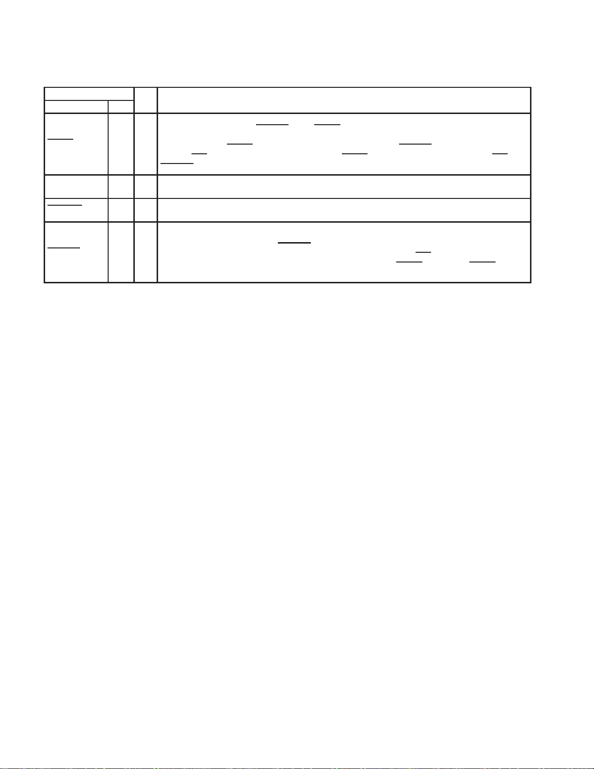
A simplified block diagram of the TSB12LV26 is provided in Figure 3–1.
type
column,and a detailed field description. Table 3–1
3–1
Page 22
PCI
Target
SM
Internal
Registers
OHCI PCI Power
Mgmt & CLKRUN
Serial
ROM
GPIOs
PCI
Host
Bus
Interface
Central
Arbiter
&
PCI
Initiator
SM
ISO Transmit
Contexts
Async Transmit
Contexts
Physical DMA
& Response
Resp
Timeout
PHY
Register
Access
& Status
Monitor
Request
Filters
General
Request Receive
Transmit
FIFO
Receive
Acknowledge
Cycle Start
Generator &
Cycle Monitor
Synthesized
Bus Reset
MISC
Interface
Link
Transmit
CRC
PHY /
Link
Interface
Link
Receive
Async Response
Receive
ISO Receive
Contexts
Receive
FIFO
Figure 3–1. TSB12LV26 Block Diagram
3–2
Page 23
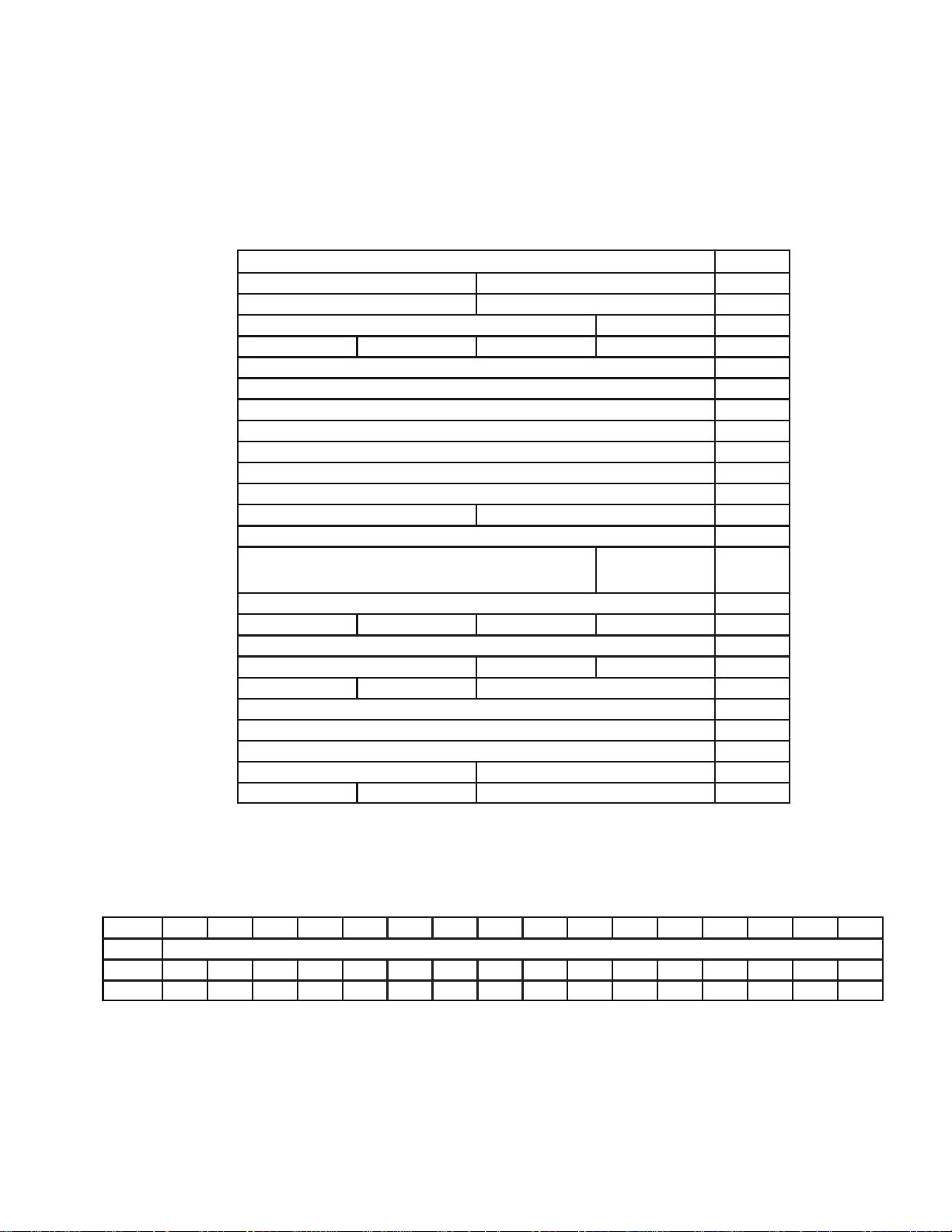
3.1 PCI Configuration Registers
The TSB12LV26 is a single-function PCI device. The configuration header is compliant with the
Specification
as a standard header. Table 3–2 illustrates the PCI configuration header that includes both the
predefined portion of the configuration space and the user definable registers.
Table 3–2. PCI Configuration Register Map
REGISTER NAME OFFSET
Device ID Vendor ID 00h
Status Command 04h
Class code Revision ID 08h
BIST Header type Latency timer Cache line size 0Ch
OHCI registers base address 10h
TI extension registers base address 14h
Reserved 18h
Reserved 1Ch
Reserved 20h
Reserved 24h
Reserved 28h
Subsystem ID Subsystem vendor ID 2Ch
Reserved 30h
PCI power
Reserved
Reserved 38h
Maximum latency Minimum grant Interrupt pin Interrupt line 3Ch
PCI OHCI control register 40h
Power management capabilities Next item pointer Capability ID 44h
PM data PMCSR_BSE Power management CSR 48h
Reserved 4Ch–ECh
PCI miscellaneous configuration register F0h
Link_Enhancements register F4h
Subsystem ID alias Subsystem vendor ID alias F8h
GPIO3 GPIO2 Reserved FCh
management
capabilities pointer
34h
PCI Local Bus
3.2 Vendor ID Register
The vendor ID register contains a value allocated by the PCI SIG and identifies the manufacturer of the PCI device.
The vendor ID assigned to Texas Instruments is 104Ch.
Bit 15 14 13 12 11 10 9 8 7 6 5 4 3 2 1 0
Name Vendor ID
Type R R R R R R R R R R R R R R R R
Default 0 0 0 1 0 0 0 0 0 1 0 0 1 1 0 0
Register: Vendor ID
Type: Read-only
Offset: 00h
Default: 104Ch
3–3
Page 24

3.3 Device ID Register
The device ID register contains a value assigned to the TSB12L V26 by Texas Instruments. The device identification
for the TSB12LV26 is 8020h.
Bit 15 14 13 12 11 10 9 8 7 6 5 4 3 2 1 0
Name Device ID
Type R R R R R R R R R R R R R R R R
Default 1 0 0 0 0 0 0 0 0 0 1 0 0 0 0 0
Register: Device ID
Type: Read-only
Offset: 02h
Default: 8020h
3.4 Command Register
The command register provides control over the TSB12L V26 interface to the PCI bus. All bit functions adhere to the
definitions in the
Bit 15 14 13 12 11 10 9 8 7 6 5 4 3 2 1 0
Name Command
Type R R R R R R R R/W R R/W R R/W R R/W R/W R
Default 0 0 0 0 0 0 0 0 0 0 0 0 0 0 0 0
PCI Local Bus Specification
, as seen in the bit descriptions of Table 3–3.
Register: Command
Type: Read/Write, Read-only
Offset: 04h
Default: 0000h
T able 3–3. Command Register Description
BIT FIELD NAME TYPE DESCRIPTION
15–10 RSVD R Reserved. Bits 15–10 return 0s when read.
9 FBB_ENB R
8 SERR_ENB R/W
7 STEP_ENB R
6 PERR_ENB R/W
5 VGA_ENB R
4 MWI_ENB R/W
3 SPECIAL R
2 MASTER_ENB R/W Bus master enable. When this bit is set, the TSB12LV26 is enabled to initiate cycles on the PCI bus.
1 MEMORY_ENB R/W
0 IO_ENB R
Fast back-to-back enable. The TSB12LV26 does not generate fast back-to-back transactions, thus
this bit returns 0 when read.
PCI_SERR enable. When this bit is set, the TSB12LV26 PCI_SERR driver is enabled. PCI_SERR can
be asserted after detecting an address parity error on the PCI bus.
Address/data stepping control. The TSB12L V26 does not support address/data stepping, thus this bit
is hardwired to 0.
Parity error enable. When this bit is set, the TSB12LV26 is enabled to drive PCI_PERR response to
parity errors through the PCI_PERR
VGA palette snoop enable. The TSB12LV26 does not feature VGA palette snooping. This bit returns 0
when read.
Memory write and invalidate enable. When this bit is set, the TSB12LV26 is enabled to generate MWI
PCI bus commands. If this bit is cleared, then the TSB12LV26 generates memory write commands
instead.
Special cycle enable. The TSB12LV26 function does not respond to special cycle transactions. This bit
returns 0 when read.
Memory response enable. Setting this bit enables the TSB12LV26 to respond to memory cycles on the
PCI bus. This bit must be set to access OHCI registers.
I/O space enable. The TSB12LV26 does not implement any I/O mapped functionality; thus, this bit returns 0 when read.
signal.
3–4
Page 25

3.5 Status Register
The status register provides status over the TSB12LV26 interface to the PCI bus. All bit functions adhere to the
definitions in the
Bit 15 14 13 12 11 10 9 8 7 6 5 4 3 2 1 0
Name Status
Type RCU RCU RCU RCU RCU R R RCU R R R R R R R R
Default 0 0 0 0 0 0 1 0 0 0 0 1 0 0 0 0
Register: Status
Type: Read/Clear/Update, Read-only
Offset: 06h
Default: 0210h
BIT FIELD NAME TYPE DESCRIPTION
15 PAR_ERR RCU Detected parity error. This bit is set when a parity error is detected, either address or data parity errors.
14 SYS_ERR RCU
13 MABORT RCU
12 TABORT_REC RCU
11 TABORT_SIG RCU
10–9 PCI_SPEED R
8 DATAPAR RCU
7 FBB_CAP R
6 UDF R
5 66MHZ R
4 CAPLIST R
3–0 RSVD R Reserved. Bits 3–0 return 0s when read.
PCI Local Bus Specification
Table 3–4. Status Register Description
Signaled system error. This bit is set when PCI_SERR is enabled and the TSB12L V26 has signaled a
system error to the host.
Received master abort. This bit is set when a cycle initiated by the TSB12LV26 on the PCI bus has been
terminated by a master abort.
Received target abort. This bit is set when a cycle initiated by the TSB12LV26 on the PCI bus was
terminated by a target abort.
Signaled target abort. This bit is set by the TSB12L V26 when it terminates a transaction on the PCI bus
with a target abort.
DEVSEL timing. Bits 10–9 encode the timing of PCI_DEVSEL and are hardwired to 01b indicating that
the TSB12LV26 asserts this signal at a medium speed on nonconfiguration cycle accesses.
Data parity error detected. This bit is set when the following conditions have been met:
a. PCI_PERR
b. The TSB12LV26 was the bus master during the data parity error.
c. The parity error response bit is set in the PCI command register (offset 04h, see Section 3.4).
Fast back-to-back capable. The TSB12LV26 cannot accept fast back-to-back transactions; thus, this
bit is hardwired to 0.
User definable features (UDF) supported. The TSB12L V26 does not support the UDF; thus, this bit is
hardwired to 0.
66-MHz capable. The TSB12L V26 operates at a maximum PCI_CLK frequency of 33 MHz; therefore,
this bit is hardwired to 0.
Capabilities list. This bit returns 1 when read, indicating that capabilities additional to standard PCI are
implemented. The linked list of PCI power management capabilities is implemented in this function.
. See Table 3–4 for a complete description of the register contents.
was asserted by any PCI device including the TSB12LV26.
3–5
Page 26

3.6 Class Code and Revision ID Register
The class code and revision ID register categorizes the TSB12L V26 as a serial bus controller (0Ch), controlling an
IEEE 1394 bus (00h), with an OHCI programming model (10h). Furthermore, the TI chip revision is indicated in the
least significant byte. See Table 3–5 for a complete description of the register contents.
Bit 31 30 29 28 27 26 25 24 23 22 21 20 19 18 17 16
Name Class code and revision ID
Type R R R R R R R R R R R R R R R R
Default 0 0 0 0 1 1 0 0 0 0 0 0 0 0 0 0
Bit 15 14 13 12 11 10 9 8 7 6 5 4 3 2 1 0
Name Class code and revision ID
Type R R R R R R R R R R R R R R R R
Default 0 0 0 1 0 0 0 0 0 0 0 0 0 0 0 0
Register: Class code and revision ID
Type: Read-only
Offset: 08h
Default: 0C00 1000h
Table 3–5. Class Code and Revision ID Register Description
BIT FIELD NAME TYPE DESCRIPTION
31–24 BASECLASS R
23–16 SUBCLASS R
15–8 PGMIF R
7–0 CHIPREV R Silicon revision. This field returns 00h when read, indicating the silicon revision of the TSB12LV26.
Base class. This field returns 0Ch when read, which broadly classifies the function as a serial bus
controller.
Subclass. This field returns 00h when read, which specifically classifies the function as controlling an
IEEE 1394 serial bus.
Programming interface. This field returns 10h when read, indicating that the programming model is
compliant with the
1394 Open Host Controller Interface Specification
.
3.7 Latency Timer and Class Cache Line Size Register
The latency timer and class cache line size register is programmed by host BIOS to indicate system cache line size
and the latency timer associated with the TSB12LV26. See Table 3–6 for a complete description of the register
contents.
Bit 15 14 13 12 11 10 9 8 7 6 5 4 3 2 1 0
Name Latency timer and class cache line size
Type R/W R/W R/W R/W R/W R/W R/W R/W R/W R/W R/W R/W R/W R/W R/W R/W
Default 0 0 0 0 0 0 0 0 0 0 0 0 0 0 0 0
Register: Latency timer and class cache line size
Type: Read/Write,
Offset: 0Ch
Default: 0000h
Table 3–6. Latency Timer and Class Cache Line Size Register Description
BIT FIELD NAME TYPE DESCRIPTION
PCI latency timer. The value in this register specifies the latency timer for the TSB12LV26, in units of
15–8 LATENCY_TIMER R/W
7–0 CACHELINE_SZ R/W
PCI clock cycles. When the TSB12LV26 is a PCI bus initiator and asserts PCI_FRAME
timer begins counting from zero. If the latency timer expires before the TSB12LV26 transaction has
terminated, then the TSB12LV26 terminates the transaction when its PCI_GNT
Cache line size. This value is used by the TSB12L V26 during memory write and invalidate, memory
read line, and memory read multiple transactions.
, the latency
is deasserted.
3–6
Page 27

3.8 Header Type and BIST Register
The header type and BIST register indicates the TSB12L V26 PCI header type, and indicates no built-in self test. See
Table 3–7 for a complete description of the register contents.
Bit 15 14 13 12 11 10 9 8 7 6 5 4 3 2 1 0
Name Header type and BIST
Type R R R R R R R R R R R R R R R R
Default 0 0 0 0 0 0 0 0 0 0 0 0 0 0 0 0
Register: Header type and BIST
Type: Read-only
Offset: 0Eh
Default: 0000h
Table 3–7. Header Type and BIST Register Description
BIT FIELD NAME TYPE DESCRIPTION
15–8 BIST R
7–0 HEADER_TYPE R
Built-in self test. The TSB12LV26 does not include a built-in self test; thus, this field returns 00h when
read.
PCI header type. The TSB12LV26 includes the standard PCI header, and this is communicated by
returning 00h when this field is read.
3.9 OHCI Base Address Register
The OHCI base address register is programmed with a base address referencing the memory-mapped OHCI control.
When BIOS writes all 1s to this register, the value read back is FFFF F800h, indicating that at least 2K bytes of
memory address space are required for the OHCI registers. See T able 3–8 for a complete description of the register
contents.
Bit 31 30 29 28 27 26 25 24 23 22 21 20 19 18 17 16
Name OHCI base address
Type R/W R/W R/W R/W R/W R/W R/W R/W R/W R/W R/W R/W R/W R/W R/W R/W
Default 0 0 0 0 0 0 0 0 0 0 0 0 0 0 0 0
Bit 15 14 13 12 11 10 9 8 7 6 5 4 3 2 1 0
Name OHCI address
Type R/W R/W R/W R/W R/W R R R R R R R R R R R
Default 0 0 0 0 0 0 0 0 0 0 0 0 0 0 0 0
Register: OHCI base address
Type: Read/Write, Read-only
Offset: 10h
Default: 0000 0000h
Table 3–8. OHCI Base Address Register Description
BIT FIELD NAME TYPE DESCRIPTION
31–1 1 OHCIREG_PTR R/W OHCI register pointer. Specifies the upper 21 bits of the 32-bit OHCI base address register.
10–4 OHCI_SZ R
3 OHCI_PF R
2–1 OHCI_MEMTYPE R
0 OHCI_MEM R
OHCI register size. This field returns 0s when read, indicating that the OHCI registers require a
2-Kbyte region of memory.
OHCI register prefetch. This bit returns 0 when read, indicating that the OHCI registers are
nonprefetchable.
OHCI memory type. This field returns 0s when read, indicating that the OHCI base address register is
32 bits wide and mapping can be done anywhere in the 32-bit memory space.
OHCI memory indicator. This bit returns 0 when read, indicating that the OHCI registers are mapped
into system memory space.
3–7
Page 28

3.10 TI Extension Base Address Register
The TI extension base address register is programmed with a base address referencing the memory-mapped TI
extension registers. See the
Bit 31 30 29 28 27 26 25 24 23 22 21 20 19 18 17 16
Name TI extension base address
Type R/W R/W R/W R/W R/W R/W R/W R/W R/W R/W R/W R/W R/W R/W R/W R/W
Default 0 0 0 0 0 0 0 0 0 0 0 0 0 0 0 0
Bit 15 14 13 12 11 10 9 8 7 6 5 4 3 2 1 0
Name TI extension base address
Type R/W R/W R/W R/W R/W R R R R R R R R R R R
Default 0 0 0 0 0 0 0 0 0 0 0 0 0 0 0 0
OHCI Base Address Register
, Section 3.9, for bit field details.
Register: TI extension base address
Type: Read/Write, Read-only
Offset: 14h
Default: 0000 0000h
3.11 Subsystem Identification Register
The subsystem identification register is used for system and option card identification purposes. This register can
be initialized from the serial ROM or programmed via the subsystem ID and subsystem vendor ID alias registers at
offset F8h. See Table 3–9 for a complete description of the register contents.
Bit 31 30 29 28 27 26 25 24 23 22 21 20 19 18 17 16
Name Subsystem identification
Type RU RU RU RU RU RU RU RU RU RU RU RU RU RU RU RU
Default 0 0 0 0 0 0 0 0 0 0 0 0 0 0 0 0
Bit 15 14 13 12 11 10 9 8 7 6 5 4 3 2 1 0
Name Subsystem identification
Type RU RU RU RU RU RU RU RU RU RU RU RU RU RU RU RU
Default 0 0 0 0 0 0 0 0 0 0 0 0 0 0 0 0
Register: Subsystem identification
Type: Read/Update
Offset: 2Ch
Default: 0000 0000h
Table 3–9. Subsystem Identification Register Description
BIT FIELD NAME TYPE DESCRIPTION
31–16 OHCI_SSID RU Subsystem device ID. This field indicates the subsystem device ID.
15–0 OHCI_SSVID RU Subsystem vendor ID. This field indicates the subsystem vendor ID.
3–8
Page 29

3.12 Power Management Capabilities Pointer Register
The power management capabilities pointer register provides a pointer into the PCI configuration header where the
PCI power management register block resides. The TSB12LV26 configuration header double-words at offsets 44h
and 48h provide the power management registers. This register is read-only and returns 44h when read.
Bit 7 6 5 4 3 2 1 0
Name Power management capabilities pointer
Type R R R R R R R R
Default 0 1 0 0 0 1 0 0
Register: Power management capabilities pointer
Type: Read-only
Offset: 34h
Default: 44h
3.13 Interrupt Line and Pin Register
The interrupt line and pin register is used to communicate interrupt line routing information. See Table 3–10 for a
complete description of the register contents.
Bit 15 14 13 12 11 10 9 8 7 6 5 4 3 2 1 0
Name Interrupt line and pin
Type R R R R R R R R R/W R/W R/W R/W R/W R/W R/W R/W
Default 0 0 0 0 0 0 0 1 0 0 0 0 0 0 0 0
Register: Interrupt line and pin
Type: Read/Write, Read-only
Offset: 3Ch
Default: 0100h
Table 3–10. Interrupt Line and Pin Register Description
BIT FIELD NAME TYPE DESCRIPTION
15–8 INTR_PIN R
7–0 INTR_LINE R/W
Interrupt pin. Returns 01h when read, indicating that the TSB12LV26 PCI function signals interrupts on
the PCI_INTA
Interrupt line. This field is programmed by the system and indicates to software which interrupt line the
TSB12L V26 PCI_INTA
pin.
is connected to.
3–9
Page 30

3.14 MIN_GNT and MAX_LAT Register
The MIN_GNT and MAX_LAT register is used to communicate to the system the desired setting of bits 15–8 of the
latency timer and class cache line size register (offset 0Ch, see Section 3.7). If a serial ROM is detected, then the
contents of this register are loaded through the serial ROM interface after a PCI reset. If no serial ROM is detected,
then this register returns a default value that corresponds to the MIN_GNT = 2, MAX_LAT = 4. See Table 3–11 for
a complete description of the register contents.
Bit 15 14 13 12 11 10 9 8 7 6 5 4 3 2 1 0
Name MIN_GNT and MAX_LAT
Type RU RU RU RU RU RU RU RU RU RU RU RU RU RU RU RU
Default 0 0 0 0 0 1 0 0 0 0 0 0 0 0 1 0
Register: MIN_GNT and MAX_LAT
Type: Read/Update
Offset: 3Eh
Default: 0402h
Table 3–11. MIN_GNT and MAX_LAT Register Description
BIT FIELD NAME TYPE DESCRIPTION
Maximum latency. The contents of this register may be used by host BIOS to assign an arbitration
15–8 MAX_LAT RU
7–0 MIN_GNT RU
priority-level to the TSB12LV26. The default for this register indicates that the TSB12LV26 may need to
access the PCI bus as often as every 0.25 µs; thus, an extremely high priority level is requested. The
contents of this field may also be loaded through the serial ROM.
Minimum grant. The contents of this register may be used by host BIOS to assign a latency timer and class
cache line size register (offset 0Ch, see Section 3.7) value to the TSB12L V26. The default for this register
indicates that the TSB12L V26 may need to sustain burst transfers for nearly 64 µs; thus, requesting a large
value be programmed in bits 15–8 of the TSB12LV26 latency timer and class cache line size register.
3.15 OHCI Control Register
The OHCI control register is defined by the
big endian PCI support. See Table 3–12 for a complete description of the register contents.
Bit 31 30 29 28 27 26 25 24 23 22 21 20 19 18 17 16
Name OHCI control
Type R R R R R R R R R R R R R R R R
Default 0 0 0 0 0 0 0 0 0 0 0 0 0 0 0 0
Bit 15 14 13 12 11 10 9 8 7 6 5 4 3 2 1 0
Name OHCI control
Type R R R R R R R R R R R R R R R R/W
Default 0 0 0 0 0 0 0 0 0 0 0 0 0 0 0 0
Register: OHCI control
Type: Read/Write
Offset: 40h
Default: 0000 0000h
Table 3–12. OHCI Control Register Description
BIT FIELD NAME TYPE DESCRIPTION
31–1 RSVD R Reserved. Bits 31–1 return 0s when read.
0 GLOBAL_SWAP R/W
When this bit is set, all quadlets read from and written to the PCI interface are byte swapped (big
endian). This bit is loaded from ROM and should be programmed to 0 for normal operation.
1394 Open Host Controller Interface Specification
and provides a bit for
3–10
Page 31

3.16 Capability ID and Next Item Pointer Register
The capability ID and next item pointer register identifies the linked list capability item and provides a pointer to the
next capability item. See Table 3–13 for a complete description of the register contents.
Bit 15 14 13 12 11 10 9 8 7 6 5 4 3 2 1 0
Name Capability ID and next item pointer
Type R R R R R R R R R R R R R R R R
Default 0 0 0 0 0 0 0 0 0 0 0 0 0 0 0 1
Register: Capability ID and next item pointer
Type: Read-only
Offset: 44h
Default: 0001h
Table 3–13. Capability ID and Next Item Pointer Register Description
BIT FIELD NAME TYPE DESCRIPTION
15–8 NEXT_ITEM R
7–0 CAPABILITY_ID R
Next item pointer. The TSB12LV26 supports only one additional capability that is communicated to
the system through the extended capabilities list; thus, this field returns 00h when read.
Capability identification. This field returns 01h when read, which is the unique ID assigned by the PCI
SIG for PCI power management capability.
3–11
Page 32

3.17 Power Management Capabilities Register
The power management capabilities register indicates the capabilities of the TSB12LV26 related to PCI power
management. See Table 3–14 for a complete description of the register contents.
Bit 15 14 13 12 11 10 9 8 7 6 5 4 3 2 1 0
Name Power management capabilities
Type RU RU RU RU RU RU R R R R R R R R R R
Default 0 1 1 0 0 1 0 0 0 0 0 0 0 0 0 1
Register: Power management capabilities
Type: Read/Update, Read-only
Offset: 46h
Default: 6401h
Table 3–14. Power Management Capabilities Register Description
BIT FIELD NAME TYPE DESCRIPTION
PCI_PME support from D3
15 PME_D3COLD RU
14–1 1 PME_SUPPORT RU
10 D2_SUPPORT RU
9 D1_SUPPORT R
8 DYN_DATA R
7–6 RSVD R Reserved. Bits 7–6 return 0s when read.
5 DSI R
4 AUX_PWR R
3 PME_CLK R
2–0 PM_VERSION R
from D3
configured by host software using bit 15 (PME_D3COLD) in the PCI miscellaneous configuration
register (see Section 3.20).
PCI_PME support. This 4-bit field indicates the power states from which the TSB12L V26 may assert
PCI_PME
from the D3
(PME_SUPPORT_D2) in the PCI miscellaneous configuration register (offset F0h, see Section 3.20).
D2 support. This bit can be set or cleared via bit 10 (D2_SUPPORT) in the PCI miscellaneous
configuration register (see Section 3.20). The PCI miscellaneous configuration register is loaded from
ROM. When this bit is set, it indicates that D2 support is present. When this bit is cleared, it indicates
that D2 support is not present for backward compatibility with the TSB12LV22. For normal operation,
this bit is set to 1.
D1 support. This bit returns a 0 when read, indicating that the TSB12LV26 does not support the D1
power state.
Dynamic data support. This bit returns a 0 when read, indicating that the TSB12LV26 does not report
dynamic power consumption data.
Device specific initialization. This bit returns 0 when read, indicating that the TSB12LV26 does not
require special initialization beyond the standard PCI configuration header before a generic class
driver is able to use it.
Auxiliary power source. Since the TSB12LV26 does not support PCI_PME generation in the D3
device state, this bit returns 0 when read.
PME clock. This bit returns 0 when read, indicating that no host bus clock is required for the
TSB12L V26 to generate PCI_PME
Power management version. This field returns 001b when read, indicating that the TSB12LV26 is
compatible with the registers described in the
Rev. 1.0
. This bit state is dependent upon the TSB12LV26 V
cold
. This field returns a value of 1100b by default, indicating that PCI_PME may be asserted
and D2 power states. Bit 13 may be modified by host software using bit 13
hot
.
. When this bit is set, the TSB12LV26 generates a PCI_PME wake event
cold
.
PCI Bus Power Management Interface Specification
implementation and may be
AUX
cold
3–12
Page 33

3.18 Power Management Control and Status Register
The power management control and status register implements the control and status of the PCI power management
function. This register is not affected by the internally generated reset caused by the transition from the D3
state. See Table 3–15 for a complete description of the register contents.
Bit 15 14 13 12 11 10 9 8 7 6 5 4 3 2 1 0
Name Power management control and status
Type RC R R R R R R R/W R R R R R R R/W R/W
Default 0 0 0 0 0 0 0 0 0 0 0 0 0 0 0 0
Register: Power management control and status
Type: Read/Clear, Read/Write, Read-only
Offset: 48h
Default: 0000h
Table 3–15. Power Management Control and Status Register Description
BIT FIELD NAME TYPE DESCRIPTION
This bit is set when the TSB12LV26 would normally be asserting the PME signal, independent of the
15 PME_STS RC
14–9 DYN_CTRL R
8 PME_ENB R/W
7–5 RSVD R Reserved. Bits 7–5 return 0s when read.
4 DYN_DATA R Dynamic data. This bit returns 0 when read since the TSB12LV26 does not report dynamic data.
3–2 RSVD R Reserved. Bits 3–2 return 0s when read.
1–0 PWR_STA TE R/W
state of bit 8 (PME_ENB). This bit is cleared by a writeback of 1, and this also clears the PCI_PME
signal driven by the TSB12LV26. Writing a 0 to this bit has no effect.
Dynamic data control. This field returns 0s when read since the TSB12LV26 does not report dynamic
data.
PCI_PME enable. This bit enables the function to assert PCI_PME. If this bit is cleared, then assertion
of PCI_PME
Power state. This 2-bit field is used to set the TSB12LV26 device power state and is encoded as
follows:
00 = Current power state is D0
01 = Current power state is D1
10 = Current power state is D2
11 = Current power state is D3
is disabled.
hot
to D0
3.19 Power Management Extension Register
The power management extension register provides extended power management features not applicable to the
TSB12L V26, thus it is read-only and returns 0s when read. See Table 3–16 for a complete description of the register
contents.
Bit 15 14 13 12 11 10 9 8 7 6 5 4 3 2 1 0
Name Power management extension
Type R R R R R R R R R R R R R R R R
Default 0 0 0 0 0 0 0 0 0 0 0 0 0 0 0 0
Register: Power management extension
Type: Read-only
Offset: 4Ah
Default: 0000h
Table 3–16. Power Management Extension Register Description
BIT FIELD NAME TYPE DESCRIPTION
15–8 PM_DATA R
7–0 PMCSR_BSE R
Power management data. This field returns 00h when read since the TSB12LV26 does not report
dynamic data.
Power management CSR – bridge support extensions. This field returns 00h when read since the
TSB12L V26 does not provide P2P bridging.
3–13
Page 34

3.20 Miscellaneous Configuration Register
The miscellaneous configuration register provides miscellaneous PCI-related configuration. See Table 3–17 for a
complete description of the register contents.
Bit 31 30 29 28 27 26 25 24 23 22 21 20 19 18 17 16
Name Miscellaneous configuration
Type R R R R R R R R R R R R R R R R
Default 0 0 0 0 0 0 0 0 0 0 0 0 0 0 0 0
Bit 15 14 13 12 11 10 9 8 7 6 5 4 3 2 1 0
Name Miscellaneous configuration
Type R/W R R/W R R R/W R R R R R R/W R/W R/W R/W R/W
Default 0 0 1 0 0 1 0 0 0 0 0 0 0 0 0 0
Register: Miscellaneous configuration
Type: Read/Write, Read-only
Offset: F0h
Default: 0000 2400h
Table 3–17. Miscellaneous Configuration Register
BIT FIELD NAME TYPE DESCRIPTION
31–16 RSVD R Reserved. Bits 31–16 return 0s when read.
15 PME_D3COLD R/W
14 RSVD R Reserved. Bit 14 returns 0 when read.
13 PME_SUPPORT_D2 R/W
12–1 1 RSVD R Reserved. Bits 12–11 return 0s when read.
10 D2_SUPPORT R/W
9–5 RSVD R Reserved. Bits 9–5 return 0s when read.
4 DIS_TGT_ABT R/W
3 GP2IIC R/W
2 DISABLE_SCLKGATE R/W
1 DISABLE_PCIGATE R/W
0 KEEP_PCLK R/W
PCI_PME support from D3
management capabilities register (offset 46h, see Section 3.17).
PCI_PME support. This bit is used to program bit 13 (PME_SUPPORT_D2) in the power
management capabilities register (offset 46h, see Section 3.17). If wake from the D2 power state
implemented in the TSB12L V26 is not desired, then this bit may be cleared to indicate to power
management software that wake-up from D2 is not supported.
D2 support. This bit is used to program bit 10 (D2_SUPPORT) in the power management
capabilities register (offset 46h, see Section 3.17). If the D2 power state implemented in the
TSB12L V26 is not desired, then this bit may be cleared to indicate to power management software
that D2 is not supported.
This bit defaults to 0, which provides OHCI-Lynx compatible target abort signaling. When this bit is
set to 1, it enables the no-target-abort mode, in which the TSB12LV26 returns indeterminate data
instead of signaling target abort.
The link is divided into the PCI_CLK and SCLK domains. If software tries to access registers in the
link that are not active because the SCLK is disabled, a target abort is issued by the link. On some
systems this can cause a problem resulting in a fatal system error. Enabling this bit allows the link
to respond to these types of requests by returning FFh.
It is recommended that this bit be set to 1.
When this bit is set to 1, the GPIO3 and GPIO2 signals are internally routed to the SCL and SDA,
respectively. The GPIO3 and GPIO2 terminals are also placed in a high impedance state.
When this bit is set to 1, the internal SCLK runs identically with the chip input. This bit is a test
feature only and should be cleared to 0 (all applications).
When this bit is set, the internal PCI clock runs identically with the chip input. This bit is a test
feature only and should be cleared to 0 (all applications).
When this bit is set to 1, the PCI clock is always kept running through the PCI_CLKRUN protocol.
When this bit is cleared, the PCI clock may be stopped using PCI_CLKRUN
. This bit is used to program bit 15 (PME_D3COLD) in the power
cold
.
3–14
Page 35

3.21 Link Enhancement Control Register
The link enhancement control register implements TI proprietary bits that are initialized by software or by a serial
ROM, if present. After these bits are set, their functionality is enabled only if bit 22 (aPhyEnhanceEnable) in the host
controller control register (OHCI offset 50h/54h, see Section 4.16) is set. See Table 3–18 for a complete description
of the register contents.
Bit 31 30 29 28 27 26 25 24 23 22 21 20 19 18 17 16
Name Link enhancement control
Type R R R R R R R R R R R R R R R R
Default 0 0 0 0 0 0 0 0 0 0 0 0 0 0 0 0
Bit 15 14 13 12 11 10 9 8 7 6 5 4 3 2 1 0
Name Link enhancement control
Type R R R/W R/W R R R R R/W R R R R R/W R/W R
Default 0 0 0 1 0 0 0 0 0 0 0 0 0 0 0 0
Register: Link enhancement control
Type: Read/Write, Read-only
Offset: F4h
Default: 0000 1000h
Table 3–18. Link Enhancement Control Register Description
BIT FIELD NAME TYPE DESCRIPTION
31–14 RSVD R Reserved. Bits 31–14 return 0s when read.
This field sets the initial AT threshold value, which is used until the AT FIFO is underrun. When the
TSB12L V26 retries the packet, it uses a 2-Kbyte threshold resulting in a store-and-forward operation.
00 = Threshold ~ 2K bytes resulting in a store-and-forward operation
01 = Threshold ~ 1.7K bytes (default)
10 = Threshold ~ 1K bytes
11 = Threshold ~ 512 bytes
These bits fine-tune the asynchronous transmit threshold. For most applications the 1.7K threshold
is optimal. Changing this value may increase or decrease the 1394 latency depending on the average
13–12 atx_thresh R/W
11–8 RSVD R Reserved. Bits 11–8 return 0s when read.
7 enab_unfair R/W
6 RSVD R
5–3 RSVD R Reserved. Bits 5–3 return 0s when read.
2 enab_insert_idle R/W
PCI bus latency.
Setting the AT threshold to 1.7K, 1K, or 512 bytes results in data being transmitted at these thresholds,
or when an entire packet has been checked into the FIFO. If the packet to be transmitted is larger than
the AT threshold, then the remaning data must be received before the A T FIFO is emptied; otherwise,
an underrun condition will occur, resulting in a packet error at the receiving node. As a result, the link
will then commence store-and-forward operation, i.e., wait until it has the complete packet in the FIFO
before retransmitting it on the second attempt, to ensure delivery .
An AT threshold of 2K results in store-and-forward operation, which means that asynchronous data
will not be transmitted until an end-of-packet token is received. Restated, setting the AT threshold to
2K results in only complete packets being transmitted.
Enable asynchronous priority requests. OHCI-Lynx compatible. Setting this bit to 1 enables the link
to respond to requests with priority arbitration. It is recommended that this bit be set to 1.
This bit is not assigned in the TSB12LV26 follow-on products since this bit location loaded by the serial
ROM from the enhancements field corresponds to bit 23 (programPhyEnable) in the host controller
control register (OHCI offset 50h/54h, see Section 4.16).
Enable insert idle. OHCI-Lynx compatible. When the PHY has control of the Ct[0:1] control lines and
D[0:8] data lines and the link requests control, the PHY drives 11b on the Ct[0:1] lines. The link can
then start driving these lines immediately . Setting this bit to 1 inserts an idle state, so the link waits one
clock cycle before it starts driving the lines (turnaround time). It is recommended that this bit be set to
1.
3–15
Page 36

Table 3–18. Link Enhancement Control Register Description (Continued)
BIT FIELD NAME TYPE DESCRIPTION
Enable acceleration enhancements. OHCI-Lynx compatible. When set to 1, this bit notifies the PHY
1 enab_accel R/W
0 RSVD R Reserved. Bit 0 returns 0 when read.
that the link supports the 1394a acceleration enhancements, i.e., ack-accelerated, fly-by
concatenation, etc. It is recommended that this bit be set to 1.
3.22 Subsystem Access Register
Write access to the subsystem access register updates the subsystem identification registers identically to
OHCI-Lynx. The system ID value written to this register may also be read back from this register . See Table 3–19 for
a complete description of the register contents.
Bit 31 30 29 28 27 26 25 24 23 22 21 20 19 18 17 16
Name Subsystem access
Type R/W R/W R/W R/W R/W R/W R/W R/W R/W R/W R/W R/W R/W R/W R/W R/W
Default 0 0 0 0 0 0 0 0 0 0 0 0 0 0 0 0
Bit 15 14 13 12 11 10 9 8 7 6 5 4 3 2 1 0
Name Subsystem access
Type R/W R/W R/W R/W R/W R/W R/W R/W R/W R/W R/W R/W R/W R/W R/W R/W
Default 0 0 0 0 0 0 0 0 0 0 0 0 0 0 0 0
Register: Subsystem access
Type: Read/Write
Offset: F8h
Default: 0000 0000h
Table 3–19. Subsystem Access Register Description
BIT FIELD NAME TYPE DESCRIPTION
31–16 SUBDEV_ID R/W Subsystem device ID. This field indicates the subsystem device ID.
15–0 SUBVEN_ID R/W Subsystem vendor ID. This field indicates the subsystem vendor ID.
3–16
Page 37

3.23 GPIO Control Register
The GPIO control register has the control and status bits for the GPIO2 and GPIO3 ports. See Table 3–20 for a
complete description of the register contents.
Bit 31 30 29 28 27 26 25 24 23 22 21 20 19 18 17 16
Name GPIO control
Type R/W R R/W R/W R R R RWU R/W R R/W R/W R R R RWU
Default 0 0 0 0 0 0 0 0 0 0 0 0 0 0 0 0
Bit 15 14 13 12 11 10 9 8 7 6 5 4 3 2 1 0
Name GPIO control
Type R R R R R R R R R R R R R R R R
Default 0 0 0 0 0 0 0 0 0 0 0 0 0 0 0 0
Register: GPIO control
Type: Read/Write/Update, ReadWrite, Read-only
Offset: FCh
Default: 0000 0000h
Table 3–20. GPIO Control Register Description
BIT FIELD NAME TYPE DESCRIPTION
When this bit is set, a TSB12LV26 general-purpose interrupt event occurs on a level change of the
31 INT_3EN R/W
30 RSVD R Reserved. Bit 30 returns 0 when read.
29 GPIO_INV3 R/W GPIO3 polarity invert. When this bit is set, the polarity of GPIO3 is inverted.
28 GPIO_ENB3 R/W
27–25 RSVD R Reserved. Bits 27–25 return 0s when read.
24 GPIO_DATA3 RWU
23 INT_2EN R/W
22 RSVD R Reserved. Bit 22 returns 0 when read.
21 GPIO_INV2 R/W GPIO2 polarity invert. When this bit is set, the polarity of GPIO2 is inverted.
20 GPIO_ENB2 R/W
19–17 RSVD R Reserved. Bits 19–17 return 0s when read.
16 GPIO_DATA2 RWU
15–0 RSVD R Reserved. Bits 15–0 return 0s when read.
GPIO3 input. This event may generate an interrupt, with mask and event status reported through the
OHCI interrupt mask (OHCI offset 88h/8Ch, see Section 4.22) and interrupt event (OHCI offset
80h/84h, see Section 4.21) registers.
GPIO3 enable control. When this bit is set, the output is enabled. Otherwise, the output is high
impedance.
GPIO3 data. Reads from this bit return the logical value of the input to GPIO3. Writes to this bit update
the value to drive to GPIO3 when output is enabled.
When this bit is set, a TSB12LV26 general-purpose interrupt event occurs on a level change of the
GPIO2 input. This event may generate an interrupt, with mask and event status reported through the
OHCI interrupt mask (OHCI offset 88h/8Ch, see Section 4.22) and interrupt event (OHCI offset
80h/84h, see Section 4.21) registers.
GPIO2 enable control. When this bit is set, the output is enabled. Otherwise, the output is high
impedance.
GPIO2 data. Reads from this bit return the logical value of the input to GPIO2. Writes to this bit update
the value to drive to GPIO2 when the output is enabled.
3–17
Page 38

3–18
Page 39

4 OHCI Registers
Host controller control
The OHCI registers defined by the
1394 Open Host Controller Interface Specification
are memory-mapped into a
2-Kbyte region of memory pointed to by the OHCI base address register at offset 10h in PCI configuration space (see
Section 3.9). These registers are the primary interface for controlling the TSB12LV26 IEEE 1394 link function.
This section provides the register interface and bit descriptions. There are several set/clear register pairs in this
programming model, which are implemented to solve various issues with typical read-modify-write control registers.
There are two addresses for a set/clear register: RegisterSet and RegisterClear. Refer to Table 4–1 for an illustration.
A 1 bit written to RegisterSet causes the corresponding bit in the set/clear register to be set, while a 0 bit leaves the
corresponding bit unaffected. A 1 bit written to RegisterClear causes the corresponding bit in the set/clear register
to be cleared, while a 0 bit leaves the corresponding bit in the set/clear register unaffected.
Typically , a read from either RegisterSet or RegisterClear returns the contents of the set or clear register , respectively.
However, sometimes reading the RegisterClear provides a masked version of the set or clear register. The interrupt
event register is an example of this behavior.
Table 4–1. OHCI Register Map
DMA CONTEXT REGISTER NAME ABBREVIATION OFFSET
— OHCI version Version 00h
GUID ROM GUID_ROM 04h
Asynchronous transmit retries ATRetries 08h
CSR data CSRData 0Ch
CSR compare data CSRCompareData 10h
CSR control CSRControl 14h
Configuration ROM header ConfigROMhdr 18h
Bus identification BusID 1Ch
Bus options BusOptions 20h
GUID high GUIDHi 24h
GUID low GUIDLo 28h
Reserved — 2Ch–30h
Configuration ROM map ConfigROMmap 34h
Posted write address low PostedWriteAddressLo 38h
Posted write address high PostedWriteAddressHi 3Ch
Vendor identification VendorID 40h–4Ch
HCControlSet 50h
HCControlClr 54h
Reserved — 58h–5Ch
4–1
Page 40

Table 4–1. OHCI Register Map (Continued)
Isochronous receive channel mask high
Isochronous receive channel mask lo
Interrupt event
Interrupt mask
Isochronous transmit interrupt event
Isochronous transmit interrupt mask
Isochronous receive interrupt event
Isochronous receive interrupt mask
Link control
Asynchronous request filter high
Asynchronous request filter lo
Physical request filter high
Physical request filter lo
DMA CONTEXT REGISTER NAME ABBREVIATION OFFSET
Self ID Reserved — 60h
Self ID buffer SelfIDBuffer 64h
Self ID count SelfIDCount 68h
Reserved — 6Ch
—
p
p
p
p
—
Reserved B0–D8h
Fairness control FairnessControl DCh
Node identification NodeID E8h
PHY layer control PhyControl ECh
Isochronous cycle timer Isocyctimer F0h
Reserved F4h–FCh
Physical upper bound PhysicalUpperBound 120h
Reserved — 124h–17Ch
p
p
w
w
IRChannelMaskHiSet 70h
IRChannelMaskHiClear 74h
IRChannelMaskLoSet 78h
w
IRChannelMaskLoClear 7Ch
IntEventSet 80h
IntEventClear 84h
IntMaskSet 88h
IntMaskClear 8Ch
IsoXmitIntEventSet 90h
IsoXmitIntEventClear 94h
IsoXmitIntMaskSet 98h
IsoXmitIntMaskClear 9Ch
IsoRecvIntEventSet A0h
IsoRecvIntEventClear A4h
IsoRecvIntMaskSet A8h
IsoRecvIntMaskClear ACh
LinkControlSet E0h
LinkControlClear E4h
AsyncRequestFilterHiSet 100h
AsyncRequestFilterHiClear 104h
AsyncRequestFilterLoSet 108h
AsyncRequestFilterloClear 10Ch
PhysicalRequestFilterHiSet 110h
PhysicalRequestFilterHiClear 114h
PhysicalRequestFilterLoSet 118h
PhysicalRequestFilterloClear 11Ch
4–2
Page 41

Table 4–1. OHCI Register Map (Continued)
Asynchronous context control
Asychronous
Asynchronous context control
Asychronous
Asynchronous context control
Asychronous
Asynchronous context control
Asychronous
Isochronous transmit context control
Transmit Context n
Isochronous receive context control
Receive Context n
DMA CONTEXT REGISTER NAME ABBREVIATION OFFSET
ContextControlSet 180h
ContextControlClear 184h
Request Transmit
[ ATRQ ]
Response Transmit
[ ATRS ]
Request Receive
[ ARRQ ]
Response Receive
[ ARRS ]
Isochronous
n = 0, 1, 2, 3, …, 7
Isochronous
n = 0, 1, 2, 3
Reserved — 188h
Asynchronous context command pointer CommandPtr 18Ch
Reserved — 190h–19Ch
ContextControlSet 1A0h
ContextControlClear 1A4h
Reserved — 1A8h
Asynchronous context command pointer CommandPtr 1ACh
Reserved — 1B0h–1BCh
ContextControlSet 1C0h
ContextControlClear 1C4h
Reserved — 1C8h
Asynchronous context command pointer CommandPtr 1CCh
Reserved — 1D0h–1DCh
ContextControlSet 1E0h
ContextControlClear 1E4h
Reserved — 1E8h
Asynchronous context command pointer CommandPtr 1ECh
Reserved — 1F0h–1FCh
ContextControlSet 200h + 16*n
ContextControlClear 204h + 16*n
Reserved — 208h + 16*n
Isochronous transmit context command
pointer
Reserved — 280h – 3FCh
Reserved — 408h + 32*n
Isochronous receive context command
pointer
Context match ContextMatch 410h + 32*n
CommandPtr 20Ch + 16*n
ContextControlSet 400h + 32*n
ContextControlClear 404h + 32*n
CommandPtr 40Ch + 32*n
4–3
Page 42

4.1 OHCI Version Register
This register indicates the OHCI version support, and whether or not the serial ROM is present. See Table 4–2 for
a complete description of the register contents.
Bit 31 30 29 28 27 26 25 24 23 22 21 20 19 18 17 16
Name OHCI version
Type R R R R R R R R R R R R R R R R
Default 0 0 0 0 0 0 0 X 0 0 0 0 0 0 0 1
Bit 15 14 13 12 11 10 9 8 7 6 5 4 3 2 1 0
Name OHCI version
Type R R R R R R R R R R R R R R R R
Default 0 0 0 0 0 0 0 0 0 0 0 0 0 0 0 0
Register: OHCI version
Type: Read-only
Offset: 00h
Default: 0X01 0000h
Table 4–2. OHCI Version Register Description
BIT FIELD NAME TYPE DESCRIPTION
31–25 RSVD R Reserved. Bits 31–25 return 0s when read.
24 GUID_ROM R
23–16 version R
15–8 RSVD R Reserved. Bits 15–8 return 0s when read.
7–0 revision R
The TSB12LV26 sets this bit if the serial ROM is detected. If the serial ROM is present, then the
Bus_Info_Block is automatically loaded on hardware reset.
Major version of the OHCI. The TSB12L V26 is compliant with the
Specification
Minor version of the OHCI. The TSB12L V26 is compliant with the
Specification
; thus, this field reads 01h.
; thus, this field reads 00h.
1394 Open Host Controller Interface
1394 Open Host Controller Interface
4–4
Page 43

4.2 GUID ROM Register
The GUID ROM register is used to access the serial ROM, and is only applicable if bit 24 (GUID_ROM) in the OHCI
version register (OHCI offset 00h, see Section 4.1) is set. See Table 4–3 for a complete description of the register
contents.
Bit 31 30 29 28 27 26 25 24 23 22 21 20 19 18 17 16
Name GUID ROM
Type RSU R R R R R RSU R RU RU RU RU RU RU RU RU
Default 0 0 0 0 0 0 0 0 X X X X X X X X
Bit 15 14 13 12 11 10 9 8 7 6 5 4 3 2 1 0
Name GUID ROM
Type R R R R R R R R R R R R R R R R
Default 0 0 0 0 0 0 0 0 0 0 0 0 0 0 0 0
Register: GUID ROM
Type: Read/Set/Update, Read/Update, Read-only
Offset: 04h
Default: 00XX 0000h
Table 4–3. GUID ROM Register Description
BIT FIELD NAME TYPE DESCRIPTION
31 addrReset RSU
30–26 RSVD R Reserved. Bits 30–26 return 0s when read.
25 rdStart RSU
24 RSVD R Reserved. Bit 24 returns 0 when read.
23–16 rdData RU This field represents the data read from the GUID ROM.
15–0 RSVD R Reserved. Bits 15–0 return 0s when read.
Software sets this bit to reset the GUID ROM address to 0. When the TSB12L V26 completes the reset,
it clears this bit. The TSB12LV26 does not automatically fill bits 23–16 (rdData field) with the 0th byte.
A read of the currently addressed byte is started when this bit is set. This bit is automatically cleared
when the TSB12LV26 completes the read of the currently addressed GUID ROM byte.
4–5
Page 44

4.3 Asynchronous Transmit Retries Register
The asynchronous transmit retries register indicates the number of times the TSB12LV26 attempts a retry for
asynchronous DMA request transmit and for asynchronous physical and DMA response transmit. See T able 4–4 for
a complete description of the register contents.
Bit 31 30 29 28 27 26 25 24 23 22 21 20 19 18 17 16
Name Asynchronous transmit retries
Type R R R R R R R R R R R R R R R R
Default 0 0 0 0 0 0 0 0 0 0 0 0 0 0 0 0
Bit 15 14 13 12 11 10 9 8 7 6 5 4 3 2 1 0
Name Asynchronous transmit retries
Type R R R R R/W R/W R/W R/W R/W R/W R/W R/W R/W R/W R/W R/W
Default 0 0 0 0 0 0 0 0 0 0 0 0 0 0 0 0
Register: Asynchronous transmit retries
Type: Read/Write, Read-only
Offset: 08h
Default: 0000 0000h
Table 4–4. Asynchronous Transmit Retries Register Description
BIT FIELD NAME TYPE DESCRIPTION
31–29 secondLimit R The second limit field returns 0s when read, since outbound dual-phase retry is not implemented.
28–16 cycleLimit R The cycle limit field returns 0s when read, since outbound dual-phase retry is not implemented.
15–12 RSVD R Reserved. Bits 15–12 return 0s when read.
This field tells the physical response unit how many times to attempt to retry the transmit operation
11–8 maxPhysRespRetries R/W
7–4 maxATRespRetries R/W
3–0 maxATReqRetries R/W
for the response packet when a busy acknowledge or ack_data_error is received from the target
node.
This field tells the asynchronous transmit response unit how many times to attempt to retry the
transmit operation for the response packet when a busy acknowledge or ack_data_error is
received from the target node.
This field tells the asynchronous transmit DMA request unit how many times to attempt to retry the
transmit operation for the response packet when a busy acknowledge or ack_data_error is
received from the target node.
4.4 CSR Data Register
The CSR data register is used to access the bus management CSR registers from the host through compare-swap
operations. This register contains the data to be stored in a CSR if the compare is successful.
Bit 31 30 29 28 27 26 25 24 23 22 21 20 19 18 17 16
Name CSR data
Type R R R R R R R R R R R R R R R R
Default X X X X X X X X X X X X X X X X
Bit 15 14 13 12 11 10 9 8 7 6 5 4 3 2 1 0
Name CSR data
Type R R R R R R R R R R R R R R R R
Default X X X X X X X X X X X X X X X X
Register: CSR data
Type: Read-only
Offset: 0Ch
Default: XXXX XXXXh
4–6
Page 45

4.5 CSR Compare Register
The CSR compare register is used to access the bus management CSR registers from the host through
compare-swap operations. This register contains the data to be compared with the existing value of the CSR
resource.
Bit 31 30 29 28 27 26 25 24 23 22 21 20 19 18 17 16
Name CSR compare
Type R R R R R R R R R R R R R R R R
Default X X X X X X X X X X X X X X X X
Bit 15 14 13 12 11 10 9 8 7 6 5 4 3 2 1 0
Name CSR compare
Type R R R R R R R R R R R R R R R R
Default X X X X X X X X X X X X X X X X
Register: CSR compare
Type: Read-only
Offset: 10h
Default: XXXX XXXXh
4.6 CSR Control Register
The CSR control register is used to access the bus management CSR registers from the host through compare-swap
operations. This register is used to control the compare-swap operation and to select the CSR resource. See
Table 4–5 for a complete description of the register contents.
Bit 31 30 29 28 27 26 25 24 23 22 21 20 19 18 17 16
Name CSR control
Type RU R R R R R R R R R R R R R R R
Default 1 0 0 0 0 0 0 0 0 0 0 0 0 0 0 0
Bit 15 14 13 12 11 10 9 8 7 6 5 4 3 2 1 0
Name CSR control
Type R R R R R R R R R R R R R R R/W R/W
Default 0 0 0 0 0 0 0 0 0 0 0 0 0 0 X X
Register: CSR control
Type: Read/Write, Read/Update, Read-only
Offset: 14h
Default: 8000 000Xh
Table 4–5. CSR Control Register Description
BIT FIELD NAME TYPE DESCRIPTION
31 csrDone RU
30–2 RSVD R Reserved. Bits 30–2 return 0s when read.
1–0 csrSel R/W
This bit is set by the TSB12LV26 when a compare-swap operation is complete. It is cleared whenever
this register is written.
This field selects the CSR resource as follows:
00 = BUS_MANAGER_ID
01 = BANDWIDTH_AVAILABLE
10 = CHANNELS_AVAILABLE_HI
11 = CHANNELS_AVAILABLE_LO
4–7
Page 46

4.7 Configuration ROM Header Register
The configuration ROM header register externally maps to the first quadlet of the 1394 configuration ROM, offset
FFFF F000 0400h. See Table 4–6 for a complete description of the register contents.
Bit 31 30 29 28 27 26 25 24 23 22 21 20 19 18 17 16
Name Configuration ROM header
Type R/W R/W R/W R/W R/W R/W R/W R/W R/W R/W R/W R/W R/W R/W R/W R/W
Default 0 0 0 0 0 0 0 0 0 0 0 0 0 0 0 0
Bit 15 14 13 12 11 10 9 8 7 6 5 4 3 2 1 0
Name Configuration ROM header
Type R/W R/W R/W R/W R/W R/W R/W R/W R/W R/W R/W R/W R/W R/W R/W R/W
Default X X X X X X X X X X X X X X X X
Register: Configuration ROM header
Type: Read/Write
Offset: 18h
Default: 0000 XXXXh
Table 4–6. Configuration ROM Header Register Description
BIT FIELD NAME TYPE DESCRIPTION
31–24 info_length R/W
23–16 crc_length R/W
15–0 rom_crc_value R/W
IEEE 1394 bus management field. Must be valid when bit 17 (linkEnable) of the host controller control
register (OHCI offset 50h/54h, see Section 4.16) is set.
IEEE 1394 bus management field. Must be valid when bit 17 (linkEnable) of the host controller control
register (OHCI offset 50h/54h, see Section 4.16) is set.
IEEE 1394 bus management field. Must be valid at any time bit 17 (linkEnable) of the host controller
control register (OHCI offset 50h/54h, see Section 4.16) is set. The reset value is undefined if no serial
ROM is present. If a serial ROM is present, then this field is loaded from the serial ROM.
4.8 Bus Identification Register
The bus identification register externally maps to the first quadlet in the Bus_Info_Block, and contains the constant
3133 3934h, which is the ASCII value of 1394.
Bit 31 30 29 28 27 26 25 24 23 22 21 20 19 18 17 16
Name Bus identification
Type R R R R R R R R R R R R R R R R
Default 0 0 1 1 0 0 0 1 0 0 1 1 0 0 1 1
Bit 15 14 13 12 11 10 9 8 7 6 5 4 3 2 1 0
Name Bus identification
Type R R R R R R R R R R R R R R R R
Default 0 0 1 1 1 0 0 1 0 0 1 1 0 1 0 0
Register: Bus identification
Type: Read-only
Offset: 1Ch
Default: 3133 3934h
4–8
Page 47

4.9 Bus Options Register
The bus options register externally maps to the second quadlet of the Bus_Info_Block. See T able 4–7 for a complete
description of the register contents.
Bit 31 30 29 28 27 26 25 24 23 22 21 20 19 18 17 16
Name Bus options
Type R/W R/W R/W R/W R/W R R R R/W R/W R/W R/W R/W R/W R/W R/W
Default X X X X 0 0 0 0 X X X X X X X X
Bit 15 14 13 12 11 10 9 8 7 6 5 4 3 2 1 0
Name Bus options
Type R/W R/W R/W R/W R R R R R/W R/W R R R R R R
Default 1 0 1 0 0 0 0 0 X X 0 0 0 0 1 0
Register: Bus options
Type: Read/Write, Read-only
Offset: 20h
Default: X0XX A0X2h
Table 4–7. Bus Options Register Description
BIT FIELD NAME TYPE DESCRIPTION
31 irmc R/W
30 cmc R/W
29 isc R/W
28 bmc R/W
27 pmc R/W
26–24 RSVD R Reserved. Bits 26–24 return 0s when read.
23–16 cyc_clk_acc R/W
15–12 max_rec R/W
11–8 RSVD R Reserved. Bits 11–8 return 0s when read.
7–6 g R/W
5–3 RSVD R Reserved. Bits 5–3 return 0s when read.
2–0 Lnk_spd R
Isochronous resource manager capable. IEEE 1394 bus management field. Must be valid when bit 17
(linkEnable) of the host controller control register (OHCI offset 50h/54h, see Section 4.16) is set.
Cycle master capable. IEEE 1394 bus management field. Must be valid when bit 17 (linkEnable) of the
host controller control register (OHCI offset 50h/54h, see Section 4.16) is set.
Isochronous support capable. IEEE 1394 bus management field. Must be valid when bit 17
(linkEnable) of the host controller control register (OHCI offset 50h/54h, see Section 4.16) is set.
Bus manager capable. IEEE 1394 bus management field. Must be valid when bit 17 (linkEnable) of the
host controller control register (OHCI offset 50h/54h, see Section 4.16) is set.
Power management capable. When set, this indicates that the node is power management capable.
Must be valid when bit 17 (linkEnable) of the host controller control register (OHCI offset 50h/54h, see
Section 4.16) is set.
Cycle master clock accuracy, in parts per million. IEEE 1394 bus management field. Must be valid
when bit 17 (linkEnable) of the host controller control register (OHCI offset 50h/54h, see Section 4.16)
is set.
Maximum request. IEEE 1394 bus management field. Hardware initializes this field to indicate the
maximum number of bytes in a block request packet that is supported by the implementation. This
value, max_rec_bytes must be 512 or greater, and is calculated by 2^(max_rec + 1). Software may
change this field; however, this field must be valid at any time bit 17 (linkEnable) of the host controller
control register (OHCI offset 50h/54h, see Section 4.16) is set. A received block write request packet
with a length greater than max_rec_bytes may generate an ack_type_error. This field is not affected by
a soft reset, and defaults to a value indicating 2048 bytes on a hard reset.
Generation counter. This field is incremented if any portion of the configuration ROM has been
incremented since the prior bus reset.
Link speed. This field returns 010, indicating that the link speeds of 100, 200, and 400 Mbits/s are
supported.
4–9
Page 48

4.10 GUID High Register
The GUID high register represents the upper quadlet in a 64-bit global unique ID (GUID) which maps to the third
quadlet in the Bus_Info_Block. This register contains node_vendor_ID and chip_ID_hi fields. This register initializes
to 0s on a hardware reset, which is an illegal GUID value. If a serial ROM is detected, then the contents of this register
are loaded through the serial ROM interface after a PCI reset. At that point, the contents of this register cannot be
changed. If no serial ROM is detected, then the contents of this register are loaded by the BIOS after a PCI reset.
At that point, the contents of this register cannot be changed.
Bit 31 30 29 28 27 26 25 24 23 22 21 20 19 18 17 16
Name GUID high
Type R R R R R R R R R R R R R R R R
Default 0 0 0 0 0 0 0 0 0 0 0 0 0 0 0 0
Bit 15 14 13 12 11 10 9 8 7 6 5 4 3 2 1 0
Name GUID high
Type R R R R R R R R R R R R R R R R
Default 0 0 0 0 0 0 0 0 0 0 0 0 0 0 0 0
Register: GUID high
Type: Read-only
Offset: 24h
Default: 0000 0000h
4.11 GUID Low Register
The GUID low register represents the lower quadlet in a 64-bit global unique ID (GUID) which maps to chip_ID_lo
in the Bus_Info_Block. This register initializes to 0s on a hardware reset and behaves identically to the GUID high
register (OHCI offset 24h, see Section 4.10).
Bit 31 30 29 28 27 26 25 24 23 22 21 20 19 18 17 16
Name GUID low
Type R R R R R R R R R R R R R R R R
Default 0 0 0 0 0 0 0 0 0 0 0 0 0 0 0 0
Bit 15 14 13 12 11 10 9 8 7 6 5 4 3 2 1 0
Name GUID low
Type R R R R R R R R R R R R R R R R
Default 0 0 0 0 0 0 0 0 0 0 0 0 0 0 0 0
Register: GUID low
Type: Read-only
Offset: 28h
Default: 0000 0000h
4–10
Page 49

4.12 Configuration ROM Mapping Register
The configuration ROM mapping register contains the start address within system memory that maps to the start
address of 1394 configuration ROM for this node. See Table 4–8 for a complete description of the register contents.
Bit 31 30 29 28 27 26 25 24 23 22 21 20 19 18 17 16
Name Configuration ROM mapping
Type R/W R/W R/W R/W R/W R/W R/W R/W R/W R/W R/W R/W R/W R/W R/W R/W
Default 0 0 0 0 0 0 0 0 0 0 0 0 0 0 0 0
Bit 15 14 13 12 11 10 9 8 7 6 5 4 3 2 1 0
Name Configuration ROM mapping
Type R/W R/W R/W R/W R/W R/W R R R R R R R R R R
Default 0 0 0 0 0 0 0 0 0 0 0 0 0 0 0 0
Register: Configuration ROM mapping
Type: Read/Write, Read-only
Offset: 34h
Default: 0000 0000h
Table 4–8. Configuration ROM Mapping Register Description
BIT FIELD NAME TYPE DESCRIPTION
If a quadlet read request to 1394 offset FFFF F000 0400h through offset FFFF F000 07FFh is
31–10 configROMaddr R/W
9–0 RSVD R Reserved. Bits 9–0 return 0s when read.
received, then the low-order 10 bits of the offset are added to this register to determine the host memory
address of the read request.
4.13 Posted Write Address Low Register
The posted write address low register is used to communicate error information if a write request is posted and an
error occurs while writing the posted data packet. This register contains the lower 32 bits of the 1394 destination offset
of the write request that failed.
Bit 31 30 29 28 27 26 25 24 23 22 21 20 19 18 17 16
Name Posted write address low
Type RU RU RU RU RU RU RU RU RU RU RU RU RU RU RU RU
Default X X X X X X X X X X X X X X X X
Bit 15 14 13 12 11 10 9 8 7 6 5 4 3 2 1 0
Name Posted write address low
Type RU RU RU RU RU RU RU RU RU RU RU RU RU RU RU RU
Default X X X X X X X X X X X X X X X X
Register: Posted write address low
Type: Read/Update
Offset: 38h
Default: XXXX XXXXh
4–11
Page 50

4.14 Posted Write Address High Register
The posted write address high register is used to communicate error information if a write request is posted and an
error occurs while writing the posted data packet. See Table 4–9 for a complete description of the register contents.
Bit 31 30 29 28 27 26 25 24 23 22 21 20 19 18 17 16
Name Posted write address high
Type RU RU RU RU RU RU RU RU RU RU RU RU RU RU RU RU
Default X X X X X X X X X X X X X X X X
Bit 15 14 13 12 11 10 9 8 7 6 5 4 3 2 1 0
Name Posted write address high
Type RU RU RU RU RU RU RU RU RU RU RU RU RU RU RU RU
Default X X X X X X X X X X X X X X X X
Register: Posted write address high
Type: Read/Update
Offset: 3Ch
Default: XXXX XXXXh
Table 4–9. Posted Write Address High Register Description
BIT FIELD NAME TYPE DESCRIPTION
31–16 sourceID RU
15–0 offsetHi RU The upper 16 bits of the 1394 destination offset of the write request that failed.
This field is the bus and node number of the node that issued the write request that failed. Bits 31–22
are the 10-bit bus number and bits 21–16 are the 6-bit node number.
4.15 Vendor ID Register
The vendor ID register holds the company ID of an organization that specifies any vendor-unique registers. The
TSB12LV26 does not implement Texas Instruments unique behavior with regards to OHCI. Thus, this register is
read-only and returns 0s when read.
Bit 31 30 29 28 27 26 25 24 23 22 21 20 19 18 17 16
Name Vendor ID
Type R R R R R R R R R R R R R R R R
Default 0 0 0 0 0 0 0 0 0 0 0 0 0 0 0 0
Bit 15 14 13 12 11 10 9 8 7 6 5 4 3 2 1 0
Name Vendor ID
Type R R R R R R R R R R R R R R R R
Default 0 0 0 0 0 0 0 0 0 0 0 0 0 0 0 0
Register: Vendor ID
Type: Read-only
Offset: 40h
Default: 0000 0000h
4–12
Page 51

4.16 Host Controller Control Register
The host controller control set/clear register pair provides flags for controlling the TSB12LV26. See Table 4–10 for
a complete description of the register contents.
Bit 31 30 29 28 27 26 25 24 23 22 21 20 19 18 17 16
Name Host controller control
Type R RSC R R R R R R RC RSC R R RSC RSC RSC RSCU
Default 0 X 0 0 0 0 0 0 0 0 0 0 0 X 0 0
Bit 15 14 13 12 11 10 9 8 7 6 5 4 3 2 1 0
Name Host controller control
Type R R R R R R R R R R R R R R R R
Default 0 0 0 0 0 0 0 0 0 0 0 0 0 0 0 0
Register: Host controller control
Type: Read/Set/Clear/Update, Read/Set/Clear, Read/Clear , Read-only
Offset: 50h set register
54h clear register
Default: X00X 0000h
Table 4–10. Host Controller Control Register Description
BIT FIELD NAME TYPE DESCRIPTION
31 RSVD R Reserved. Bit 31 returns 0 when read.
30 noByteSwapData RSC
29–24 RSVD R Reserved. Bits 29–24 return 0s when read.
23 programPhyEnable RC
22 aPhyEnhanceEnable RSC
21–20 RSVD R Reserved. Bits 21–20 return 0s when read.
19 LPS RSC
18 postedWriteEnable RSC
17 linkEnable RSC
16 SoftReset RSCU
15–0 RSVD R Reserved. Bits 15–0 return 0s when read.
This bit is used to control whether physical accesses to locations outside the TSB12LV26 itself as
well as any other DMA data accesses should be swapped.
This bit informs upper level software that lower level software has consistently configured the
P1394a enhancements in the Link and PHY . When this bit is 1, generic software such as the OHCI
driver is responsible for configuring P1394a enhancements in the PHY and bit 22
(aPhyEnhanceEnable) in the TSB12L V26. When this bit is 0, the generic software may not modify
the P1394a enhancements in the TSB12LV26 or PHY and cannot interpret the setting of bit 22
(aPhyEnhanceEnable). This bit is initialized from serial EEPROM.
When bits 23 (programPhyEnable) and 17 (linkEnable) are 1, the OHCI driver can set this bit to
use all P1394a enhancements. When bit 23 (programPhyEnable) is set to 0, the software does
not change PHY enhancements or this bit.
This bit is used to control the link power status. Software must set this bit to 1 to permit link-PHY
communication. A 0 prevents link-PHY communication.
This bit is used to enable (1) or disable (0) posted writes. Software should change this bit only
when bit 17 (linkEnable) is 0.
This bit is cleared to 0 by either a hardware or software reset. Software must set this bit to 1 when
the system is ready to begin operation and then force a bus reset. This bit is necessary to keep
other nodes from sending transactions before the local system is ready. When this bit is cleared,
the TSB12LV26 is logically and immediately disconnected from the 1394 bus, no packets are
received or processed nor are packets transmitted.
When this bit is set, all TSB12LV26 states are reset, all FIFOs are flushed, and all OHCI registers
are set to their hardware reset values unless otherwise specified. PCI registers are not affected by
this bit. This bit remains set while the soft reset is in progress and reverts back to 0 when the reset
has completed.
4–13
Page 52

4.17 Self-ID Buffer Pointer Register
The self-ID buffer pointer register points to the 2-Kbyte aligned base address of the buffer in host memory where the
self-ID packets are stored during bus initialization. Bits 31–11 are read/write accessible. Reserved bits 10–0 are
read-only and return 0s when read.
Bit 31 30 29 28 27 26 25 24 23 22 21 20 19 18 17 16
Name Self-ID buffer pointer
Type R/W R/W R/W R/W R/W R/W R/W R/W R/W R/W R/W R/W R/W R/W R/W R/W
Default X X X X X X X X X X X X X X X X
Bit 15 14 13 12 11 10 9 8 7 6 5 4 3 2 1 0
Name Self-ID buffer pointer
Type R/W R/W R/W R/W R/W R R R R R R R R R R R
Default X X X X X 0 0 0 0 0 0 0 0 0 0 0
Register: Self ID-buffer pointer
Type: Read/Write, Read-only
Offset: 64h
Default: XXXX XX00h
4.18 Self-ID Count Register
The self-ID count register keeps a count of the number of times the bus self-ID process has occurred, flags self-ID
packet errors, and keeps a count of the self-ID data in the self-ID buffer . See Table 4–1 1 for a complete description
of the register contents.
Bit 31 30 29 28 27 26 25 24 23 22 21 20 19 18 17 16
Name Self-ID count
Type RU R R R R R R R RU RU RU RU RU RU RU RU
Default X 0 0 0 0 0 0 0 X X X X X X X X
Bit 15 14 13 12 11 10 9 8 7 6 5 4 3 2 1 0
Name Self-ID count
Type R R R R R RU RU RU RU RU RU RU RU RU R R
Default 0 0 0 0 0 0 0 0 0 0 0 0 0 0 0 0
Register: Self-ID count
Type: Read/Update, Read-only
Offset: 68h
Default: X0XX 0000h
Table 4–11. Self-ID Count Register Description
BIT FIELD NAME TYPE DESCRIPTION
When this bit is 1, an error was detected during the most recent self-ID packet reception. The con-
31 selfIDError RU
30–24 RSVD R Reserved. Bits 30–24 return 0s when read.
23–16 selfIDGeneration RU
15–1 1 RSVD R Reserved. Bits 15–11 return 0s when read.
10–2 selfIDSize RU
1–0 RSVD R Reserved. Bits 1–0 return 0s when read.
tents of the self-ID buffer are undefined. This bit is cleared after a self-ID reception in which no errors
are detected. Note that an error can be a hardware error or a host bus write error.
The value in this field increments each time a bus reset is detected. This field rolls over to 0 after
reaching 255.
This field indicates the number of quadlets that have been written into the self-ID buffer for the current
bits 23–16 (selfIDGeneration field). This includes the header quadlet and the self-ID data. This field is
cleared to 0 when the self-ID reception begins.
4–14
Page 53

4.19 Isochronous Receive Channel Mask High Register
The isochronous receive channel mask high set/clear register is used to enable packet receives from the upper 32
isochronous data channels. A read from either the set register or clear register returns the content of the isochronous
receive channel mask high register. See Table 4–12 for a complete description of the register contents.
Bit 31 30 29 28 27 26 25 24 23 22 21 20 19 18 17 16
Name Isochronous receive channel mask high
Type RSC RSC RSC RSC RSC RSC RSC RSC RSC RSC RSC RSC RSC RSC RSC RSC
Default X X X X X X X X X X X X X X X X
Bit 15 14 13 12 11 10 9 8 7 6 5 4 3 2 1 0
Name Isochronous receive channel mask high
Type RSC RSC RSC RSC RSC RSC RSC RSC RSC RSC RSC RSC RSC RSC RSC RSC
Default X X X X X X X X X X X X X X X X
Register: Isochronous receive channel mask high
Type: Read/Set/Clear
Offset: 70h set register
74h clear register
Default: XXXX XXXXh
Table 4–12. Isochronous Receive Channel Mask High Register Description
BIT FIELD NAME TYPE DESCRIPTION
31 isoChannel63 RSC When this bit is set, the TSB12LV26 is enabled to receive from iso channel number 63.
30 isoChannel62 RSC When this bit is set, the TSB12LV26 is enabled to receive from iso channel number 62.
29 isoChannel61 RSC When this bit is set, the TSB12LV26 is enabled to receive from iso channel number 61.
28 isoChannel60 RSC When this bit is set, the TSB12LV26 is enabled to receive from iso channel number 60.
27 isoChannel59 RSC When this bit is set, the TSB12LV26 is enabled to receive from iso channel number 59.
26 isoChannel58 RSC When this bit is set, the TSB12LV26 is enabled to receive from iso channel number 58.
25 isoChannel57 RSC When this bit is set, the TSB12LV26 is enabled to receive from iso channel number 57.
24 isoChannel56 RSC When this bit is set, the TSB12LV26 is enabled to receive from iso channel number 56.
23 isoChannel55 RSC When this bit is set, the TSB12LV26 is enabled to receive from iso channel number 55.
22 isoChannel54 RSC When this bit is set, the TSB12LV26 is enabled to receive from iso channel number 54.
21 isoChannel53 RSC When this bit is set, the TSB12LV26 is enabled to receive from iso channel number 53.
20 isoChannel52 RSC When this bit is set, the TSB12LV26 is enabled to receive from iso channel number 52.
19 isoChannel51 RSC When this bit is set, the TSB12LV26 is enabled to receive from iso channel number 51.
18 isoChannel50 RSC When this bit is set, the TSB12LV26 is enabled to receive from iso channel number 50.
17 isoChannel49 RSC When this bit is set, the TSB12LV26 is enabled to receive from iso channel number 49.
16 isoChannel48 RSC When this bit is set, the TSB12LV26 is enabled to receive from iso channel number 48.
15 isoChannel47 RSC When this bit is set, the TSB12LV26 is enabled to receive from iso channel number 47.
14 isoChannel46 RSC When this bit is set, the TSB12LV26 is enabled to receive from iso channel number 46.
13 isoChannel45 RSC When this bit is set, the TSB12LV26 is enabled to receive from iso channel number 45.
12 isoChannel44 RSC When this bit is set, the TSB12LV26 is enabled to receive from iso channel number 44.
11 isoChannel43 RSC When this bit is set, the TSB12LV26 is enabled to receive from iso channel number 43.
10 isoChannel42 RSC When this bit is set, the TSB12LV26 is enabled to receive from iso channel number 42.
9 isoChannel41 RSC When this bit is set, the TSB12LV26 is enabled to receive from iso channel number 41.
8 isoChannel40 RSC When this bit is set, the TSB12LV26 is enabled to receive from iso channel number 40.
7 isoChannel39 RSC When this bit is set, the TSB12LV26 is enabled to receive from iso channel number 39.
4–15
Page 54

Table 4–12. Isochronous Receive Channel Mask High Register Description (Continued)
BIT FIELD NAME TYPE DESCRIPTION
6 isoChannel38 RSC When this bit is set, the TSB12LV26 is enabled to receive from iso channel number 38.
5 isoChannel37 RSC When this bit is set, the TSB12LV26 is enabled to receive from iso channel number 37.
4 isoChannel36 RSC When this bit is set, the TSB12LV26 is enabled to receive from iso channel number 36.
3 isoChannel35 RSC When this bit is set, the TSB12LV26 is enabled to receive from iso channel number 35.
2 isoChannel34 RSC When this bit is set, the TSB12LV26 is enabled to receive from iso channel number 34.
1 isoChannel33 RSC When this bit is set, the TSB12LV26 is enabled to receive from iso channel number 33.
0 isoChannel32 RSC When this bit is set, the TSB12LV26 is enabled to receive from iso channel number 32.
4.20 Isochronous Receive Channel Mask Low Register
The isochronous receive channel mask low set/clear register is used to enable packet receives from the lower 32
isochronous data channels. See Table 4–13 for a complete description of the register contents.
Bit 31 30 29 28 27 26 25 24 23 22 21 20 19 18 17 16
Name Isochronous receive channel mask low
Type RSC RSC RSC RSC RSC RSC RSC RSC RSC RSC RSC RSC RSC RSC RSC RSC
Default X X X X X X X X X X X X X X X X
Bit 15 14 13 12 11 10 9 8 7 6 5 4 3 2 1 0
Name Isochronous receive channel mask low
Type RSC RSC RSC RSC RSC RSC RSC RSC RSC RSC RSC RSC RSC RSC RSC RSC
Default X X X X X X X X X X X X X X X X
Register: Isochronous receive channel mask low
Type: Read/Set/Clear
Offset: 78h set register
7Ch clear register
Default: XXXX XXXXh
Table 4–13. Isochronous Receive Channel Mask Low Register Description
BIT FIELD NAME TYPE DESCRIPTION
31 isoChannel31 RSC When this bit is set, the TSB12LV26 is enabled to receive from iso channel number 31.
30 isoChannel30 RSC When this bit is set, the TSB12LV26 is enabled to receive from iso channel number 30.
L L L
1 isoChannel1 RSC When this bit is set, the TSB12LV26 is enabled to receive from iso channel number 1.
0 isoChannel0 RSC When this bit is set, the TSB12LV26 is enabled to receive from iso channel number 0.
Bits 29 through 2 follow the same pattern.
4–16
Page 55

4.21 Interrupt Event Register
The interrupt event set/clear register reflects the state of the various TSB12L V26 interrupt sources. The interrupt bits
are set by an asserting edge of the corresponding interrupt signal or by writing a 1 in the corresponding bit in the set
register. The only mechanism to clear a bit in this register is to write a 1 to the corresponding bit in the clear register.
This register is fully compliant with OHCI and the TSB12L V26 adds an OHCI 1.0 compliant vendor-specific interrupt
function to bit 30. When reading the interrupt event register, the return value is the bit-wise AND function of the
interrupt event and interrupt mask registers per the
Table 4–14 for a complete description of the register contents.
Bit 31 30 29 28 27 26 25 24 23 22 21 20 19 18 17 16
Name Interrupt event
Type R RSC R R R RSCU RSCU RSCU RSCU RSCU RSCU RSCU RSCU R RSCU RSCU
Default 0 X 0 0 0 X X X X X X X X 0 X X
Bit 15 14 13 12 11 10 9 8 7 6 5 4 3 2 1 0
Name Interrupt event
Type R R R R R R RSCU RSCU RU RU RSCU RSCU RSCU RSCU RSCU RSCU
Default 0 0 0 0 0 0 X X X X X X X X X X
Register: Interrupt event
Type: Read/Set/Clear/Update, Read/Set/Clear, Read/Update, Read-only
Offset: 80h set register
84h clear register [returns the content of the interrupt event and interrupt mask registers
when read]
Default: XXXX 0XXXh
Table 4–14. Interrupt Event Register Description
BIT FIELD NAME TYPE DESCRIPTION
31 RSVD R Reserved. Bit 31 returns 0 when read.
This vendor-specific interrupt event is reported when either of the general-purpose interrupts occur
30 vendorSpecific RSC
29–27 RSVD R Reserved. Bits 29–27 return 0s when read.
26 phyRegRcvd RSCU
25 cycleTooLong RSCU
24 unrecoverableError RSCU
23 cycleInconsistent RSCU
22 cycleLost RSCU
21 cycle64Seconds RSCU Indicates that the 7th bit of the cycle second counter has changed.
20 cycleSynch RSCU
19 phy RSCU Indicates that the PHY requests an interrupt through a status transfer.
18 RSVD R Reserved. Bit 18 returns 0 when read.
which are enabled via INT3_EN and INT2_EN in the GPIO control register (offset FCh, see Section
3.23).
The TSB12L V26 has received a PHY register data byte which can be read from the PHY layer control
register (OHCI offset ECh, see Section 4.30).
If bit 21 (cycleMaster) of the link control register (OHCI offset E0h/E4h, see Section 4.28) is set, then
this indicates that over 125 µs have elapsed between the start of sending a cycle start packet and the
end of a subaction gap. The link control register bit 21 (cycleMaster) is cleared by this event.
This event occurs when the TSB12LV26 encounters any error that forces it to stop operations on any
or all of its subunits, for example, when a DMA context sets its dead bit. While this bit is set, all normal
interrupts for the context(s) that caused this interrupt are blocked from being set.
A cycle start was received that had values for cycleSeconds and cycleCount fields that are different
from the values in bits 31–25 (cycleSeconds field) and bits 24–12 (cycleCount field) of the
isochronous cycle timer register (OHCI offset F0h, see Section 4.31).
A lost cycle is indicated when no cycle_start packet is sent/received between two successive
cycleSynch events. A lost cycle can be predicted when a cycle_start packet does not immediately
follow the first subaction gap after the cycleSynch event or if an arbitration reset gap is detected after
a cycleSynch event without an intervening cycle start. This bit may be set either when a lost cycle
occurs or when logic predicts that one will occur.
Indicates that a new isochronous cycle has started. This bit is set when the low order bit of the cycle
count toggles.
1394 Open Host Controller Interface Specification
. See
4–17
Page 56

Table 4–14. Interrupt Event Register Description (Continued)
BIT FIELD NAME TYPE DESCRIPTION
17 busReset RSCU Indicates that the PHY chip has entered bus reset mode.
16 selfIDcomplete RSCU
15–10 RSVD R Reserved. Bits 15–10 return 0s when read.
9 lockRespErr RSCU
8 postedWriteErr RSCU
7 isochRx RU
6 isochTx RU
5 RSPkt RSCU
4 RQPkt RSCU
3 ARRS RSCU
2 ARRQ RSCU
1 respTxComplete RSCU
0 reqTxComplete RSCU
A selfID packet stream has been received. It is generated at the end of the bus initialization process.
This bit is turned off simultaneously when bit 17 (busReset) is turned on.
Indicates that the TSB12LV26 sent a lock response for a lock request to a serial bus register, but did
not receive an ack_complete.
Indicates that a host bus error occurred while the TSB12L V26 was trying to write a 1394 write request,
which had already been given an ack_complete, into system memory.
Isochronous receive DMA interrupt. Indicates that one or more isochronous receive contexts have
generated an interrupt. This is not a latched event, it is the logical OR of all bits in the isochronous
receive interrupt event (OHCI offset A0h/A4h, see Section 4.25) and isochronous receive interrupt
mask (OHCI offset A8h/ACh, see Section 4.26) registers. The isochronous receive interrupt event
register indicates which contexts have interrupted.
Isochronous transmit DMA interrupt. Indicates that one or more isochronous transmit contexts have
generated an interrupt. This is not a latched event, it is the logical OR of all bits in the isochronous
transmit interrupt event (OHCI offset 90h/94h, see Section 4.23) and isochronous transmit interrupt
mask (OHCI offset 98h/9Ch, see Section 4.24) registers. The isochronous transmit interrupt event
register indicates which contexts have interrupted.
Indicates that a packet was sent to an asynchronous receive response context buffer and the
descriptor xferStatus and resCount fields have been updated.
Indicates that a packet was sent to an asynchronous receive request context buffer and the
descriptor xferStatus and resCount fields have been updated.
Async receive response DMA interrupt. This bit is conditionally set upon completion of an ARRS DMA
context command descriptor.
Async receive request DMA interrupt. This bit is conditionally set upon completion of an ARRQ DMA
context command descriptor.
Asynchronous response transmit DMA interrupt. This bit is conditionally set upon completion of an
ATRS DMA command.
Asynchronous request transmit DMA interrupt. This bit is conditionally set upon completion of an
ATRQ DMA command.
4–18
Page 57

4.22 Interrupt Mask Register
The interrupt mask set/clear register is used to enable the various TSB12L V26 interrupt sources. Reads from either
the set register or the clear register always return the contents of the interrupt mask register. In all cases except
masterIntEnable (bit 31) and VendorSpecific (bit 30), the enables for each interrupt event align with the interrupt event
register bits detailed in Table 4–14. See Table 4–15 for a description of bits 31 and 30.
This register is fully compliant with OHCI and the TSB12L V26 adds an OHCI 1.0 compliant interrupt function to bit 30.
Bit 31 30 29 28 27 26 25 24 23 22 21 20 19 18 17 16
Name Interrupt mask
Type RSCU RSC R R R RSCU RSCU RSCU RSCU RSCU RSCU RSCU RSCU R RSCU RSCU
Default X X 0 0 0 X X X X X X X X 0 X X
Bit 15 14 13 12 11 10 9 8 7 6 5 4 3 2 1 0
Name Interrupt mask
Type R R R R R R RSCU RSCU RU RU RSCU RSCU RSCU RSCU RSCU RSCU
Default 0 0 0 0 0 0 X X X X X X X X X X
Register: Interrupt mask
Type: Read/Set/Clear/Update, Read/Set/Clear, Read/Update, Read-only
Offset: 88h set register
8Ch clear register
Default: XXXX 0XXXh
Table 4–15. Interrupt Mask Register Description
BIT FIELD NAME TYPE DESCRIPTION
Master interrupt enable. If this bit is set, then external interrupts are generated in accordance with the
31 masterIntEnable RSCU
30 vendorSpecific RSC
29–0 See T able 4–14.
interrupt mask register. If this bit is cleared, then external interrupts are not generated regardless of the
interrupt mask register settings.
When this bit is set, this vendor-specific interrupt mask enables interrupt generation when bit 30
(vendorSpecific) of the interrupt event register (OHCI offset 80h/84h, see Section 4.21) is set.
4–19
Page 58

4.23 Isochronous Transmit Interrupt Event Register
The isochronous transmit interrupt event set/clear register reflects the interrupt state of the isochronous transmit
contexts. An interrupt is generated on behalf of an isochronous transmit context if an OUTPUT_LAST* command
completes and its interrupt bits are set. Upon determining that the interrupt event register (OHCI offset 80h/84h, see
Section 4.21) isochTx (bit 6) interrupt has occurred, software can check this register to determine which context(s)
caused the interrupt. The interrupt bits are set by an asserting edge of the corresponding interrupt signal, or by writing
a 1 in the corresponding bit in the set register. The only mechanism to clear a bit in this register is to write a 1 to the
corresponding bit in the clear register. See Table 4–16 for a complete description of the register contents.
Bit 31 30 29 28 27 26 25 24 23 22 21 20 19 18 17 16
Name Isochronous transmit interrupt event
Type R R R R R R R R R R R R R R R R
Default 0 0 0 0 0 0 0 0 0 0 0 0 0 0 0 0
Bit 15 14 13 12 11 10 9 8 7 6 5 4 3 2 1 0
Name Isochronous transmit interrupt event
Type R R R R R R R R RSC RSC RSC RSC RSC RSC RSC RSC
Default 0 0 0 0 0 0 0 0 X X X X X X X X
Register: Isochronous transmit interrupt event
Type: Read/Set/Clear, Read-only
Offset: 90h set register
94h clear register [returns IsoXmitEvent and IsoXmitMask when read]
Default: 0000 00XXh
Table 4–16. Isochronous Transmit Interrupt Event Register Description
BIT FIELD NAME TYPE DESCRIPTION
31–8 RSVD R Reserved. Bits 31–8 return 0s when read.
7 isoXmit7 RSC Isochronous transmit channel 7 caused the interrupt event register bit 6 (isochTx) interrupt.
6 isoXmit6 RSC Isochronous transmit channel 6 caused the interrupt event register bit 6 (isochTx) interrupt.
5 isoXmit5 RSC Isochronous transmit channel 5 caused the interrupt event register bit 6 (isochTx) interrupt.
4 isoXmit4 RSC Isochronous transmit channel 4 caused the interrupt event register bit 6 (isochTx) interrupt.
3 isoXmit3 RSC Isochronous transmit channel 3 caused the interrupt event register bit 6 (isochTx) interrupt.
2 isoXmit2 RSC Isochronous transmit channel 2 caused the interrupt event register bit 6 (isochTx) interrupt.
1 isoXmit1 RSC Isochronous transmit channel 1 caused the interrupt event register bit 6 (isochTx) interrupt.
0 isoXmit0 RSC Isochronous transmit channel 0 caused the interrupt event register bit 6 (isochTx) interrupt.
4–20
Page 59

4.24 Isochronous Transmit Interrupt Mask Register
The isochronous transmit interrupt mask set/clear register is used to enable the isochTx interrupt source on a
per-channel basis. Reads from either the set register or the clear register always return the contents of the
isochronous transmit interrupt mask register. In all cases the enables for each interrupt event align with the event
register bits detailed in Table 4–16.
Bit 31 30 29 28 27 26 25 24 23 22 21 20 19 18 17 16
Name Isochronous transmit interrupt mask
Type R R R R R R R R R R R R R R R R
Default 0 0 0 0 0 0 0 0 0 0 0 0 0 0 0 0
Bit 15 14 13 12 11 10 9 8 7 6 5 4 3 2 1 0
Name Isochronous transmit interrupt mask
Type R R R R R R R R RSC RSC RSC RSC RSC RSC RSC RSC
Default 0 0 0 0 0 0 0 0 X X X X X X X X
Register: Isochronous transmit interrupt mask
Type: Read/Set/Clear, Read-only
Offset: 98h set register
9Ch clear register
Default: 0000 00XXh
4–21
Page 60

4.25 Isochronous Receive Interrupt Event Register
The isochronous receive interrupt event set/clear register reflects the interrupt state of the isochronous receive
contexts. An interrupt is generated on behalf of an isochronous receive context if an INPUT_* command completes
and its interrupt bits are set. Upon determining that the interrupt event register (OHCI offset 80h/84h, see Section
4.21) isochRx (bit 7) interrupt has occurred, software can check this register to determine which context(s) caused
the interrupt. An interrupt bit is set by the asserting edge of the corresponding interrupt signal, or by writing a 1 to the
corresponding bit in the set register. The only mechanism to clear a bit in this register is to write a 1 to the
corresponding bit in the clear register. See Table 4–17 for a complete description of the register contents.
Bit 31 30 29 28 27 26 25 24 23 22 21 20 19 18 17 16
Name Isochronous receive interrupt event
Type R R R R R R R R R R R R R R R R
Default 0 0 0 0 0 0 0 0 0 0 0 0 0 0 0 0
Bit 15 14 13 12 11 10 9 8 7 6 5 4 3 2 1 0
Name Isochronous receive interrupt event
Type R R R R R R R R R R R R RSC RSC RSC RSC
Default 0 0 0 0 0 0 0 0 0 0 0 0 X X X X
Register: Isochronous receive interrupt event
Type: Read/Set/Clear, Read-only
Offset: A0h set register
A4h clear register [returns the contents of isochronous receive interrupt event and
isochronous receive mask registers when read]
Default: 0000 000Xh
Table 4–17. Isochronous Receive Interrupt Event Register Description
BIT FIELD NAME TYPE DESCRIPTION
31–4 RSVD R Reserved. Bits 31–4 return 0s when read.
3 isoRecv3 RSC Isochronous receive channel 3 caused the interrupt event register bit 7 (isochRx) interrupt.
2 isoRecv2 RSC Isochronous receive channel 2 caused the interrupt event register bit 7 (isochRx) interrupt.
1 isoRecv1 RSC Isochronous receive channel 1 caused the interrupt event register bit 7 (isochRx) interrupt.
0 isoRecv0 RSC Isochronous receive channel 0 caused the interrupt event register bit 7 (isochRx) interrupt.
4.26 Isochronous Receive Interrupt Mask Register
The isochronous receive interrupt mask register is used to enable the isochRx interrupt source on a per channel basis.
Reads from either the set register or the clear register always return the contents of the isochronous receive interrupt
mask register. In all cases the enables for each interrupt event align with the event register bits detailed in Table 4–17.
Bit 31 30 29 28 27 26 25 24 23 22 21 20 19 18 17 16
Name Isochronous receive interrupt mask
Type R R R R R R R R R R R R R R R R
Default 0 0 0 0 0 0 0 0 0 0 0 0 0 0 0 0
Bit 15 14 13 12 11 10 9 8 7 6 5 4 3 2 1 0
Name Isochronous receive interrupt mask
Type R R R R R R R R R R R R RSC RSC RSC RSC
Default 0 0 0 0 0 0 0 0 0 0 0 0 X X X X
Register: Isochronous receive interrupt mask
Type: Read/Set/Clear, Read-only
Offset: A8h set register
ACh clear register
Default: 0000 000Xh
4–22
Page 61

4.27 Fairness Control Register
The fairness control register provides a mechanism by which software can direct the host controller to transmit
multiple asynchronous requests during a fairness interval. See T able 4–18 for a complete description of the register
contents.
Bit 31 30 29 28 27 26 25 24 23 22 21 20 19 18 17 16
Name Fairness control
Type R R R R R R R R R R R R R R R R
Default 0 0 0 0 0 0 0 0 0 0 0 0 0 0 0 0
Bit 15 14 13 12 11 10 9 8 7 6 5 4 3 2 1 0
Name Fairness control
Type R R R R R R R R R/W R/W R/W R/W R/W R/W R/W R/W
Default 0 0 0 0 0 0 0 0 0 0 0 0 0 0 0 0
Register: Fairness control
Type: Read-only, Read/Write
Offset: DCh
Default: 0000 0000h
Table 4–18. Fairness Control Register Description
BIT FIELD NAME TYPE DESCRIPTION
31–8 RSVD R Reserved. Bits 31–8 return 0s when read.
7–0 pri_req R/W
This field specifies the maximum number of priority arbitration requests for asynchronous request
packets that the link is permitted to make of the PHY during a fairness interval.
4–23
Page 62

4.28 Link Control Register
The link control set/clear register provides the control flags that enable and configure the link core protocol portions
of the TSB12LV26. It contains controls for the receiver and cycle timer. See Table 4–19 for a complete description
of the register contents.
Bit 31 30 29 28 27 26 25 24 23 22 21 20 19 18 17 16
Name Link control
Type R R R R R R R R R RSC RSCU RSC R R R R
Default 0 0 0 0 0 0 0 0 0 X X X 0 0 0 0
Bit 15 14 13 12 11 10 9 8 7 6 5 4 3 2 1 0
Name Link control
Type R R R R R RSC RSC R R R R R R R R R
Default 0 0 0 0 0 X X 0 0 0 0 0 0 0 0 0
Register: Link control
Type: Read/Set/Clear/Update, Read/Set/Clear, Read-only
Offset: E0h set register
E4h clear register
Default: 00X0 0X00h
Table 4–19. Link Control Register Description
BIT FIELD NAME TYPE DESCRIPTION
31–23 RSVD R Reserved. Bits 31–23 return 0s when read.
When this bit is set, the cycle timer uses an external source (CYCLEIN) to determine when to roll over
22 cycleSource RSC
21 cycleMaster RSCU
20 CycleTimerEnable RSC
19–1 1 RSVD R Reserved. Bits 19–11 return 0s when read.
10 RcvPhyPkt RSC
9 RcvSelfID RSC
8–0 RSVD R Reserved. Bits 8–0 return 0s when read.
the cycle timer. When this bit is cleared, the cycle timer rolls over when the timer reaches 3072 cycles
of the 24.576-MHz clock (125 µs).
When this bit is set, and the PHY has notified the TSB12LV26 that the PHY is root, the TSB12LV26
generates a cycle start packet every time the cycle timer rolls over, based on the setting of bit 22.
When this bit is cleared, the OHCI-Lynx accepts received cycle start packets to maintain
synchronization with the node which is sending them. This bit is automatically cleared when bit 25
(cycleTooLong) of the interrupt event register (OHCI offset 80h/84h, see Section 4.21) is set and
cannot be set until bit 25 (cycleTooLong) is cleared.
When this bit is set, the cycle timer offset counts cycles of the 24.576-MHz clock and rolls over at the
appropriate time based on the settings of the above bits. When this bit is cleared, the cycle timer offset
does not count.
When this bit is set, the receiver accepts incoming PHY packets into the AR request context if the AR
request context is enabled. This does not control receipt of self-ID packets.
When this bit is set, the receiver accepts incoming self-ID packets. Before setting this bit to 1,
software must ensure that the self-ID buffer pointer register contains a valid address.
4–24
Page 63

4.29 Node Identification Register
The node identification register contains the address of the node on which the OHCI-Lynx chip resides, and indicates
the valid node number status. The 16-bit combination of the busNumber field (bits 15–6) and the NodeNumber field
(bits 5–0) is referred to as the node ID. See Table 4–20 for a complete description of the register contents.
Bit 31 30 29 28 27 26 25 24 23 22 21 20 19 18 17 16
Name Node identification
Type RU RU R R RU R R R R R R R R R R R
Default 0 0 0 0 0 0 0 0 0 0 0 0 0 0 0 0
Bit 15 14 13 12 11 10 9 8 7 6 5 4 3 2 1 0
Name Node identification
Type RWU RWU RWU RWU RWU RWU RWU RWU RWU RWU RU RU RU RU RU RU
Default 1 1 1 1 1 1 1 1 1 1 X X X X X X
Register: Node identification
Type: Read/Write/Update, Read/Update, Read-only
Offset: E8h
Default: 0000 FFXXh
Table 4–20. Node Identification Register Description
BIT FIELD NAME TYPE DESCRIPTION
31 iDValid RU
30 root RU This bit is set during the bus reset process if the attached PHY is root.
29–28 RSVD R Reserved. Bits 29–28 return 0s when read.
27 CPS RU Set if the PHY is reporting that cable power status is OK.
26–16 RSVD R Reserved. Bits 26–16 return 0s when read.
15–6 BusNumber RWU
5–0 NodeNumber RU
This bit indicates whether or not the TSB12LV26 has a valid node number . It is cleared when a 1394 bus
reset is detected and set when the TSB12LV26 receives a new node number from the PHY.
This number is used to identify the specific 1394 bus the TSB12LV26 belongs to when multiple
1394-compatible buses are connected via a bridge.
This number is the physical node number established by the PHY during self-ID. It is automatically set
to the value received from the PHY after the self-ID phase. If the PHY sets the NodeNumber to 63, then
software should not set the run bit (bit 15) of the asynchronous context control register (see Section
4.37) for either of the AT DMA contexts.
4–25
Page 64

4.30 PHY Layer Control Register
The PHY layer control register is used to read or write a PHY register. See Table 4–21 for a complete description of
the register contents.
Bit 31 30 29 28 27 26 25 24 23 22 21 20 19 18 17 16
Name PHY layer control
Type RU R R R RU RU RU RU RU RU RU RU RU RU RU RU
Default 0 0 0 0 0 0 0 0 0 0 0 0 0 0 0 0
Bit 15 14 13 12 11 10 9 8 7 6 5 4 3 2 1 0
Name PHY layer control
Type RWU RWU R R R/W R/W R/W R/W R/W R/W R/W R/W R/W R/W R/W R/W
Default 0 0 0 0 0 0 0 0 0 0 0 0 0 0 0 0
Register: PHY layer control
Type: Read/Write/Update, Read/Write, Read/Update, Read-only
Offset: ECh
Default: 0000 0000h
Table 4–21. PHY Control Register Description
BIT FIELD NAME TYPE DESCRIPTION
31 rdDone RU
30–28 RSVD R Reserved. Bits 30–28 return 0s when read.
27–24 rdAddr RU This is the address of the register most recently received from the PHY.
23–16 rdData RU This field is the contents of a PHY register which has been read.
15 rdReg RWU
14 wrReg RWU
13–12 RSVD R Reserved. Bits 13–12 return 0s when read.
11–8 regAddr R/W This field is the address of the PHY register to be written or read.
7–0 wrData R/W This field is the data to be written to a PHY register and is ignored for reads.
This bit is cleared to 0 by the TSB12L V26 when either bit 15 (rdReg) or bit 14 (wrReg) is set. This bit is
set when a register transfer is received from the PHY.
This bit is set by software to initiate a read request to a PHY register and is cleared by hardware when
the request has been sent. Bits 14 (wrReg) and 15 (rdReg) must be used exclusively.
This bit is set by software to initiate a write request to a PHY register and is cleared by hardware when
the request has been sent. Bits 14 (wrReg) and 15 (rdReg) must be used exclusively.
4–26
Page 65

4.31 Isochronous Cycle Timer Register
The isochronous cycle timer register indicates the current cycle number and offset. When the TSB12LV26 is cycle
master, this register is transmitted with the cycle start message. When the TSB12LV26 is not cycle master, this
register is loaded with the data field in an incoming cycle start. In the event that the cycle start message is not received,
the fields can continue incrementing on their own (if programmed) to maintain a local time reference. See T able 4–22
for a complete description of the register contents.
Bit 31 30 29 28 27 26 25 24 23 22 21 20 19 18 17 16
Name Isochronous cycle timer
Type RWU RWU RWU RWU RWU RWU RWU RWU RWU RWU RWU RWU RWU RWU RWU RWU
Default X X X X X X X X X X X X X X X X
Bit 15 14 13 12 11 10 9 8 7 6 5 4 3 2 1 0
Name Isochronous cycle timer
Type RWU RWU RWU RWU RWU RWU RWU RWU RWU RWU RWU RWU RWU RWU RWU RWU
Default X X X X X X X X X X X X X X X X
Register: Isochronous cycle timer
Type: Read/Write/Update
Offset: F0h
Default: XXXX XXXXh
Table 4–22. Isochronous Cycle Timer Register Description
BIT FIELD NAME TYPE DESCRIPTION
31–25 cycleSeconds RWU This field counts seconds [rollovers from bits 24–12 (cycleCount field)] modulo 128.
24–12 cycleCount RWU This field counts cycles [rollovers from bits 11–0 (cycleOffset field)] modulo 8000.
11–0 cycleOffset RWU
This field counts 24.576-MHz clocks modulo 3072, i.e., 125 µs. If an external 8-kHz clock configuration
is being used, then this bit must be cleared to 0 at each tick of the external clock.
4–27
Page 66

4.32 Asynchronous Request Filter High Register
The asynchronous request filter high set/clear register is used to enable asynchronous receive requests on a
per-node basis, and handles the upper node IDs. When a packet is destined for either the physical request context
or the ARRQ context, the source node ID is examined. If the bit corresponding to the node ID is not set in this register,
then the packet is not acknowledged and the request is not queued. The node ID comparison is done if the source
node is on the same bus as the TSB12L V26. Nonlocal bus sourced packets are not acknowledged unless bit 31 in
this register is set. See Table 4–23 for a complete description of the register contents.
Bit 31 30 29 28 27 26 25 24 23 22 21 20 19 18 17 16
Name Asynchronous request filter high
Type RSC RSC RSC RSC RSC RSC RSC RSC RSC RSC RSC RSC RSC RSC RSC RSC
Default 0 0 0 0 0 0 0 0 0 0 0 0 0 0 0 0
Bit 15 14 13 12 11 10 9 8 7 6 5 4 3 2 1 0
Name Asynchronous request filter high
Type RSC RSC RSC RSC RSC RSC RSC RSC RSC RSC RSC RSC RSC RSC RSC RSC
Default 0 0 0 0 0 0 0 0 0 0 0 0 0 0 0 0
Register: Asynchronous request filter high
Type: Read/Set/Clear
Offset: 100h set register
104h clear register
Default: 0000 0000h
Table 4–23. Asynchronous Request Filter High Register Description
BIT FIELD NAME TYPE DESCRIPTION
31 asynReqAllBuses RSC
30 asynReqResource62 RSC
29 asynReqResource61 RSC
28 asynReqResource60 RSC
27 asynReqResource59 RSC
26 asynReqResource58 RSC
25 asynReqResource57 RSC
24 asynReqResource56 RSC
23 asynReqResource55 RSC
22 asynReqResource54 RSC
21 asynReqResource53 RSC
20 asynReqResource52 RSC
19 asynReqResource51 RSC
If this bit is set, then all asynchronous requests received by the TSB12LV26 from nonlocal bus
nodes are accepted.
If this bit is set for local bus node number 62, then asynchronous requests received by the
TSB12L V26 from that node are accepted.
If this bit is set for local bus node number 61, then asynchronous requests received by the
TSB12L V26 from that node are accepted.
If this bit is set for local bus node number 60, then asynchronous requests received by the
TSB12L V26 from that node are accepted.
If this bit is set for local bus node number 59, then asynchronous requests received by the
TSB12L V26 from that node are accepted.
If this bit is set for local bus node number 58, then asynchronous requests received by the
TSB12L V26 from that node are accepted.
If this bit is set for local bus node number 57, then asynchronous requests received by the
TSB12L V26 from that node are accepted.
If this bit is set for local bus node number 56, then asynchronous requests received by the
TSB12L V26 from that node are accepted.
If this bit is set for local bus node number 55, then asynchronous requests received by the
TSB12L V26 from that node are accepted.
If this bit is set for local bus node number 54, then asynchronous requests received by the
TSB12L V26 from that node are accepted.
If this bit is set for local bus node number 53, then asynchronous requests received by the
TSB12L V26 from that node are accepted.
If this bit is set for local bus node number 52, then asynchronous requests received by the
TSB12L V26 from that node are accepted.
If this bit is set for local bus node number 51, then asynchronous requests received by the
TSB12L V26 from that node are accepted.
4–28
Page 67

Table 4–23. Asynchronous Request Filter High Register Description (Continued)
BIT FIELD NAME TYPE DESCRIPTION
18 asynReqResource50 RSC
17 asynReqResource49 RSC
16 asynReqResource48 RSC
15 asynReqResource47 RSC
14 asynReqResource46 RSC
13 asynReqResource45 RSC
12 asynReqResource44 RSC
11 asynReqResource43 RSC
10 asynReqResource42 RSC
9 asynReqResource41 RSC
8 asynReqResource40 RSC
7 asynReqResource39 RSC
6 asynReqResource38 RSC
5 asynReqResource37 RSC
4 asynReqResource36 RSC
3 asynReqResource35 RSC
2 asynReqResource34 RSC
1 asynReqResource33 RSC
0 asynReqResource32 RSC
If this bit is set for local bus node number 50, then asynchronous requests received by the
TSB12L V26 from that node are accepted.
If this bit is set for local bus node number 49, then asynchronous requests received by the
TSB12L V26 from that node are accepted.
If this bit is set for local bus node number 48, then asynchronous requests received by the
TSB12L V26 from that node are accepted.
If this bit is set for local bus node number 47, then asynchronous requests received by the
TSB12L V26 from that node are accepted.
If this bit is set for local bus node number 46, then asynchronous requests received by the
TSB12L V26 from that node are accepted.
If this bit is set for local bus node number 45, then asynchronous requests received by the
TSB12L V26 from that node are accepted.
If this bit is set for local bus node number 44, then asynchronous requests received by the
TSB12L V26 from that node are accepted.
If this bit is set for local bus node number 43, then asynchronous requests received by the
TSB12L V26 from that node are accepted.
If this bit is set for local bus node number 42, then asynchronous requests received by the
TSB12L V26 from that node are accepted.
If this bit is set for local bus node number 41, then asynchronous requests received by the
TSB12L V26 from that node are accepted.
If this bit is set for local bus node number 40, then asynchronous requests received by the
TSB12L V26 from that node are accepted.
If this bit is set for local bus node number 39, then asynchronous requests received by the
TSB12L V26 from that node are accepted.
If this bit is set for local bus node number 38, then asynchronous requests received by the
TSB12L V26 from that node are accepted.
If this bit is set for local bus node number 37, then asynchronous requests received by the
TSB12L V26 from that node are accepted.
If this bit is set for local bus node number 36, then asynchronous requests received by the
TSB12L V26 from that node are accepted.
If this bit is set for local bus node number 35, then asynchronous requests received by the
TSB12L V26 from that node are accepted.
If this bit is set for local bus node number 34, then asynchronous requests received by the
TSB12L V26 from that node are accepted.
If this bit is set for local bus node number 33, then asynchronous requests received by the
TSB12L V26 from that node are accepted.
If this bit is set for local bus node number 32, then asynchronous requests received by the
TSB12L V26 from that node are accepted.
4–29
Page 68

4.33 Asynchronous Request Filter Low Register
The asynchronous request filter low set/clear register is used to enable asynchronous receive requests on a per-node
basis, and handles the lower node IDs. Other than filtering different node IDs, this register behaves identically to the
asynchronous request filter high register. See Table 4–24 for a complete description of the register contents.
Bit 31 30 29 28 27 26 25 24 23 22 21 20 19 18 17 16
Name Asynchronous request filter low
Type RSC RSC RSC RSC RSC RSC RSC RSC RSC RSC RSC RSC RSC RSC RSC RSC
Default 0 0 0 0 0 0 0 0 0 0 0 0 0 0 0 0
Bit 15 14 13 12 11 10 9 8 7 6 5 4 3 2 1 0
Name Asynchronous request filter low
Type RSC RSC RSC RSC RSC RSC RSC RSC RSC RSC RSC RSC RSC RSC RSC RSC
Default 0 0 0 0 0 0 0 0 0 0 0 0 0 0 0 0
Register: Asynchronous request filter low
Type: Read/Set/Clear
Offset: 108h set register
10Ch clear register
Default: 0000 0000h
Table 4–24. Asynchronous Request Filter Low Register Description
BIT FIELD NAME TYPE DESCRIPTION
31 asynReqResource31 RSC
30 asynReqResource30 RSC
L L L
1 asynReqResource1 RSC
0 asynReqResource0 RSC
If this bit is set for local bus node number 31, then asynchronous requests received by the
TSB12L V26 from that node are accepted.
If this bit is set for local bus node number 30, then asynchronous requests received by the
TSB12L V26 from that node are accepted.
Bits 29 through 2 follow the same pattern.
If this bit is set for local bus node number 1, then asynchronous requests received by the
TSB12L V26 from that node are accepted.
If this bit is set for local bus node number 0, then asynchronous requests received by the
TSB12L V26 from that node are accepted.
4–30
Page 69

4.34 Physical Request Filter High Register
The physical request filter high set/clear register is used to enable physical receive requests on a per-node basis and
handles the upper node IDs. When a packet is destined for the physical request context and the node ID has been
compared against the ARRQ registers, then the comparison is done again with this register. If the bit corresponding
to the node ID is not set in this register, then the request is handled by the ARRQ context instead of the physical
request context. The node ID comparison is done if the source node is on the same bus as the TSB42AD2. Nonlocal
bus sourced packets are not acknowledged unless bit 31 in this register is set. See Table 4–25 for a complete
description of the register contents.
Bit 31 30 29 28 27 26 25 24 23 22 21 20 19 18 17 16
Name Physical request filter high
Type RSC RSC RSC RSC RSC RSC RSC RSC RSC RSC RSC RSC RSC RSC RSC RSC
Default 0 0 0 0 0 0 0 0 0 0 0 0 0 0 0 0
Bit 15 14 13 12 11 10 9 8 7 6 5 4 3 2 1 0
Name Physical request filter high
Type RSC RSC RSC RSC RSC RSC RSC RSC RSC RSC RSC RSC RSC RSC RSC RSC
Default 0 0 0 0 0 0 0 0 0 0 0 0 0 0 0 0
Register: Physical request filter high
Type: Read/Set/Clear
Offset: 1 10h set register
114h clear register
Default: 0000 0000h
Table 4–25. Physical Request Filter High Register Description
BIT FIELD NAME TYPE DESCRIPTION
31 physReqAllBusses RSC
30 physReqResource62 RSC
29 physReqResource61 RSC
28 physReqResource60 RSC
27 physReqResource59 RSC
26 physReqResource58 RSC
25 physReqResource57 RSC
24 physReqResource56 RSC
23 physReqResource55 RSC
22 physReqResource54 RSC
21 physReqResource53 RSC
20 physReqResource52 RSC
If this bit is set, then all physical requests received by the TSB12LV26 from non-local bus nodes
are accepted.
If this bit is set for local bus node number 62, then physical requests received by the TSB12LV26
from that node are handled through the physical request context.
If this bit is set for local bus node number 61, then physical requests received by the TSB12LV26
from that node are handled through the physical request context.
If this bit is set for local bus node number 60, then physical requests received by the TSB12LV26
from that node are handled through the physical request context.
If this bit is set for local bus node number 59, then physical requests received by the TSB12LV26
from that node are handled through the physical request context.
If this bit is set for local bus node number 58, then physical requests received by the TSB12LV26
from that node are handled through the physical request context.
If this bit is set for local bus node number 57, then physical requests received by the TSB12LV26
from that node are handled through the physical request context.
If this bit is set for local bus node number 56, then physical requests received by the TSB12LV26
from that node are handled through the physical request context.
If this bit is set for local bus node number 55, then physical requests received by the TSB12LV26
from that node are handled through the physical request context.
If this bit is set for local bus node number 54, then physical requests received by the TSB12LV26
from that node are handled through the physical request context.
If this bit is set for local bus node number 53, then physical requests received by the TSB12LV26
from that node are handled through the physical request context.
If this bit is set for local bus node number 52, then physical requests received by the TSB12LV26
from that node are handled through the physical request context.
4–31
Page 70

Table 4–25. Physical Request Filter High Register Description (Continued)
BIT FIELD NAME TYPE DESCRIPTION
19 physReqResource51 RSC
18 physReqResource50 RSC
17 physReqResource49 RSC
16 physReqResource48 RSC
15 physReqResource47 RSC
14 physReqResource46 RSC
13 physReqResource45 RSC
12 physReqResource44 RSC
11 physReqResource43 RSC
10 physReqResource42 RSC
9 physReqResource41 RSC
8 physReqResource40 RSC
7 physReqResource39 RSC
6 physReqResource38 RSC
5 physReqResource37 RSC
4 physReqResource36 RSC
3 physReqResource35 RSC
2 physReqResource34 RSC
1 physReqResource33 RSC
0 physReqResource32 RSC
If this bit is set for local bus node number 51, then physical requests received by the TSB12LV26
from that node are handled through the physical request context.
If this bit is set for local bus node number 50, then physical requests received by the TSB12LV26
from that node are handled through the physical request context.
If this bit is set for local bus node number 49, then physical requests received by the TSB12LV26
from that node are handled through the physical request context.
If this bit is set for local bus node number 48, then physical requests received by the TSB12LV26
from that node are handled through the physical request context.
If this bit is set for local bus node number 47, then physical requests received by the TSB12LV26
from that node are handled through the physical request context.
If this bit is set for local bus node number 46, then physical requests received by the TSB12LV26
from that node are handled through the physical request context.
If this bit is set for local bus node number 45, then physical requests received by the TSB12LV26
from that node are handled through the physical request context.
If this bit is set for local bus node number 44, then physical requests received by the TSB12LV26
from that node are handled through the physical request context.
If this bit is set for local bus node number 43, then physical requests received by the TSB12LV26
from that node are handled through the physical request context.
If this bit is set for local bus node number 42, then physical requests received by the TSB12LV26
from that node are handled through the physical request context.
If this bit is set for local bus node number 41, then physical requests received by the TSB12LV26
from that node are handled through the physical request context.
If this bit is set for local bus node number 40, then physical requests received by the TSB12LV26
from that node are handled through the physical request context.
If this bit is set for local bus node number 39, then physical requests received by the TSB12LV26
from that node are handled through the physical request context.
If this bit is set for local bus node number 38, then physical requests received by the TSB12LV26
from that node are handled through the physical request context.
If this bit is set for local bus node number 37, then physical requests received by the TSB12LV26
from that node are handled through the physical request context.
If this bit is set for local bus node number 36, then physical requests received by the TSB12LV26
from that node are handled through the physical request context.
If this bit is set for local bus node number 35, then physical requests received by the TSB12LV26
from that node are handled through the physical request context.
If this bit is set for local bus node number 34, then physical requests received by the TSB12LV26
from that node are handled through the physical request context.
If this bit is set for local bus node number 33, then physical requests received by the TSB12LV26
from that node are handled through the physical request context.
If this bit is set for local bus node number 32, then physical requests received by the TSB12LV26
from that node are handled through the physical request context.
4–32
Page 71

4.35 Physical Request Filter Low Register
The physical request filter low set/clear register is used to enable physical receive requests on a per-node basis and
handles the lower node IDs. When a packet is destined for the physical request context and the node ID has been
compared against the asynchronous request filter registers, then the node ID comparison is done again with this
register. If the bit corresponding to the node ID is not set in this register, then the request is handled by the
asynchronous request context instead of the physical request context. See T able 4–26 for a complete description of
the register contents.
Bit 31 30 29 28 27 26 25 24 23 22 21 20 19 18 17 16
Name Physical request filter low
Type RSC RSC RSC RSC RSC RSC RSC RSC RSC RSC RSC RSC RSC RSC RSC RSC
Default 0 0 0 0 0 0 0 0 0 0 0 0 0 0 0 0
Bit 15 14 13 12 11 10 9 8 7 6 5 4 3 2 1 0
Name Physical request filter low
Type RSC RSC RSC RSC RSC RSC RSC RSC RSC RSC RSC RSC RSC RSC RSC RSC
Default 0 0 0 0 0 0 0 0 0 0 0 0 0 0 0 0
Register: Physical request filter low
Type: Read/Set/Clear
Offset: 1 18h set register
11Ch clear register
Default: 0000 0000h
Table 4–26. Physical Request Filter Low Register Description
BIT FIELD NAME TYPE DESCRIPTION
31 physReqResource31 RSC
30 physReqResource30 RSC
L L L
1 physReqResource1 RSC
0 physReqResource0 RSC
If this bit is set for local bus node number 31, then physical requests received by the TSB12LV26
from that node are handled through the physical request context.
If this bit is set for local bus node number 30, then physical requests received by the TSB12LV26
from that node are handled through the physical request context.
Bits 29 through 2 follow the same pattern.
If this bit is set for local bus node number 1, then physical requests received by the TSB12LV26
from that node are handled through the physical request context.
If this bit is set for local bus node number 0, then physical requests received by the TSB12LV26
from that node are handled through the physical request context.
4–33
Page 72

4.36 Physical Upper Bound Register (Optional Register)
The physical upper bound register is an optional register and is not implemented. It returns all 0s when read.
Bit 31 30 29 28 27 26 25 24 23 22 21 20 19 18 17 16
Name Physical upper bound
Type R R R R R R R R R R R R R R R R
Default 0 0 0 0 0 0 0 0 0 0 0 0 0 0 0 0
Bit 15 14 13 12 11 10 9 8 7 6 5 4 3 2 1 0
Name Physical upper bound
Type R R R R R R R R R R R R R R R R
Default 0 0 0 0 0 0 0 0 0 0 0 0 0 0 0 0
Register: Physical upper bound
Type: Read-only
Offset: 120h
Default: 0000 0000h
4–34
Page 73

4.37 Asynchronous Context Control Register
The asynchronous context control set/clear register controls the state and indicates status of the DMA context. See
Table 4–27 for a complete description of the register contents.
Bit 31 30 29 28 27 26 25 24 23 22 21 20 19 18 17 16
Name Asynchronous context control
Type R R R R R R R R R R R R R R R R
Default 0 0 0 0 0 0 0 0 0 0 0 0 0 0 0 0
Bit 15 14 13 12 11 10 9 8 7 6 5 4 3 2 1 0
Name Asynchronous context control
Type RSCU R R RSU RU RU R R RU RU RU RU RU RU RU RU
Default 0 0 0 X 0 0 0 0 X X X X X X X X
Register: Asynchronous context control
Type: Read/Set/Clear/Update, Read/Set/Update, Read/Update, Read-only
Offset: 180h set register [ATRQ]
184h clear register [ATRQ]
1A0h set register [ATRS]
1A4h clear register [ATRS]
1C0h set register [ARRQ]
1C4h clear register [ARRQ]
1E0h set register [ARRS]
1E4h clear register [ARRS]
Default: 0000 X0XXh
Table 4–27. Asynchronous Context Control Register Description
BIT FIELD NAME TYPE DESCRIPTION
31–16 RSVD R Reserved. Bits 31–16 return 0s when read.
15 run RSCU
14–13 RSVD R Reserved. Bits 14–13 return 0s when read.
12 wake RSU
11 dead RU
10 active RU The TSB12LV26 sets this bit to 1 when it is processing descriptors.
9–8 RSVD R Reserved. Bits 9–8 return 0s when read.
7–5 spd RU
4–0 eventcode RU
This bit is set by software to enable descriptor processing for the context and cleared by software to
stop descriptor processing. The TSB12LV26 changes this bit only on a hardware or software reset.
Software sets this bit to cause the TSB12LV26 to continue or resume descriptor processing. The
TSB12L V26 clears this bit on every descriptor fetch.
The TSB12LV26 sets this bit when it encounters a fatal error and clears the bit when software resets
bit 15 (run).
This field indicates the speed at which a packet was received or transmitted, and only contains
meaningful information for receive contexts. This field is encoded as:
000 = 100 Mbits/sec,
001 = 200 Mbits/sec, and
010 = 400 Mbits/sec. All other values are reserved.
This field holds the acknowledge sent by the link core for this packet, or holds an internally generated
error code if the packet was not transferred successfully.
4–35
Page 74

4.38 Asynchronous Context Command Pointer Register
The asynchronous context command pointer register contains a pointer to the address of the first descriptor block
that the TSB12LV26 accesses when software enables the context by setting the asynchronous context control
register (see Section 4.37) bit 15 (run). See Table 4–28 for a complete description of the register contents.
Bit 31 30 29 28 27 26 25 24 23 22 21 20 19 18 17 16
Name Asynchronous context command pointer
Type RWU RWU RWU RWU RWU RWU RWU RWU RWU RWU RWU RWU RWU RWU RWU RWU
Default X X X X X X X X X X X X X X X X
Bit 15 14 13 12 11 10 9 8 7 6 5 4 3 2 1 0
Name Asynchronous context command pointer
Type RWU RWU RWU RWU RWU RWU RWU RWU RWU RWU RWU RWU RWU RWU RWU RWU
Default X X X X X X X X X X X X X X X X
Register: Asynchronous context command pointer
Type: Read/Write/Update
Offset: 18Ch [ATRQ]
1ACh [ATRS]
1CCh [ArRQ]
1ECh [ArRS]
Default: XXXX XXXXh
Table 4–28. Asynchronous Context Command Pointer Register Description
BIT FIELD NAME TYPE DESCRIPTION
31–4 descriptorAddress RWU Contains the upper 28 bits of the address of a 16-byte-aligned descriptor block.
3–0 Z RWU
Indicates the number of contiguous descriptors at the address pointed to by the descriptor address. If
Z is 0, then it indicates that the descriptorAddress field (bits 31–4) is not valid.
4–36
Page 75

4.39 Isochronous Transmit Context Control Register
The isochronous transmit context control set/clear register controls options, state, and status for the isochronous
transmit DMA contexts. The n value in the following register addresses indicates the context number (n = 0, 1, 2, 3,…,
7). See Table 4–29 for a complete description of the register contents.
Bit 31 30 29 28 27 26 25 24 23 22 21 20 19 18 17 16
Name Isochronous transmit context control
Type RSCU RSC RSC RSC RSC RSC RSC RSC RSC RSC RSC RSC RSC RSC RSC RSC
Default X X X X X X X X X X X X X X X X
Bit 15 14 13 12 11 10 9 8 7 6 5 4 3 2 1 0
Name Isochronous transmit context control
Type RSC R R RSU RU RU R R RU RU RU RU RU RU RU RU
Default 0 0 0 X 0 0 0 0 X X X X X X X X
Register: Isochronous transmit context control
Type: Read/Set/Clear/Update, Read/Set/Clear, Read/Update, Read-only
Offset: 200h + (16 * n) set register
204h + (16 * n) clear register
Default: XXXX X0XXh
Table 4–29. Isochronous Transmit Context Control Register Description
BIT FIELD NAME TYPE DESCRIPTION
When this bit is set to 1, processing occurs such that the packet described by the context first
descriptor block is transmitted in the cycle whose number is specified in the cycleMatch field
(bits 30–16). The cycleMatch field (bits 30–16) must match the low-order two bits of cycleSeconds
and the 13-bit cycleCount field in the cycle start packet that is sent or received immediately before
31 cycleMatchEnable RSCU
30–16 cycleMatch RSC
15 run RSC
14–13 RSVD R Reserved. Bits 14–13 return 0s when read.
12 wake RSU
11 dead RU
10 active RU The TSB12LV26 sets this bit to 1 when it is processing descriptors.
9–8 RSVD R Reserved. Bits 9–8 return 0s when read.
7–5 spd RU This field is not meaningful for isochronous transmit contexts.
4–0 event code RU
isochronous transmission begins. Since the isochronous transmit DMA controller may work ahead,
the processing of the first descriptor block may begin slightly in advance of the actual cycle in which
the first packet is transmitted.
The effects of this bit, however, are impacted by the values of other bits in this register and are
explained in the
active, hardware clears this bit.
Contains a 15-bit value, corresponding to the low-order two bits of the bus isochronous cycle timer
register (OHCI offset F0h, see Section 4.31) cycleSeconds field (bits 31–25) and the cycleCount field
(bits 24–12). If bit 31 (cycleMatchEnable) is set, then this isochronous transmit DMA context
becomes enabled for transmits when the low-order two bits of the bus isochronous cycle timer
register cycleSeconds field (bits 31–25) and the cycleCount field (bits 24–12) value equal this field
(cycleMatch) value.
This bit is set by software to enable descriptor processing for the context and cleared by software to
stop descriptor processing. The TSB12LV26 changes this bit only on a hardware or software reset.
Software sets this bit to cause the TSB12LV26 to continue or resume descriptor processing. The
TSB12L V26 clears this bit on every descriptor fetch.
The TSB12LV26 sets this bit when it encounters a fatal error and clears the bit when software resets
bit 15 (run).
Following an OUTPUT_LAST* command, the error code is indicated in this field. Possible values are:
ack_complete, evt_descriptor_read, evt_data_read, and evt_unknown.
1394 Open Host Controller Interface Specification.
Once the context has become
4–37
Page 76

4.40 Isochronous Transmit Context Command Pointer Register
The isochronous transmit context command pointer register contains a pointer to the address of the first descriptor
block that the TSB12LV26 accesses when software enables an isochronous transmit context by setting the
isochronous transmit context control register (see Section 4.39) bit 15 (run). The n value in the following register
addresses indicates the context number (n = 0, 1, 2, 3, …, 7).
Bit 31 30 29 28 27 26 25 24 23 22 21 20 19 18 17 16
Name Isochronous transmit context command pointer
Type R R R R R R R R R R R R R R R R
Default X X X X X X X X X X X X X X X X
Bit 15 14 13 12 11 10 9 8 7 6 5 4 3 2 1 0
Name Isochronous transmit context command pointer
Type R R R R R R R R R R R R R R R R
Default X X X X X X X X X X X X X X X X
Register: Isochronous transmit context command pointer
Type: Read-only
Offset: 20Ch + (16 * n)
Default: XXXX XXXXh
4.41 Isochronous Receive Context Control Register
The isochronous receive context control set/clear register controls options, state, and status for the isochronous
receive DMA contexts. The n value in the following register addresses indicates the context number (n = 0, 1, 2, 3).
See Table 4–30 for a complete description of the register contents.
Bit 31 30 29 28 27 26 25 24 23 22 21 20 19 18 17 16
Name Isochronous receive context control
Type RSC RSC RSCU RSC R R R R R R R R R R R R
Default X X X X 0 0 0 0 0 0 0 0 0 0 0 0
Bit 15 14 13 12 11 10 9 8 7 6 5 4 3 2 1 0
Name Isochronous receive context control
Type RSCU R R RSU RU RU R R RU RU RU RU RU RU RU RU
Default 0 0 0 X 0 0 0 0 X X X X X X X X
Register: Isochronous receive context control
Type: Read/Set/Clear/Update, Read/Set/Clear, Read/Update, Read-only
Offset: 400h + (32 * n) set register
404h + (32 * n) clear register
Default: X000 X0XXh
Table 4–30. Isochronous Receive Context Control Register Description
BIT FIELD NAME TYPE DESCRIPTION
When this bit is set, received packets are placed back-to-back to completely fill each receive buffer .
31 bufferFill RSC
30 isochHeader RSC
When this bit is cleared, each received packet is placed in a single buffer. If bit 28 (multiChanMode)
is set to 1, then this bit must also be set to 1. The value of this bit must not be changed while bit 10
(active) or bit 15 (run) is set.
When this bit is 1, received isochronous packets include the complete 4-byte isochronous packet
header seen by the link layer. The end of the packet is marked with xferStatus in the first doublet, and
a 16-bit timeStamp indicating the time of the most recently received (or sent) cycleStart packet.
When this bit is cleared, the packet header is stripped from received isochronous packets. The
packet header, if received, immediately precedes the packet payload. The value of this bit must not
be changed while bit 10 (active) or bit 15 (run) is set.
4–38
Page 77

Table 4–30. Isochronous Receive Context Control Register Description (Continued)
BIT FIELD NAME TYPE DESCRIPTION
When this bit is set, the context begins running only when the 13-bit cycleMatch field (bits 24–12) in
the isochronous receive context match register (see Section 4.43) matches the 13-bit cycleCount
29 cycleMatchEnable RSCU
28 multiChanMode RSC
27–16 RSVD R Reserved. Bits 27–16 return 0s when read.
15 run RSCU
14–13 RSVD R Reserved. Bits 14–13 return 0s when read.
12 wake RSU
11 dead RU
10 active RU The TSB12LV26 sets this bit to 1 when it is processing descriptors.
9–8 RSVD R Reserved. Bits 9–8 return 0s when read.
7–5 spd RU
4–0 event code RU
field in the cycleStart packet. The effects of this bit, however , are impacted by the values of other bits
in this register. Once the context has become active, hardware clears this bit. The value of this bit
must not be changed while bit 10 (active) or bit 15 (run) is set.
When this bit is set, the corresponding isochronous receive DMA context receives packets for all
isochronous channels enabled in the isochronous receive channel mask high (OHCI offset 70h/74h,
see Section 4.19) and isochronous receive channel mask low (OHCI offset 78h/7Ch, see Section
4.20) registers. The isochronous channel number specified in the isochronous receive context
match register (see Section 4.43) is ignored.
When this bit is cleared, the isochronous receive DMA context receives packets for that single
channel. Only one isochronous receive DMA context may use the isochronous receive channel
mask registers. If more than one isochronous receive context control register has this bit set, then
results are undefined. The value of this bit must not be changed while bit 10 (active) or bit 15 (run) is
set to 1.
This bit is set by software to enable descriptor processing for the context and cleared by software to
stop descriptor processing. The TSB12LV26 changes this bit only on a hardware or software reset.
Software sets this bit to cause the TSB12LV26 to continue or resume descriptor processing. The
TSB12L V26 clears this bit on every descriptor fetch.
The TSB12LV26 sets this bit when it encounters a fatal error and clears the bit when software resets
bit 15 (run).
This field indicates the speed at which the packet was received.
000 = 100 Mbits/sec,
001 = 200 Mbits/sec, and
010 = 400 Mbits/sec. All other values are reserved.
For bufferFill mode, possible values are: ack_complete, evt_descriptor_read, evt_data_write, and
evt_unknown. Packets with data errors (either dataLength mismatches or dataCRC errors) and
packets for which a FIFO overrun occurred are backed out. For packet-per-buffer mode, possible
values are: ack_complete, ack_data_error, evt_long_packet, evt_overrun, evt_descriptor_read,
evt_data_write, and evt_unknown.
4–39
Page 78

4.42 Isochronous Receive Context Command Pointer Register
The isochronous receive context command pointer register contains a pointer to the address of the first descriptor
block that the TSB12LV26 accesses when software enables an isochronous receive context by setting the
isochronous receive context control register (see Section 4.41) bit 15 (run). The n value in the following register
addresses indicates the context number (n = 0, 1, 2, 3).
Bit 31 30 29 28 27 26 25 24 23 22 21 20 19 18 17 16
Name Isochronous receive context command pointer
Type R R R R R R R R R R R R R R R R
Default X X X X X X X X X X X X X X X X
Bit 15 14 13 12 11 10 9 8 7 6 5 4 3 2 1 0
Name Isochronous receive context command pointer
Type R R R R R R R R R R R R R R R R
Default X X X X X X X X X X X X X X X X
Register: Isochronous receive context command pointer
Type: Read-only
Offset: 40Ch + (32 * n)
Default: XXXX XXXXh
4–40
Page 79

4.43 Isochronous Receive Context Match Register
The isochronous receive context match register is used to start an isochronous receive context running on a specified
cycle number, to filter incoming isochronous packets based on tag values, and to wait for packets with a specified
sync value. The n value in the following register addresses indicates the context number (n = 0, 1, 2, 3). See
Table 4–31 for a complete description of the register contents.
Bit 31 30 29 28 27 26 25 24 23 22 21 20 19 18 17 16
Name Isochronous receive context match
Type R/W R/W R/W R/W R R R R/W R/W R/W R/W R/W R/W R/W R/W R/W
Default X X X X 0 0 0 X X X X X X X X X
Bit 15 14 13 12 11 10 9 8 7 6 5 4 3 2 1 0
Name Isochronous receive context match
Type R/W R/W R/W R/W R/W R/W R/W R/W R R/W R/W R/W R/W R/W R/W R/W
Default X X X X X X X X 0 X X X X X X X
Register: Isochronous receive context match
Type: Read/Write, Read-only
Offset: 410Ch + (32 * n)
Default: XXXX XXXXh
Table 4–31. Isochronous Receive Context Match Register Description
BIT FIELD NAME TYPE DESCRIPTION
31 tag3 R/W If this bit is set, then this context matches on iso receive packets with a tag field of 11b.
30 tag2 R/W If this bit is set, then this context matches on iso receive packets with a tag field of 10b.
29 tag1 R/W If this bit is set, then this context matches on iso receive packets with a tag field of 01b.
28 tag0 R/W If this bit is set, then this context matches on iso receive packets with a tag field of 00b.
27–25 RSVD R Reserved. Bits 27–25 return 0s when read.
Contains a 15-bit value, corresponding to the low-order two bits of cycleSeconds and the 13-bit
cycleCount field in the cycleStart packet. If isochronous receive context control register (see Section
24–12 cycleMatch R/W
11–8 sync R/W
7 RSVD R Reserved. Bit 7 returns 0 when read.
6 tag1SyncFilter R/W
5–0 channelNumber R/W
4.41) bit 29 (cycleMatchEnable) is set, then this context is enabled for receives when the two low-order
bits of the bus isochronous cycle timer register (OHCI offset F0h, see Section 4.31) cycleSeconds field
(bits 31–25) and cycleCount field (bits 24–12) value equal this (cycleMatch) field value.
This field contains the 4-bit field which is compared to the sync field of each iso packet for this channel
when the command descriptor w field is set to 11b.
If this bit and bit 29 (tag1) are set, then packets with tag 01b are accepted into the context if the two most
significant bits of the packets sync field are 00b. Packets with tag values other than 01b are filtered
according to tag0, tag2, and tag3 (bits 28, 30, and 31, respectively) without any additional restrictions.
If this bit is cleared, then this context matches on isochronous receive packets as specified in
bits 28–31 (tag0–tag3) with no additional restrictions.
This 6-bit field indicates the isochronous channel number for which this isochronous receive DMA
context accepts packets.
4–41
Page 80

4–42
Page 81

5 GPIO Interface
The general-purpose input/output (GPIO) interface consists of two GPIO ports. GPIO2 and GPIO3 power up as
general-purpose inputs and are programmable via the GPIO control register . Figure 5–1 shows the logic diagram for
GPIO2 and GPIO3 implementation.
GPIO Read Data
GPIO Port
GPIO Write Data
GPIO_Invert
GPIO Enable
DQ
Figure 5–1. GPIO2 and GPIO3 Logic Diagram
5–1
Page 82

5–2
Page 83

6 Serial ROM Interface
The TSB12LV26 provides a serial bus interface to initialize the 1394 global unique ID register and a few PCI
configuration registers through a serial ROM. The TSB12L V26 communicates with the serial ROM via the 2-wire serial
interface.
After power-up the serial interface initializes the locations listed in T able 6–1. While the TSB12LV26 is accessing the
serial ROM, all incoming PCI slave accesses are terminated with retry status. Table 6–2 shows the serial ROM
memory map required for initializing the TSB12LV26 registers.
Table 6–1. Registers and Bits Loadable through Serial ROM
ROM OFFSET OHCI/PCI OFFSET REGISTER
00h PCI register (3Eh) PCI maximum latency, PCI minimum grant 15–0
01h PCI register (2Dh) PCI vendor ID 15–0
03h PCI register (2Ch) PCI subsystem ID 15–0
05h (bit 6) OHCI register (50h) Host controller control register 23
05h PCI register (F4h) Link enhancements control register 7, 2, 1
06h – 0Ah OHCI register (24h) GUID high 31–0
0Bh – 0Eh OHCI register(28h) GUID low 31–0
10h PCI register (F4h) Link enhancements control register 13, 12
12h PCI register (F0h) PCI miscellaneous register 15, 13, 10
13h PCI register (40h) PCI OHCI register 0
BITS LOADED
FROM ROM
6–1
Page 84

Table 6–2. Serial ROM Map
BYTE
ADDRESS
00 PCI maximum latency (0h) PCI_minimum grant (0h)
01 PCI vendor ID
02 PCI vendor ID (msbyte)
03 PCI subsystem ID (lsbyte)
04 PCI subsystem ID
05 [7]
Link_enhancementControl.enab_unfair
06 Mini ROM address
07 GUID high (lsbyte 0)
08 GUID high (byte 1)
09 GUID high (byte 2)
0A GUID high (msbyte 3)
0B GUID low (lsbyte 0)
0C GUID low (byte 1)
0D GUID low (byte 2)
0E GUID low (msbyte 3)
0F Checksum
10 [15]
RSVD
11 [7]
RSVD
12 [15]
PME D3 Cold
13 [7]
RSVD
14 RSVD
15–1E RSVD
1F RSVD
[6]
HCControl.
ProgramPhy
Enable
[14]
RSVD
[6]
RSVD
[14]
RSVD
[6]
RSVD
[5]
RSVD
AT threshold
[5]
RSVD
[13]
PME
Support
D2
[5]
RSVD
BYTE DESCRIPTION
[4]
RSVD
[13–12]
[4]
Disable
Target
Abort
[12]
RSVD
[4]
RSVD
[3]
RSVD
[11]
RSVD
[3]
GP2IIC
[11]
RSVD
[3]
RSVD
Link_enhancement-
[2]
Control.enab_
insert_idle
[10]
RSVD
[2]
Disable SCLK gate
[10]
D2 support
[2]
RSVD
Link_enhancement-
Control.enab_accel
Disable PCI gate
[1]
[9]
RSVD
[1]
[9]
RSVD
[1]
RSVD
[0]
RSVD
[8]
RSVD
[0]
Keep PCI
[8]
RSVD
[0]
Global
swap
6–2
Page 85

7 Electrical Characteristics
7.1 Absolute Maximum Ratings Over Operating Temperature Ranges
†
Supply voltage range, VCC –0.5 V to 3.6 V. . . . . . . . . . . . . . . . . . . . . . . . . . . . . . . . . . . . . . . . . . . . . . . . . . . . . . . . .
Supply voltage range, V
Input voltage range for PCI, VI –0.5 to V
Input voltage range for miscellaneous and PHY interface, VI –0.5 to V
Output voltage range for PCI, VO –0.5 to V
Input voltage range for miscellaneous and PHY interface, VO –0.5 to V
Input clamp current, I
IK
–0.5 V to 5.5 V. . . . . . . . . . . . . . . . . . . . . . . . . . . . . . . . . . . . . . . . . . . . . . . . . . . . . . . .
CCP
CCP
CCI
CCP
CCP
(VI < 0 or VI > VCC) (see Note 1) ±20 mA. . . . . . . . . . . . . . . . . . . . . . . . . . . . . . . . . . . .
+ 0.5 V. . . . . . . . . . . . . . . . . . . . . . . . . . . . . . . . . . . . . . . . . . . . . . . .
+ 0.5 V. . . . . . . . . . . . . . . . . . . . . . .
+ 0.5 V. . . . . . . . . . . . . . . . . . . . . . . . . . . . . . . . . . . . . . . . . . . . .
+ 0.5 V. . . . . . . . . . . . . . . . . . . . .
Output clamp current, IOK (VO < 0 or VO > VCC) (see Note 2) ±20 mA. . . . . . . . . . . . . . . . . . . . . . . . . . . . . . . .
Storage temperature range –65°C to 150°C. . . . . . . . . . . . . . . . . . . . . . . . . . . . . . . . . . . . . . . . . . . . . . . . . . . . . . . .
†
Stresses beyond those listed under absolute maximum ratings may cause permanent damage to the device. These are stress ratings only, and
functional operation of the device at these or any other conditions beyond those indicated under recommended operating conditions is not implied.
Exposure to absolute-maximum-rated conditions for extended periods may affect device reliability.
NOTES: 1. Applies to external input and bidirectional buffers. VI > V
2. Applies to external output and bidirectional buffers. VO > V
CCP
.
CCP
.
7–1
Page 86

7.2 Recommended Operating Conditions
V
PCI I/O clamping voltage
Commercial
V
PCI
V
†
High-level input voltage
V
PCI
V
†
Low-level input voltage
V
§
OPERATION MIN NOM MAX UNIT
V
CC
CCP
IH
IL
V
I
V
O
t
t
T
A
¶
T
J
†
Applies for external inputs and bidirectional buffers without hysteresis.
‡
Miscellaneous pins are: GPIO2, GPIO3, SDA, SCL, CYCLEOUT.
§
Applies for external output buffers.
¶
The junction temperatures reflect simulation conditions. Customer is responsible for verifying junction temperature.
Core voltage Commercial 3.3 V 3 3.3 3.6 V
p
p
p
Input voltage
Output voltage
Input transition time (tr and tf) PCI 0 6 ns
Operating ambient temperature 0 25 70 °C
Virtual junction temperature 0 25 115 °C
PHY interface 2 V
Miscellaneous
PHY interface 0 0.8
Miscellaneous
PCI 3.3 V 0 V
PHY interface
Miscellaneous
PCI 3.3 V 0 V
PHY interface 0 V
Miscellaneous
‡
‡
‡
‡
3.3 V 3 3.3 3.6
5 V 4.5 5 5.5
3.3 V 0.475 V
5 V 2 V
3.3 V 0 0.325 V
5 V 0 0.8
CCP
2 V
0 0.8
0 V
0 V
0 V
V
CCP
CCP
CCP
CCP
CCP
CCP
CCP
CCP
CCP
CCP
CCP
V
V
7–2
Page 87

7.3 Electrical Characteristics Over Recommended Operating Conditions (unless
PCI
PHY interface
PCI
†
PHY interface
IILLow-level input current
A
IIHHigh-level input current
A
otherwise noted)
OPERATION
V
V
I
†
‡
High-level output voltage
OH
Miscellaneous
Low-level output voltage
OL
Miscellaneous
3-state output high-impedance Output pins 3.6 V VO = VCC or GND ±20 µA
OZ
p
p
For I/O pins, input leakage (IIL and IIH) includes IOZ of the disabled output.
Miscellaneous pins are: GPIO2, GPIO3, SDA, SCL, CYCLEOUT.
Input pins 3.6 V VI = GND
I/O pins
†
PCI
Others
‡
‡
†
†
3.6 V VI = GND
3.6 V VI = V
3.6 V VI = V
7.4 Switching Characteristics for PCI Interface
PARAMETER MEASURED MIN TYP MAX UNIT
t
Setup time before PCLK –50% to 50% 3 ns
su
t
Hold time before PCLK –50% to 50% 0 ns
h
t
Delay time, PHY_CLK to data valid –50% to 50% 2 6 ns
d
§
These parameters are ensured by design.
TEST
CONDITIONS
IOH = – 0.5 mA 0.9 V
IOH = – 2 mA 2.4
IOH = – 4 µA 2.8
IOH = – 8 mA VCC – 0.6
IOH = – 4 mA VCC – 0.6
IOL = 1.5 mA 0.1 V
IOL = 6 mA 0 0.55
IOL = 4 mA 0.4
IOL = 8 mA
IOL = 4 mA 0.5
‡
‡
‡
CC
‡
CC
MIN MAX UNIT
CC
V
CC
V
±20
±20
±20
±20
µ
µ
§
7.5 Switching Characteristics for PHY-Link Interface
PARAMETER MEASURED MIN TYP MAX UNIT
t
Setup time, Dn, CTLn, LREQ to PHY_CLK –50% to 50% 6 ns
su
t
Hold time, Dn, CTLn, LREQ before PHY_CLK –50% to 50% 1 ns
h
t
Delay time, PHY_CLK to Dn, CTLn –50% to 50% 2 11 ns
d
§
These parameters are ensured by design.
§
7–3
Page 88

7–4
Page 89

8 Mechanical Information
The TSB12L V26 is packaged in a 100-terminal PZ package. The following shows the mechanical dimensions for the
PZ package.
PZ (S-PQFP-G100) PLASTIC QUAD FLATPACK
76
100
0,50
75
0,27
0,17
51
50
26
1
12,00 TYP
14,20
SQ
13,80
16,20
SQ
15,80
25
0,08
M
0,05 MIN
0,13 NOM
Gage Plane
0,25
0°–7°
1,45
1,35
1,60 MAX
NOTES: A. All linear dimensions are in millimeters.
B. This drawing is subject to change without notice.
C. Falls within JEDEC MO-136
0,75
0,45
Seating Plane
0,08
4040149/B 11/96
8–1
Page 90

8–2
Page 91

IMPORTANT NOTICE
T exas Instruments and its subsidiaries (TI) reserve the right to make changes to their products or to discontinue
any product or service without notice, and advise customers to obtain the latest version of relevant information
to verify, before placing orders, that information being relied on is current and complete. All products are sold
subject to the terms and conditions of sale supplied at the time of order acknowledgment, including those
pertaining to warranty, patent infringement, and limitation of liability.
TI warrants performance of its semiconductor products to the specifications applicable at the time of sale in
accordance with TI’s standard warranty. Testing and other quality control techniques are utilized to the extent
TI deems necessary to support this warranty . Specific testing of all parameters of each device is not necessarily
performed, except those mandated by government requirements.
Customers are responsible for their applications using TI components.
In order to minimize risks associated with the customer’s applications, adequate design and operating
safeguards must be provided by the customer to minimize inherent or procedural hazards.
TI assumes no liability for applications assistance or customer product design. TI does not warrant or represent
that any license, either express or implied, is granted under any patent right, copyright, mask work right, or other
intellectual property right of TI covering or relating to any combination, machine, or process in which such
semiconductor products or services might be or are used. TI’s publication of information regarding any third
party’s products or services does not constitute TI’s approval, warranty or endorsement thereof.
Copyright 2000, Texas Instruments Incorporated
 Loading...