TSB12LV21B
(PCILynx-2) IEEE 1394 LINK LAYER CONTROLLER
SLLS306– JUL Y 1998
1
POST OFFICE BOX 655303 • DALLAS, TEXAS 75265
D IEEE Standard for a 1394-1995 Compliant
D IEEE Standard for a 1212-1991 Compliant
D Supports IEEE 1394-1995 Link Layer
Control
D PCI Local Bus Specification Rev. 2.1
Compliant
D Supports IEEE 1394 Transfer Rates of 100,
200, and 400 Mb per second
D 3.3-V Core Logic while Maintaining 5-V
Tolerant Inputs
D Performs the Function of 1394 Cycle
Master
D Provides 4K Bytes of Configurable FIFO
RAM
D Provides 5 Scatter-Gather DMA Channels
D Provides Software Control of Interrupt
Events
D Provides 4 General-Purpose Input/Outputs
D Supports Plug-and-Play (PnP) Specification
D Generates 32-bit CRC for Transmission of
1394 Packets
D Performs 32-bit CRC Checking on
Reception of 1394 Packets
D Provides PCI Bus Master Function for
Supporting DMA Operations
D Provides PCI Slave Function for Read/Write
Access of Internal Registers
D Supports Distributed DMA Transfers
Between 1394 and Local Bus RAM, ROM,
AUX, or Zoomed Video
D Advanced Submicron, Low-Power CMOS
T echnology
D Packaged in a 176-Pin PQFP (PGF)
Description 2. . . . . . . . . . . . . . . . . . . . . . . . . . . . . . . . . . . . . . . . . . . .
Terminal Assignment 3. . . . . . . . . . . . . . . . . . . . . . . . . . . . . . . . . . . .
Signal Name/Terminal Number Sort Tables 4. . . . . . . . . . . . . . . . .
Terminal Functions 5. . . . . . . . . . . . . . . . . . . . . . . . . . . . . . . . . . . . .
System Block Diagram 9. . . . . . . . . . . . . . . . . . . . . . . . . . . . . . . . . .
Functional Block Diagram 10. . . . . . . . . . . . . . . . . . . . . . . . . . . . . .
Absolute Maximum Ratings 11. . . . . . . . . . . . . . . . . . . . . . . . . . . . . . . .
Recommended Operating Conditions 11. . . . . . . . . . . . . . . . . . . . . . .
Electrical Characteristics 12. . . . . . . . . . . . . . . . . . . . . . . . . . . . . . . . . .
PCI Interface Switching Characteristics 13. . . . . . . . . . . . . . . . . . . . . .
Parameter Measurement Information 15. . . . . . . . . . . . . . . . . . . . . . . .
Power Supply Sequencing 20. . . . . . . . . . . . . . . . . . . . . . . . . . . . . . . . .
Mechanical Data 21. . . . . . . . . . . . . . . . . . . . . . . . . . . . . . . . . . . . . . . . .
Table of Contents
Copyright 1998, Texas Instruments Incorporated
PRODUCTION DATA information is current as of publication date.
Products conform to specifications per the terms of Texas Instruments
standard warranty. Production processing does not necessarily include
testing of all parameters.
Please be aware that an important notice concerning availability, standard warranty, and use in critical applications of
Texas Instruments semiconductor products and disclaimers thereto appears at the end of this data sheet.

TSB12LV21B
(PCILynx-2) IEEE 1394 LINK LAYER CONTROLLER
SLLS306– JUL Y 1998
2
POST OFFICE BOX 655303 • DALLAS, TEXAS 75265
description
The TSB12LV21B (PCILynx-2) provides a high-performance IEEE 1394-1995 interface with the capability to
transfer data between the 1394 PHY-link interface, the PCI bus interface, and external devices connected to
the local bus interface. The 1394 PHY -link interface provides the connection to the 1394 physical layer device;
it is supported by the on-board link layer controller (LLC). The LLC provides the control for transmitting and
receiving 1394 packet data between the FIFO and PHY -link interface at rates of 100 Mbit/s, 200 Mbit/s, and 400
Mbit/s. The link layer also provides the capability to receive status from the physical layer device and to access
the physical layer control and status registers by the application software. The PCILynx–2 complies with
D PCI Local Bus Specification, Revision 2.1
D IEEE Standard for a 1394-1995 High Performance Serial Bus
D IEEE Standard 1212-1991
D IEEE Standard Control and Status Register (CSR) Architecture for Microcomputer Buses
An internal 4Kbyte-memory can be configured as multiple variable-size FIFOs, eliminating the need for external
FIFOs. Separate FIFOs are user configurable to support 1394 receive, asynchronous transmit, and
isynchronous transmit transfer operations.
The PCI interface supports 32-bit burst transfers up to 33 MHz and is capable of operating both as a master
and as a target device. Configuration registers can be loaded from an external serial EEPROM, allowing board
and system designers to assign their own unique identification codes. An autoboot mode allows data-moving
systems (such as docking stations) to be designed to operate on the PCI bus without the need for a host CPU.
The DMA controller uses packet control list (PCL) data structures to control the transfer of data and allow the
DMA to operate without host CPU intervention. These PCLs can reside in PCI memory or in memory that is
connected to a local bus port. The PCLs implement an instruction set that allows linking, conditional branching,
1394 data transfer control, auxiliary support commands, and status reporting. Five DMA channels
accommodate programmable data types. PCLs can be chained together to form a channel control program that
can be developed to support each DMA channel. Data can be stored in either big endian or little endian format,
eliminating the need for the host CPU to perform byte swapping. Data can be transferred either to 4-byte aligned
locations, to provide the highest performance, or to nonaligned locations, to provide the best memory use.
The RAM, ROM, AUX, ZV , and general purpose I/O (GPIO) ports collectively make up the local bus interface.
These ports mapped into the PCI address, can be accessed either through the PCI bus or through internal DMA
transactions. Internal transactions do not appear on the external PCI bus, thereby conserving PCI bandwidth.
DMA packet control lists or other data may be stored in external RAM or ROM attached to the local bus interface.
This further reduces PCI bus use and generally improves performance. The ZV local bus port is designed to
transfer data from 1394 video devices to an external device connected to the PCILynx-2 ZV port. This interface
provides a method for receiving 1394 digital camera packets directly from a ZV-compliant device attached to
the local bus interface.
Built-in test registers, a dedicated test output terminal, and four GPIO terminals allow observation of internal
states and provide a convenient software debug capability. Programmable interrupts are available to inform
driver software of important events, such as 1394 bus resets and DMA-to-PCL transfer completion.
The 3.3-V internal operation provides reduced power consumption, while maintaining compatibility with 5-V
signaling environments. The PCI interface is compatible with both 3-V and 5-V PCI systems.

TSB12LV21B
(PCILynx-2) IEEE 1394 LINK LAYER CONTROLLER
SLLS306– JUL Y 1998
3
POST OFFICE BOX 655303 • DALLAS, TEXAS 75265
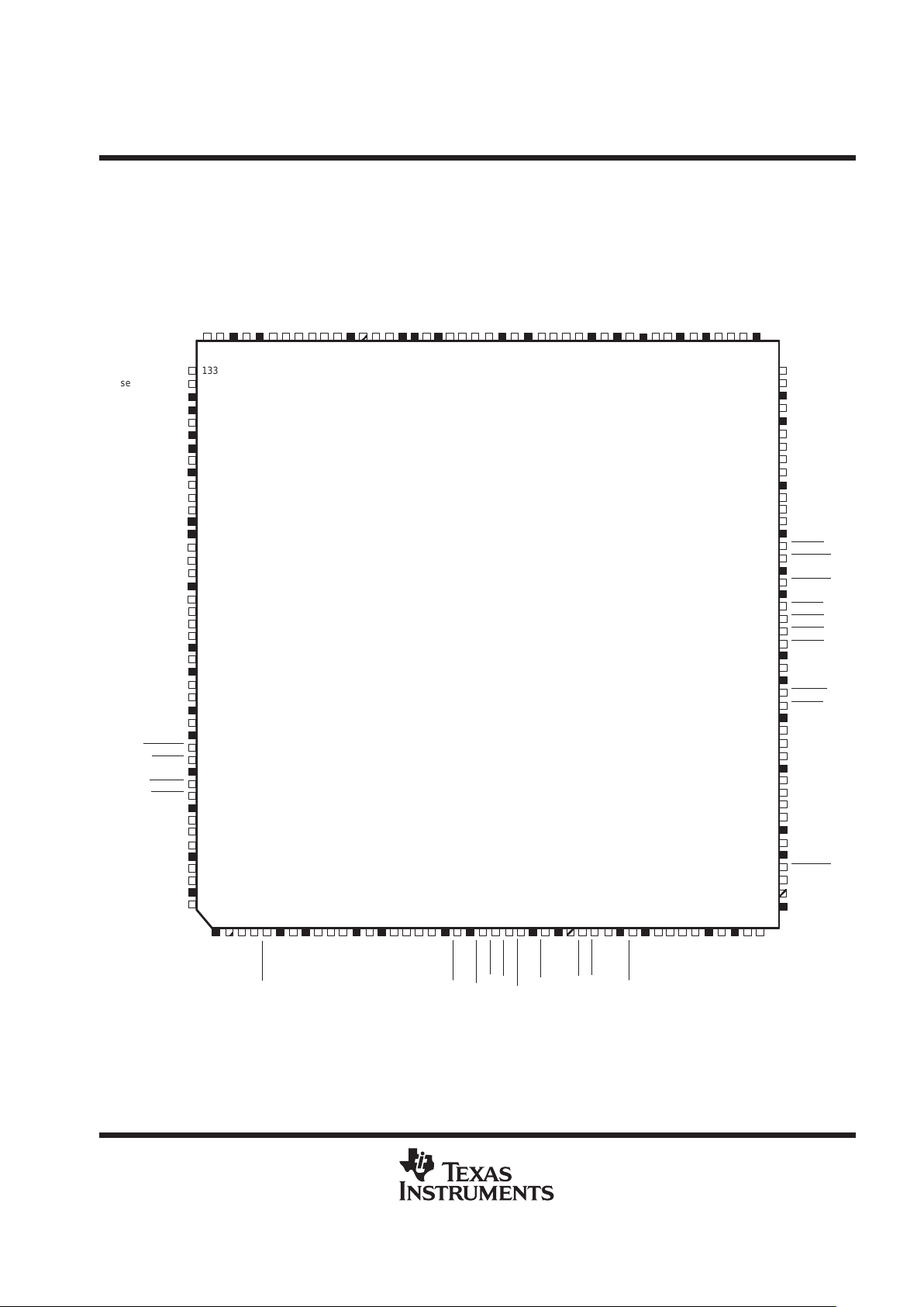
terminal assignment
PGF QUAD FLATPACK PACKAGE
TOP VIEW
seeprom_clk
50
75
aux_data15
phy_data0
pci_ad29
TSB12LV21B
133
seeprom_data 134
5V V
CC
135
3V V
CC
136
link_cyclein 137
3.3V V
CC
138
link_cycleout
139
test_out 140
GND 141
phy_ctl0 142
phy_ctl1
143
phy_lreq
144
3.3V V
CC
145
146
phy_data1
147
phy_data2 148
phy_data3 149
GND 150
phy_data4
151
phy_data5
152
phy_data6 153
phy_data7 154
GND 155
phy_clk50 156
3.3V V
CC
157
GND/test_enable 158
autoboot 159
GND 160
pci_clk
161
5V V
CC
162
pci_reset
163
pci_gnt
164
3.3V V
CC
165
pci_inta
166
pci_req
167
GND
168
pci_ad31 169
pci_ad30
170
171171
3.3V V
CC
172
pci_ad28
173
pci_ad27 174
GND
175
pci_ad26 176
3.3V V
CC
pci_ad7
aux_data6
aux_data787
3.3V V
CC
86
au_data885
5VV
CC
84
aux_data983
aux_data1082
aux_data1181
aux_data1280
GND79
aux_data1378
aux_data1477
76
aux_oe
74
aux_we0
73
GND72
aux_we1
71
3.3V V
CC
70
aux_cs
69
rom_cs
68
ram_cs67
aux_rst
66
GND65
aux_clk64
5V V
CC
63
aux_rdy
62
aux_int
61
5V V
CC
60
pci_ad059
pci_ad158
pci_ad257
3.3V V
CC
56
pci_ad355
pci_ad454
pci_ad5
pci_ad652
GND51
3.3V V
CC
49
pci_cbe0
48
pci_ad847
NC46
GND45
53
89
zv_data_valid
zv_hsync
GND
zv_ext_clk
3.3V VCCzv_vsync
zv_pix_clk
gpio_data0
gpio_data1
gpio_data2
gpio_data3
GND
132
131
130
129
128
127
126
125
124
123
122
121
120
119
118
117
116
115
114
113
112
111
110
aux_adr0NCaux_adr1
aux_adr2
3.3V VCCaux_adr3
GND
aux_adr4
aux_adr5
aux_adr6
aux_adr7
5V VCCaux_adr8
3.3V VCCaux_adr9
aux_adr10
109
108
107
106
105
104
103
102
101
100
9998979695949392919089
aux_adr11
aux_adr12
GND
aux_adr13
3.3V VCCaux_adr14
aux_adr15
aux_data0
aux_data1
GND
aux_data2
3.3V VCCaux_data3
aux_data4
aux_data5
GND
12345678910111213141516171819202122232425262728293031323334353637383940414243
44
3.3V V
CC
NC
pci_ad25
pci_ad24
pci_cbe3
GND
pci_idsel
3.3V V
CC
pci_ad23
pci_ad22
pci_ad21
5V V
CC
pci_ad20
GND
pci_ad19
pci_ad18
pci_ad17
pci_ad16
3.3V V
CC
GND
pci_frame
pci_irdy
pci_trdy
pci_devsel
pci_stop
3.3V V
CC
GND
NC
pci_cbe2
pci_perr
pci_serr
pci_par
3.3V V
CC
pci_cbe1
GND
pci_ad15
pci_ad14
pci_ad13
pci_ad12
5V V
CC
pci_ad11
3.3V V
CC
pci_ad10
pci_ad9
Figure 1. PCILynx-2 Terminal Assignment/Pinout

TSB12LV21B
(PCILynx-2) IEEE 1394 LINK LAYER CONTROLLER
SLLS306– JUL Y 1998
4
POST OFFICE BOX 655303 • DALLAS, TEXAS 75265
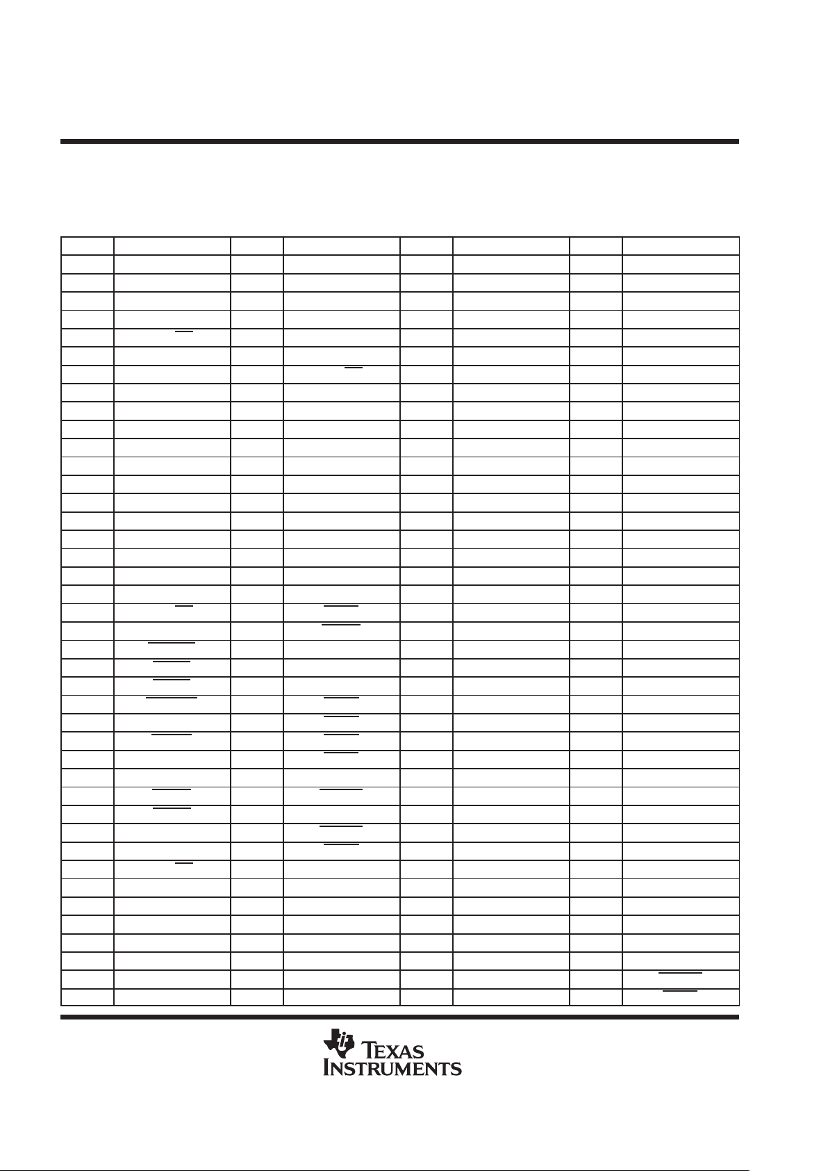
pin description table
This sections identifies and classifies the functionality of each pin on the PCILynx–2.
Table 1. Signals Sorted by Pin Number
PIN NO. SIGNAL NAME PIN NO. SIGNAL NAME PIN NO. SIGNAL NAME PIN NO. SIGNAL NAME
1 3.3V V
CC
42 3.3V V
CC
83 aux_data9 124 gpio_data1
2 NC 43 pci_ad10 84 5.0VV
CC
125 gpio_data0
3 pci_ad25 44 pci_ad9 85 aux_data8 126 zp_pix_clk
4 pci_ad24 45 GND 86 3.3V V
CC
127 zv_vsync
5 pci_cbe3 46 NC 87 aux_data7 128 3.3V V
CC
6 GND 47 pci_ad8 88 aux_data6 129 zv_ext_clk
7 pci_idsel 48 pci_cbe0 89 GND 130 GND
8 3.3V V
CC
49 3.3V V
CC
90 aux_data5 131 zv_hsync
9 pci_ad23 50 pci_ad7 91 aux_data4 132 zv_data_valid
10 pci_ad22 51 GND 92 aux_data3 133 seeprom_clk
11 pci_ad21 52 pci_ad6 93 3.3V V
CC
134 seeprom_data
12 5.0V V
CC
53 pci_ad5 94 aux_data2 135 5V V
CC
13 pci_ad20 54 pci_ad4 95 GND 136 3V V
CC
14 GND 55 pci_ad3 96 aux_data1 137 link_cyclein
15 pci_ad19 56 3.3V V
CC
97 aux_data0 138 3.3VV
CC
16 pci_ad18 57 pci_ad2 98 aux_adr15 139 link_cylceout
17 pci_ad17 58 pci_ad1 99 aux_adr14 140 test_out
18 pci_ad16 59 pci_ad0 100 3.3V V
CC
141 GND
19 3.3V V
CC
60 5.0V V
CC
101 aux_adr13 142 phy_ctl0
20 pci_cbe2 61 aux_int 102 GND 143 phy_ctl1
21 GND 62 aux_rdy 103 aux_adr12 144 phy_lreq
22 pci_frame 63 5.0V V
CC
104 aux_adr11 145 3.3V V
CC
23 pci_irdy 64 aux_clk 105 aux_adr10 146 phy_data0
24 pci_trdy 65 GND 106 aux_adr9 147 phy_data1
25 pci_devsel 66 aux_rst 107 3.3V V
CC
148 phy_data2
26 3.3V V
CC
67 ram_cs 108 aux_adr8 149 phy_data3
27 pci_stop 68 rom_cs 109 5.0V V
CC
150 GND
28 GND 69 aux_cs 110 aux_adr7 151 phy_data4
29 NC 70 3.3V V
CC
111 aux_adr6 152 phy_data5
30 pci_perr 71 aux_we1 112 aux_adr5 153 phy_data6
31 pci_serr 72 GND 113 aux_adr4 154 phy_data7
32 pci_par 73 aux_we0 114 GND 155 GND
33 3.3V V
CC
74 aux_oe 115 aux_adr3 156 phy_clk50
34 pci_cbe1 75 3.3V V
CC
116 3.3V V
CC
157 3.3V V
CC
35 GND 76 aux_data15 117 aux_adr2 158 test_out/GND
36 pci_ad15 77 aux_data14 118 aux_adr1 159 auto_boot
37 pci_ad14 78 aux_data13 119 aux_adr0 160 GND
38 pci_ad13 79 GND 120 NC 161 pci_clk
39 pci_ad12 80 aux_data12 121 GND 162 5.0V V
CC
40 5.0V V
CC
81 aux_data11 122 gpio_data3 163 pci_reset
41 pci_ad11 82 aux_data10 123 gpio_data2 164 pci_gnt

TSB12LV21B
(PCILynx-2) IEEE 1394 LINK LAYER CONTROLLER
SLLS306– JUL Y 1998
5
POST OFFICE BOX 655303 • DALLAS, TEXAS 75265
Table 1. Signals Sorted by Pin Number (Continued)
PIN NO. SIGNAL NAME PIN NO. SIGNAL NAME PIN NO. SIGNAL NAME PIN NO. SIGNAL NAME
165 3.3V V
CC
168 GND 171 pci_ad29 174 pci_ad27
166 pci_inta 169 pci_ad31 172 3.3V V
CC
175 GND
167 pci_req 170 pci_ad30 173 pci_ad28 176 pci_ad26
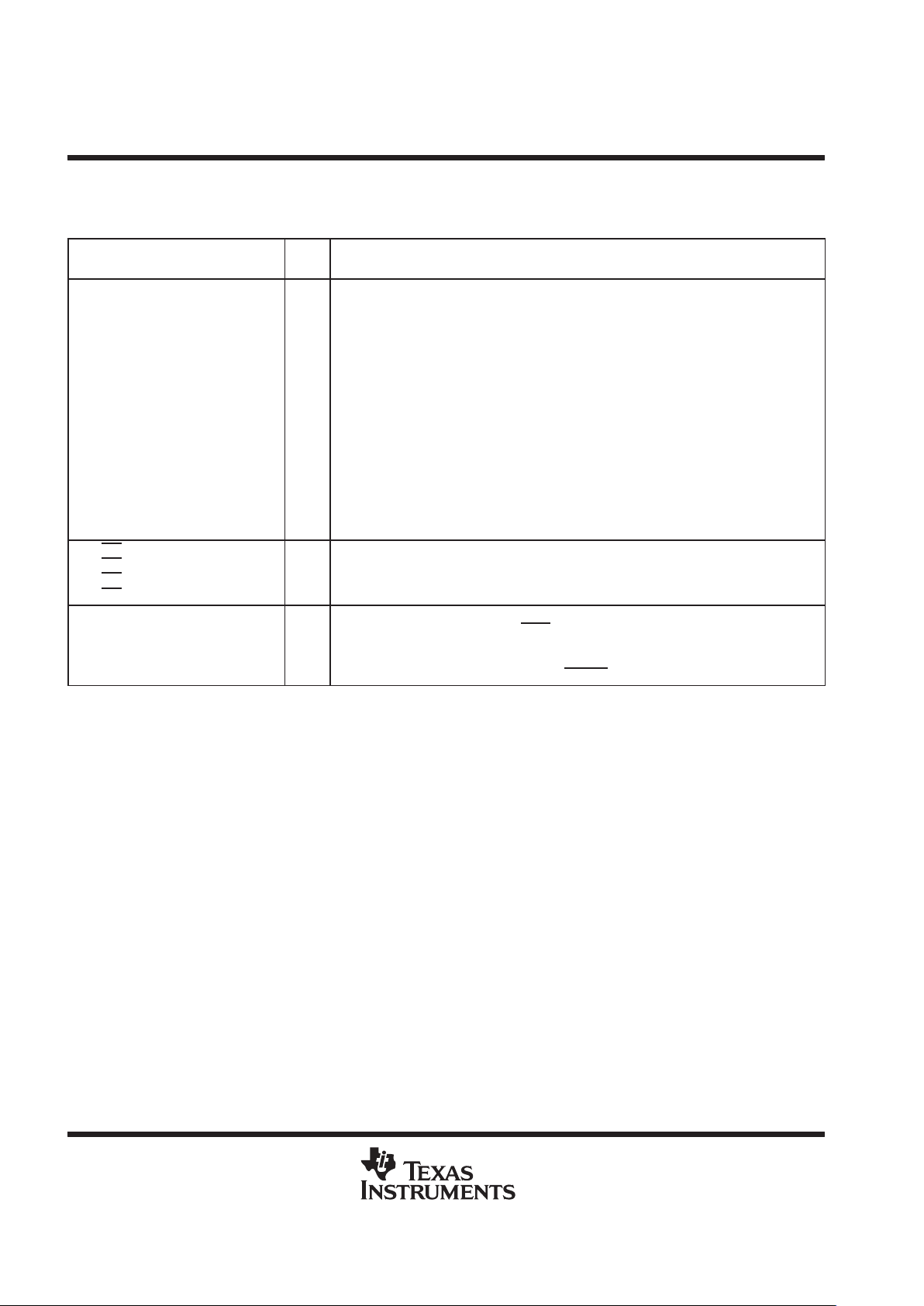
Terminal Functions
power supply terminals
TERMINAL
I/O
NAME NO.
I/O
TYPE
FUNCTION
GND
6, 14, 21, 28, 35, 45,
51, 65, 72, 79, 89,
95, 102, 114, 121,
130, 141, 150, 155,
160, 168, 175
I Device ground terminals
3.3V VCC
1, 8, 19, 26, 33, 42,
49, 56, 70, 75, 86,
93, 100, 107, 116,
128, 136, 138, 145,
157, 165, 172
I 3.3-V power supply terminal for core logic
5.0V VCC
12, 40, 60, 63, 84,
109, 162
I 5-V power rail for 5-V tolerant Input buffers
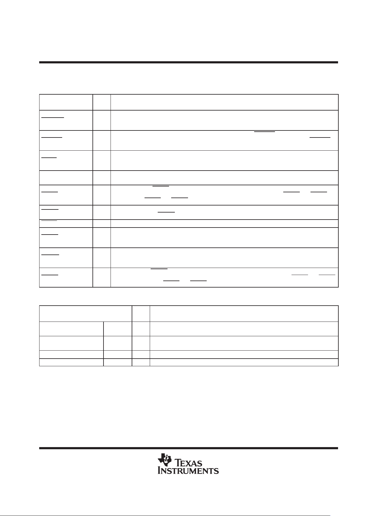
PCI system terminals
TERMINAL
I/O
NAME NO.
I/O
TYPE
FUNCTION
pci_clk 161 I
System PCI bus clock. This signal ranges from 0MHz–-33MHz MHz and provides timing for all transactions
on the PCI bus. All PCI signals are sampled at the rising edge of PCLK.
pci_reset 163 I
pci_reset. When the PCI bus reset is asserted the pci_reset signal causes the PCILynx-2 to 3-state all
output buffers and reset all internal registers. When pci_reset
is asserted, the device is completely
nonfunctional. After pci_reset
is deasserted, the PCILynx-2 is in its default state.
pci_inta 166 OD PCI system interrupt A. This is an open drain signal.

TSB12LV21B
(PCILynx-2) IEEE 1394 LINK LAYER CONTROLLER
SLLS306– JUL Y 1998
6
POST OFFICE BOX 655303 • DALLAS, TEXAS 75265
Terminal Functions (Continued)
PCI address and data terminals
TERMINAL
I/O
NAME NO.
I/O
TYPE
FUNCTION
pci_ad31 – pci_ad29
pci_ad28
pci_ad27
pci_ad26
pci_ad25
pci_ad24
pci_ad23 – pci_ad21
pci_ad20
pci_ad19 – pci_ad16
pci_ad15 – pci_ad12
pci_ad1 1
pci_ad10
pci_ad9
pci_ad8
pci_ad7
pci_ad6 – pci_ad3
pci_ad2 – pci_ad0
169 – 171
173
174
176
3
4
9 – 11
13
15 – 18
36 – 39
41
43
44
47
50
52 – 55
57 – 59
I/O
Multiplexed PCI address and data signals. During the address phase of a primary bus PCI
cycle, pci_ad31:0 contain a 32-bit address or other destination information. During the data
phase pci_ad31:0 contain data
pci_cbe3
pci_cbe2
pci_cbe1
pci_cbe0
5
20
34
48
I/O PCI Command/Byte enables
pci_par 32 I/O
PCI bus parity. In all PCI bus read and write cycles the PCILynx–2 calculates even paritacross the pci_ad31:0 and pci_cbe3:0
signals. As an initiator during PCI cycles, the
PCILynx-2 outputs this parity indicator with a one pci_clk delay. As a target during PCI
cycles, the calculated parity is compared to the initiator’s parity indicator. A miscompare
can result in the assertion of a parity error (pci_perr
).

TSB12LV21B
(PCILynx-2) IEEE 1394 LINK LAYER CONTROLLER
SLLS306– JUL Y 1998
7
POST OFFICE BOX 655303 • DALLAS, TEXAS 75265
Terminal Functions (Continued)
PCI interface control
TERMINAL
I/O
NAME NO.
I/O
TYPE
FUNCTION
pci_devsel 24 I/O
PCI device select. The PCILynx-2 asserts this signal to claim a PCI cycle as the target device. As a PCI
initiator on the bus, the PCILynx-2 monitors this signal until a target responds. If no target responds before
time-out occurs, then the PCILynx-2 will terminate the cycle with an initiator abort.
pci_frame 22 I/O
PCI cycle frame. This signal is driven by the initiator of a bus cycle. pci_frame is asserted to indicate that a
bus transaction is beginning, and data transfers continue while this signal is asserted. When pci_frame
is
deasserted the PCI bus transaction is in the final data phase.
pci_gnt 164 I
PCI bus grant. This signal is driven by the PCI bus arbiter to grant the PCILynx-2 access to the PCI bus
after the current data transaction has completed. This signal may or may not follow a PCI bus request
depending upon the PCI bus parking algorithm.
pci_idsel 7 I
Initialization device select. pci_idsel selects the PCILynx-2 during configuration space accesses. pci_idsel
can be connected to one of the upper 24 PCI address lines on the PCI bus.
pci_irdy 23 I/O
PCI initiator ready. pci_irdy indicates the PCI bus initiator’s ability to complete the current data phase of the
transaction. A data phase is completed upon a rising edge of pci_clk where both pci_irdy
and pci_trdy are
asserted. Until pci_irdy
and pci_trdy are both sampled asserted, wait states are inserted.
pci_perr 30 I/O
PCI parity error indicator. This signal is driven by a PCI device to indicate that calculated parity does not
match pci_par, when pci_perr
is enabled through bit 6 of the command register.
pci_req 167 O PCI bus request. Asserted by the PCIL ynx-2 to request access to the PCI bus as an initiator.
pci_serr 31 OD
PCI system error. Output that is pulsed from the PCILynx-2 when enabled through the command register,
indicating a system error has occurred. The PCILynx-2 needs not be the target of the PCI cycle in order to
assert this signal.
pci_stop 27 I/O
PCI cycle stop signal. This signal is driven by a PCI target to request the initiator to stop the current PCI
bus transaction. This signal is used for target disconnects and is commonly asserted by target devices
which do not support burst data transfers.
pci_trdy 24 I/O
PCI target ready. pci_trdy indicates the primary bus target’s ability to complete the current data phase of
the transaction. A data phase is completed upon a rising edge of pci_clk where both pci_irdy
and pci_trdy
are asserted. Until both pci_irdy and pci_trdy are asserted, wait states are inserted.
IEEE 1394 PHY/LINK interface terminals
TERMINAL
I/O
NAME NO.
I/O
TYPE
FUNCTION
phy_ctl1
phy_ctl0
143
142
I/O PHY -link bidirectional control lines
phy_data7 – phy_data4
phy_data3 – phy_data0
154 – 151
149 – 146
I/O PHY -link bidirectional data lines
phy_clk50 156 I 50MHz-System clock from PHY chip
phy_lreq 144 O PHY -link request signal generated by the PCILynx-2 controller
 Loading...