TRF7003
MOSFET POWER AMPLIFIER
SLWS058C – APRIL 1997 – REVISED JULY 1998
1
POST OFFICE BOX 655303 • DALLAS, TEXAS 75265
D
Wide Operating Frequency Range up to
1000 MHz
D
High Output Power:
– Typical Value of 32 dBm at 4.8 V and 900
MHz
– Typical Value of 29 dBm at 3.6 V and
900 MHz
D
High Gain:
– Typical Value of 9 dB at 4.8 V and
900 MHz at 32-dBm Output Power
D
High Power-Added Efficiency (PAE):
– Typical Value of 50% at 32-dBm Output
Power
D
Low Cost
D
Extremely Rugged:
– Sustains 20:1 Load Mismatch
D
Suitable for Various Wireless Applications
D
Low Leakage Current <1 mA
D
SOT-89 Plastic Power Package
D
1000 V Human Body Model ESD Protection
on Gate and Drain
description
The TRF7003 power amplifier is a silicon, metal-oxide semiconductor, field-effect transistor (MOSFET)
manufactured using the Texas Instruments RFMOS process. It is housed in a SOT-89 (PK) plastic power
package. The TRF7003, suitable for a variety of wireless applications, has been characterized for global
systems for mobile communications (GSM) power amplifier applications. The TRF7003, a rugged, low-cost
device, operates from a single-polarity positive power supply and has low leakage current. Typical power output
at 900 MHz is 32 dBm, with an associated power gain of 9 dB and 50-percent power-added efficiency (PAE).
Copyright 1998, Texas Instruments Incorporated
PRODUCTION DATA information is current as of publication date.
Products conform to specifications per the terms of Texas Instruments
standard warranty. Production processing does not necessarily include
testing of all parameters.
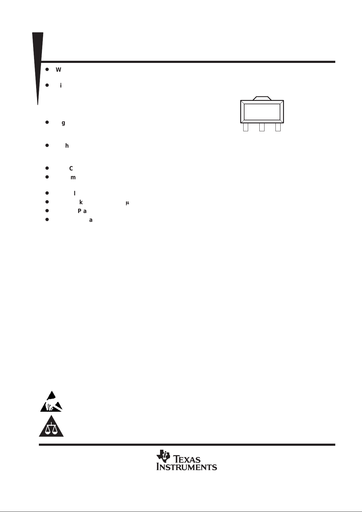
GSD
PK PACKAGE
(TOP VIEW)
These devices have limited built-in ESD protection. The leads should be shorted together or the device placed in conductive foam
during storage or handling to prevent electrostatic damage to the MOS gates.
Please be aware that an important notice concerning availability, standard warranty, and use in critical applications of
Texas Instruments semiconductor products and disclaimers thereto appears at the end of this data sheet.
RFMOS is a trademark of Texas Instruments Incorporated.

TRF7003
MOSFET POWER AMPLIFIER
SLWS058C – APRIL 1997 – REVISED JULY 1998
2
POST OFFICE BOX 655303 • DALLAS, TEXAS 75265
absolute maximum ratings over operating free-air temperature range (unless otherwise noted)
†
Drain-source voltage, V
DS
15 V. . . . . . . . . . . . . . . . . . . . . . . . . . . . . . . . . . . . . . . . . . . . . . . . . . . . . . . . . . . . . . . . . .
Gate-source voltage, V
GS
7 V. . . . . . . . . . . . . . . . . . . . . . . . . . . . . . . . . . . . . . . . . . . . . . . . . . . . . . . . . . . . . . . . . . . .
Continuous drain current, I
D
2 A. . . . . . . . . . . . . . . . . . . . . . . . . . . . . . . . . . . . . . . . . . . . . . . . . . . . . . . . . . . . . . . . . .
Junction temperature, T
J max
150°C. . . . . . . . . . . . . . . . . . . . . . . . . . . . . . . . . . . . . . . . . . . . . . . . . . . . . . . . . . . . . .
Thermal resistance, junction to case, R
θJC
(See Note 1) 10°C/W. . . . . . . . . . . . . . . . . . . . . . . . . . . . . . . . . . . . .
Total device power dissipation at T
C
= 25°C 12.5 W. . . . . . . . . . . . . . . . . . . . . . . . . . . . . . . . . . . . . . . . . . . . . . . . .
Derate above 25°C 100 mW/°C. . . . . . . . . . . . . . . . . . . . . . . . . . . . . . . . . . . . . . . . . . . . . . . . . . . . . . . . . . . . . . . .
Operating free-air temperature range,T
A
–40°C to 85°C. . . . . . . . . . . . . . . . . . . . . . . . . . . . . . . . . . . . . . . . . . . .
Storage temperature range, T
stg
–65°C to 100°C. . . . . . . . . . . . . . . . . . . . . . . . . . . . . . . . . . . . . . . . . . . . . . . . . . .
ESD protection, gate and drain, human body model 1000 V. . . . . . . . . . . . . . . . . . . . . . . . . . . . . . . . . . . . . . . . . .
†
Stresses beyond those listed under “absolute maximum ratings” may cause permanent damage to the device. These are stress ratings only, and
functional operation of the device at these or any other conditions beyond those indicated under ”recommended operating conditions” is not
implied. Exposure to absolute-maximum-rated conditions for extended periods may affect device reliability.
NOTE 1: With infinite heatsink and no air flow
electrical characteristics over operating free-air temperature range (unless otherwise noted)
dc characteristics
LIMITS
PARAMETER
TEST CONDITIONS
‡
MIN TYP MAX
UNITS
I
D
Saturated drain current VDS = 4.8 V, VGS = 1.7 V 0.7 A
g
m
Transconductance VDS = 4.8 V, VGS = 1.7 V 1000 mS
V
(TO)
Threshold voltage VDS = 100mV , IDS = 1.5 mA 1.0 V
V(BR)sdSource-drain breakdown voltage
Ids = 40 µA,
Source is grounded
VGS = 0 V
16 V
Leakage current VDS = 4.8 V VGS = 0 V <1 µA
‡
TA = 25°C
RF characteristics, VDS = 4.8 V, VGS = 1.7 V
LIMITS
PARAMETER
TEST CONDITIONS
§
MIN TYP MAX
UNITS
Output power Frequency = 900 MHz, PI = 23 dBm 31 32 dBm
Power gain Frequency = 900 MHz, PI = 23 dBm 9 dB
η
add
Power added efficiency Frequency = 900 MHz, PI = 23 dBm 45% 50%
Ruggedness test
Frequency = 900 MHz,
Load VSWR = 20:1,
PI = 23 dBm,
All phase angles
¶
§
TA = 25°C, fixed matching circuit
¶
No degradation in output power after test.

TRF7003
MOSFET POWER AMPLIFIER
SLWS058C – APRIL 1997 – REVISED JULY 1998
3
POST OFFICE BOX 655303 • DALLAS, TEXAS 75265
TYPICAL CHARACTERISTICS
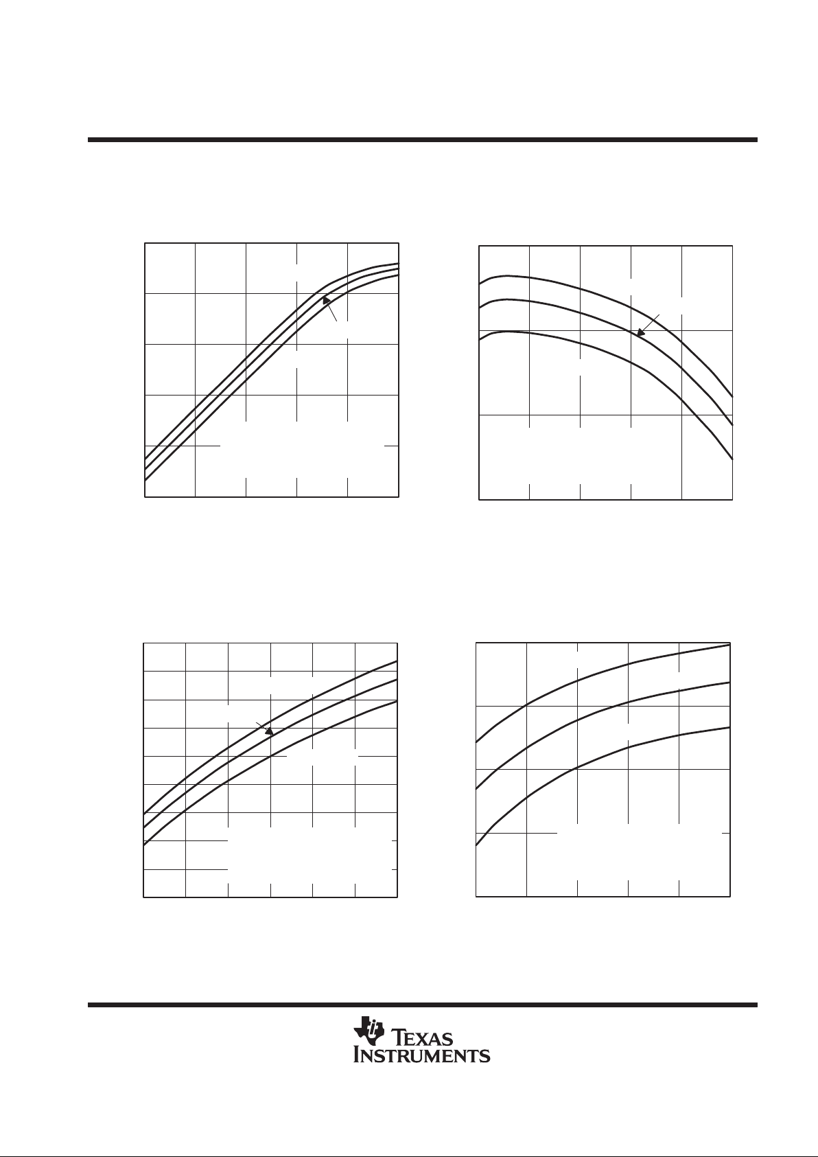
Figure 1
TA = –40°C
TA = 25°C
TA = 85°C
4.8 V GSM Application Circuit
VDS = 4.8 V
VGS = 1.7 V
Frequency = 900 MHz
20
15
10
0 5 10 15
– Output Power – dBm
25
30
OUTPUT POWER
vs
INPUT POWER
35
20 25
P
O
PI – Input Power – dBm
Figure 2
4.8 V GSM Application Circuit
VDS = 4.8 V
VGS = 1.7 V
PI = 23 dBm
TA = –40°C
TA = 25°C
TA = 85°C
30
28
850 870 890 910
32
f – Frequency – MHz
OUTPUT POWER
vs
FREQUENCY
34
930 950
– Output Power – dBm
P
O
Figure 3
TA = –40°C
TA = 25°C
TA = 85°C
4.8 V GSM Application Circuit
VGS = 1.7 V
PI = 23 dBm
Frequency = 900 MHz
31
29
27
26
3 3.5 4 4.5
32
34
OUTPUT POWER
vs
DRAIN VOLTAGE
35
5 5.5 6
– Output Power – dBm
P
O
33
30
28
VDD – Drain Voltage – V
TA = –40°C
TA = 25°C
TA = 85°C
4.8 V GSM Application Circuit
VDD = 4.8 V
PI = 23 dBm
Frequency = 900 MHz
31
30
29
1 1.2 1.4 1.6
32
OUTPUT POWER
vs
GATE VOLTAGE
(MAX POWER ADDED EFFICIENCY TUNING)
33
1.8 2
– Output Power – dBm
P
O
VGS – Gate Voltage – V
Figure 4
 Loading...