

Page 1

User’s G uide
April 2002 Mixed-Signal RF Products
SWRU006A
Page 2

EVM IMPORTANT NOTICE
Texas Instruments (TI) provides the enclosed product(s) under the following conditions:
This evaluation kit being sold by TI is intended for use for ENGINEERING DEVELOPMENT OR EVALUATION
PURPOSES ONLY and is not considered by TI to be fit for commercial use. As such, the goods being provided
may not be complete in terms of required design-, marketing-, and/or manufacturing-related protective
considerations, including product safety measures typically found in the end product incorporating the goods.
As a prototype, this product does not fall within the scope of the European Union directive on electromagnetic
compatibility and therefore may not meet the technical requirements of the directive.
Should this evaluation kit not meet the specifications indicated in the EVM User’s Guide, the kit may be returned
within 30 days from the date of delivery for a full refund. THE FOREGOING WARRANTY IS THE EXCLUSIVE
WARRANTY MADE BY SELLER TO BUYER AND IS IN LIEU OF ALL OTHER WARRANTIES, EXPRESSED,
IMPLIED, OR S TA TUTOR Y, INCLUDING ANY WARRANTY OF MERCHANTABILITY OR FITNESS FOR ANY
PARTICULAR PURPOSE.
The user assumes all responsibility and liability for proper and safe handling of the goods. Further, the user
indemnifies TI from all claims arising from the handling or use of the goods. Please be aware that the products
received may not be regulatory compliant or agency certified (FCC, UL, CE, etc.). Due to the open construction
of the product, it is the user’s responsibility to take any and all appropriate precautions with regard to electrostatic
discharge.
EXCEPT TO THE EXTENT OF THE INDEMNITY SET FORTH ABOVE, NEITHER PARTY SHALL BE LIABLE
TO THE OTHER FOR ANY INDIRECT, SPECIAL, INCIDENTAL, OR CONSEQUENTIAL DAMAGES.
TI currently deals with a variety of customers for products, and therefore our arrangement with the user is not
exclusive.
TI assumes no liability for applications assistance, customer product design, software performance, or
infringement of patents or services described herein.
Please read the EVM User’s Guide and, specifically, the EVM Warnings and Restrictions notice in the EVM
User’s Guide prior to handling the product. This notice contains important safety information about temperatures
and voltages. For further safety concerns, please contact the TI application engineer.
Persons handling the product must have electronics training and observe good laboratory practice standards.
No license is granted under any patent right or other intellectual property right of TI covering or relating to any
machine, process, or combination in which such TI products or services might be or are used.
Mailing Address:
Texas Instruments
Post Office Box 655303
Dallas, Texas 75265
Copyright 2002, Texas Instruments Incorporated
Page 3

EVM WARNINGS AND RESTRICTIONS
It is important to operate this EVM within the specified input and output ranges described in
the EVM User’s Guide.
Exceeding the specified input range may cause unexpected operation and/or irreversible
damage to the EVM. If there are questions concerning the input range, please contact a TI
field representative prior to connecting the input power.
Applying loads outside of the specified output range may result in unintended operation and/or
possible permanent damage to the EVM. Please consult the EVM User’s Guide prior to
connecting any load to the EVM output. If there is uncertainty as to the load specification,
please contact a TI field representative.
During normal operation, some circuit components may have case temperatures greater than
60°C. The EVM is designed to operate properly with certain components above 60°C as long
as the input and output ranges are maintained. These components include but are not limited
to linear regulators, switching transistors, pass transistors, and current sense resistors. These
types of devices can be identified using the EVM schematic located in the EVM User’s Guide.
When placing measurement probes near these devices during operation, please be aware
that these devices may be very warm to the touch.
Mailing Address:
Texas Instruments
Post Office Box 655303
Dallas, Texas 75265
Copyright 2002, Texas Instruments Incorporated
Page 4

Page 5

About This Manual
How to Use This Manual
Preface
This document presents the contents of the TRF6901 868 MHz to 870 MHz
RF tool kit. Both hardware and software are described in detail. The first half
of the document addresses the TRF6901 RF EVM in a stand-alone evaluation
environment. The second half of the document addresses the TRF6901 serial
port module that is used to support the TRF6901 RF EVM evaluation in a
system environment configuration.
It is important when reading this document to remember that the TRF6901
serial port module is a support module provided along with the TFR6901 RF
EVM contained in the TRF6901 RF tool kit. The TRF6901 serial port module
is NOT to be considered a stand-alone tool.
Using this document, the user will understand the features of the TRF6901 RF
EVM as well as the features of the TRF6901 serial port module as it relates
to the TRF6901 RF EVM. Also, the user will become familiar with the features
and functionality of both the TRF6901 EVM and the TRF6901 serial port tools
software packages.
With the TRF6901 EVM software package, the user will understand how to
evaluate the functionality of the TRF6901 on the TRF6901 RF EVM via a PC
parallel port. With the serial port software package, the user will understand
how to use the programming tool to evaluate the TRF6901 via the PC serial
port connection to the TRF6901 serial port module.
Finally, along with being exposed to the basic structure and protocol of an RF
link example, the user will be able to use the system mode tool contained within
the TRF6901 serial port tools software to establish a basic RF link using two
TRF6901 RF tool kits.
Evaluation Board Disclaimer
Please note that the enclosed evaluation boards are experimental printed
circuit boards and are therefore only intended for device evaluation.
We would like to draw your attention to the fact that these boards have been
processed through one or more of Texas Instruments’ external subcontractors
which have not been production qualified.
v
Page 6

Information About Cautions and Warnings
The fee associated with the evaluation modules (EVM) is a partial
nonrecurring engineering fee (NRE) to partially defray the engineering costs
associated with the EVM development and applications support for the RF
integrated semiconductor product. The EVM is a tool for evaluating the RF
semiconductors supplied by Texas Instruments. The EVM is supplied to
prospective component customers to provide services and software allowing
the prospect customers to evaluate the RF semiconductors in products they
would build.
The EVM may be operated only for product evaluation purposes and then only
in nonresidential areas. TI’s understanding is that the customers’ products
using the RF parts listed shall be designed to comply with all applicable FCC
and appropriate regulatory agency requirements and will, upon testing,
comply with these requirements. Operation of this device is subject to the
conditions that it does not cause harmful interference and that it must accept
any interference.
How to Use This Manual
This document contains the following chapters:
- Chapter 1—TRF6901 RF Tool Kit Overview
- Chapter 2—TRF6901 RF EVM PCB Hardware
- Chapter 3—TRF6901 EVM Control Software
- Chapter 4—TRF6901 Serial Port Tool Overview
- Chapter 5—TRF6901 Serial Port Module PCB Hardware
- Chapter 6—TRF6901 RF Tool Kit System Mode
- Chapter 7—TRF6901 Serial Port Tools Software
Information About Cautions and Warnings
This book may contain cautions and warnings.
This is an example of a caution statement.
A caution statement describes a situation that could potentially
damage your software or equipment.
This is an example of a warning statement.
A warning statement describes a situation that could potentially
cause harm to you
.
The information in a caution or a warning is provided for your protection.
Please read each caution and warning carefully.
vi
Page 7

Contents
1 TRF6901 RF Tool Kit Overview 1-1. . . . . . . . . . . . . . . . . . . . . . . . . . . . . . . . . . . . . . . . . . . . . . . . . . .
1.1 Description 1-2. . . . . . . . . . . . . . . . . . . . . . . . . . . . . . . . . . . . . . . . . . . . . . . . . . . . . . . . . . . . . . . .
1.2 Contents 1-2. . . . . . . . . . . . . . . . . . . . . . . . . . . . . . . . . . . . . . . . . . . . . . . . . . . . . . . . . . . . . . . . . .
1.3 TRF6901 EVM/Parallel Port Configuration 1-2. . . . . . . . . . . . . . . . . . . . . . . . . . . . . . . . . . . . .
1.4 TRF6901 EVM/Serial Port Module Configuration 1-2. . . . . . . . . . . . . . . . . . . . . . . . . . . . . . . .
2 TRF6901 RF EVM PCB Hardware 2-1. . . . . . . . . . . . . . . . . . . . . . . . . . . . . . . . . . . . . . . . . . . . . . . . .
2.1 Hardware Overview 2-2. . . . . . . . . . . . . . . . . . . . . . . . . . . . . . . . . . . . . . . . . . . . . . . . . . . . . . . . .
2.2 TRF6901 RF Block Diagram 2-2. . . . . . . . . . . . . . . . . . . . . . . . . . . . . . . . . . . . . . . . . . . . . . . . .
2.3 TRF6901 RF EVM Schematics 2-3. . . . . . . . . . . . . . . . . . . . . . . . . . . . . . . . . . . . . . . . . . . . . . .
2.4 Top- and Bottom-Side Silkscreen and Drawing 2-5. . . . . . . . . . . . . . . . . . . . . . . . . . . . . . . . .
2.5 Parts List 2-6. . . . . . . . . . . . . . . . . . . . . . . . . . . . . . . . . . . . . . . . . . . . . . . . . . . . . . . . . . . . . . . . . .
2.6 TRF6901 RF EVM Regulated Supply Configuration 2-11. . . . . . . . . . . . . . . . . . . . . . . . . . . .
2.7 TRF6901 Parallel Port Module Interface 2-12. . . . . . . . . . . . . . . . . . . . . . . . . . . . . . . . . . . . . .
2.8 TRF6901 RF EVM Jumpers 2-13. . . . . . . . . . . . . . . . . . . . . . . . . . . . . . . . . . . . . . . . . . . . . . . . .
2.8.1 Jumper Connections 2-13. . . . . . . . . . . . . . . . . . . . . . . . . . . . . . . . . . . . . . . . . . . . . . . .
2.8.2 Default Jumper Connections 2-15. . . . . . . . . . . . . . . . . . . . . . . . . . . . . . . . . . . . . . . . .
2.8.3 Jumper Description 2-15. . . . . . . . . . . . . . . . . . . . . . . . . . . . . . . . . . . . . . . . . . . . . . . . .
2.9 Connectors 2-16. . . . . . . . . . . . . . . . . . . . . . . . . . . . . . . . . . . . . . . . . . . . . . . . . . . . . . . . . . . . . . .
2.10 Test Points (TP) 2-17. . . . . . . . . . . . . . . . . . . . . . . . . . . . . . . . . . . . . . . . . . . . . . . . . . . . . . . . . . .
2.11 Adjustments 2-18. . . . . . . . . . . . . . . . . . . . . . . . . . . . . . . . . . . . . . . . . . . . . . . . . . . . . . . . . . . . . .
2.12 LED Indicators 2-19. . . . . . . . . . . . . . . . . . . . . . . . . . . . . . . . . . . . . . . . . . . . . . . . . . . . . . . . . . . .
3 TRF6901 RF EVM Control Software 3-1. . . . . . . . . . . . . . . . . . . . . . . . . . . . . . . . . . . . . . . . . . . . . . .
3.1 TRF6901 RF EVM Control Software Overview 3-2. . . . . . . . . . . . . . . . . . . . . . . . . . . . . . . . . .
3.2 TRF6901 RF EVM Control Software Installation 3-2. . . . . . . . . . . . . . . . . . . . . . . . . . . . . . . .
3.3 TRF6901 RF EVM Setup With Control Software 3-2. . . . . . . . . . . . . . . . . . . . . . . . . . . . . . . .
3.4 How to Use the TRF6901 Control Software 3-3. . . . . . . . . . . . . . . . . . . . . . . . . . . . . . . . . . . .
3.5 Main Program Screen 3-3. . . . . . . . . . . . . . . . . . . . . . . . . . . . . . . . . . . . . . . . . . . . . . . . . . . . . . .
3.5.1 Synthesizer 3-4. . . . . . . . . . . . . . . . . . . . . . . . . . . . . . . . . . . . . . . . . . . . . . . . . . . . . . . . .
3.5.2 Mode Options 3-6. . . . . . . . . . . . . . . . . . . . . . . . . . . . . . . . . . . . . . . . . . . . . . . . . . . . . . .
3.5.3 Operating Modes 3-8. . . . . . . . . . . . . . . . . . . . . . . . . . . . . . . . . . . . . . . . . . . . . . . . . . . .
3.5.4 Help Box 3-9. . . . . . . . . . . . . . . . . . . . . . . . . . . . . . . . . . . . . . . . . . . . . . . . . . . . . . . . . . .
3.5.5 Words 3-9. . . . . . . . . . . . . . . . . . . . . . . . . . . . . . . . . . . . . . . . . . . . . . . . . . . . . . . . . . . . .
3.5.6 Operation Mode 3-9. . . . . . . . . . . . . . . . . . . . . . . . . . . . . . . . . . . . . . . . . . . . . . . . . . . . .
3.5.7 The Menu Bar 3-9. . . . . . . . . . . . . . . . . . . . . . . . . . . . . . . . . . . . . . . . . . . . . . . . . . . . . . .
3.6 IC Layout Screen 3-10. . . . . . . . . . . . . . . . . . . . . . . . . . . . . . . . . . . . . . . . . . . . . . . . . . . . . . . . . .
3.6.1 Main IC Layout Form 3-10. . . . . . . . . . . . . . . . . . . . . . . . . . . . . . . . . . . . . . . . . . . . . . . .
3.6.2 Options 3-12. . . . . . . . . . . . . . . . . . . . . . . . . . . . . . . . . . . . . . . . . . . . . . . . . . . . . . . . . . .
vii
Page 8

Contents
3.6.3 FSK/OOK Test 3-13. . . . . . . . . . . . . . . . . . . . . . . . . . . . . . . . . . . . . . . . . . . . . . . . . . . . .
3.7 Testing the Transmitter 3-13. . . . . . . . . . . . . . . . . . . . . . . . . . . . . . . . . . . . . . . . . . . . . . . . . . . . .
3.7.1 Step 1: Test Setup 3-13. . . . . . . . . . . . . . . . . . . . . . . . . . . . . . . . . . . . . . . . . . . . . . . . .
3.7.2 Step 2: Software Programming 3-14. . . . . . . . . . . . . . . . . . . . . . . . . . . . . . . . . . . . . .
3.7.3 Step 3: Spectrum Analyzer Setup 3-16. . . . . . . . . . . . . . . . . . . . . . . . . . . . . . . . . . . .
3.7.4 Step 4: FSK Modulation Output Test 3-17. . . . . . . . . . . . . . . . . . . . . . . . . . . . . . . . . .
3.7.5 FSK Test Using an External Source 3-18. . . . . . . . . . . . . . . . . . . . . . . . . . . . . . . . . . .
3.8 Testing of the Receiver 3-20. . . . . . . . . . . . . . . . . . . . . . . . . . . . . . . . . . . . . . . . . . . . . . . . . . . . .
3.8.1 Test Equipment Setup 3-20. . . . . . . . . . . . . . . . . . . . . . . . . . . . . . . . . . . . . . . . . . . . . . .
3.8.2 Software Programming for Receiver Testing 3-21. . . . . . . . . . . . . . . . . . . . . . . . . . .
3.8.3 LEARN and HOLD Modes 3-22. . . . . . . . . . . . . . . . . . . . . . . . . . . . . . . . . . . . . . . . . . .
3.8.4 Measured Receive Data 3-23. . . . . . . . . . . . . . . . . . . . . . . . . . . . . . . . . . . . . . . . . . . . .
4 TRF6901 Serial Port Tool Overview 4-1. . . . . . . . . . . . . . . . . . . . . . . . . . . . . . . . . . . . . . . . . . . . . . .
4.1 Purpose 4-2. . . . . . . . . . . . . . . . . . . . . . . . . . . . . . . . . . . . . . . . . . . . . . . . . . . . . . . . . . . . . . . . . . .
4.2 TRF6901 Serial Port Module Description 4-2. . . . . . . . . . . . . . . . . . . . . . . . . . . . . . . . . . . . . .
5 TRF6901 Serial Port Module PCB Hardware 5-1. . . . . . . . . . . . . . . . . . . . . . . . . . . . . . . . . . . . . . .
5.1 Hardware Overview 5-2. . . . . . . . . . . . . . . . . . . . . . . . . . . . . . . . . . . . . . . . . . . . . . . . . . . . . . . . .
5.2 PC Serial Port Interface 5-5. . . . . . . . . . . . . . . . . . . . . . . . . . . . . . . . . . . . . . . . . . . . . . . . . . . . .
5.3 MSP430 Features 5-5. . . . . . . . . . . . . . . . . . . . . . . . . . . . . . . . . . . . . . . . . . . . . . . . . . . . . . . . . .
5.4 TRF6901 SV1 Interface 5-6. . . . . . . . . . . . . . . . . . . . . . . . . . . . . . . . . . . . . . . . . . . . . . . . . . . . .
5.5 Control Signal Interface J12 5-7. . . . . . . . . . . . . . . . . . . . . . . . . . . . . . . . . . . . . . . . . . . . . . . . . .
5.6 JTAG Interface J13 5-7. . . . . . . . . . . . . . . . . . . . . . . . . . . . . . . . . . . . . . . . . . . . . . . . . . . . . . . . .
5.7 Miscellaneous MSP430 Port Terminals 5-7. . . . . . . . . . . . . . . . . . . . . . . . . . . . . . . . . . . . . . . .
5.8 LED Status Indicators 5-7. . . . . . . . . . . . . . . . . . . . . . . . . . . . . . . . . . . . . . . . . . . . . . . . . . . . . . .
6 TRF6901 RF Tool Kit System Mode 6-1. . . . . . . . . . . . . . . . . . . . . . . . . . . . . . . . . . . . . . . . . . . . . . .
6.1 TRF6901 RF Tool Kit System Mode Overview 6-2. . . . . . . . . . . . . . . . . . . . . . . . . . . . . . . . . .
6.1.1 Protocol Used by the System Mode RF Link 6-2. . . . . . . . . . . . . . . . . . . . . . . . . . . .
6.1.2 Specification Followed for the System Mode RF Link Example 6-2. . . . . . . . . . . .
6.2 System Mode Description 6-3. . . . . . . . . . . . . . . . . . . . . . . . . . . . . . . . . . . . . . . . . . . . . . . . . . . .
6.2.1 System Mode Tool Kit Configuration 6-3. . . . . . . . . . . . . . . . . . . . . . . . . . . . . . . . . . .
6.2.2 System Mode Concerns 6-3. . . . . . . . . . . . . . . . . . . . . . . . . . . . . . . . . . . . . . . . . . . . . .
6.2.3 System Mode Protocol Basics 6-3. . . . . . . . . . . . . . . . . . . . . . . . . . . . . . . . . . . . . . . . .
6.2.4 System Mode Communication Flow 6-4. . . . . . . . . . . . . . . . . . . . . . . . . . . . . . . . . . . .
6.2.5 System Mode Transmission Protocol Details 6-5. . . . . . . . . . . . . . . . . . . . . . . . . . . .
7 TRF6901 Serial Port Tools Software 7-1. . . . . . . . . . . . . . . . . . . . . . . . . . . . . . . . . . . . . . . . . . . . . . .
7.1 TRF6901 Serial Port Tools Software Overview 7-2. . . . . . . . . . . . . . . . . . . . . . . . . . . . . . . . . .
7.2 TRF6901 Serial Port Tools Software Installation 7-2. . . . . . . . . . . . . . . . . . . . . . . . . . . . . . . .
7.3 TRF6901 Serial Port Tools Software Main Form 7-2. . . . . . . . . . . . . . . . . . . . . . . . . . . . . . . .
7.3.1 Tool Bar Options 7-3. . . . . . . . . . . . . . . . . . . . . . . . . . . . . . . . . . . . . . . . . . . . . . . . . . . .
7.4 TRF6901 Programming Tool 7-4. . . . . . . . . . . . . . . . . . . . . . . . . . . . . . . . . . . . . . . . . . . . . . . . .
7.4.1 Programming Tool Binary Input Form 7-4. . . . . . . . . . . . . . . . . . . . . . . . . . . . . . . . . .
7.4.2 Programming Tool Block Diagram Use 7-5. . . . . . . . . . . . . . . . . . . . . . . . . . . . . . . . .
7.5 TRF6901 System Mode Tool 7-10. . . . . . . . . . . . . . . . . . . . . . . . . . . . . . . . . . . . . . . . . . . . . . . .
7.5.1 System Mode Software Overview 7-10. . . . . . . . . . . . . . . . . . . . . . . . . . . . . . . . . . . . .
7.5.2 System Mode Form 7-11. . . . . . . . . . . . . . . . . . . . . . . . . . . . . . . . . . . . . . . . . . . . . . . . .
7.5.3 System Mode Configuration 7-11. . . . . . . . . . . . . . . . . . . . . . . . . . . . . . . . . . . . . . . . . .
7.5.4 System Mode Operation 7-12. . . . . . . . . . . . . . . . . . . . . . . . . . . . . . . . . . . . . . . . . . . . .
7.6 TRF6901 European Frequency Plan Tool 7-14. . . . . . . . . . . . . . . . . . . . . . . . . . . . . . . . . . . . .
viii
Page 9

Contents
7.6.1 European ISM Band Frequency Error Calculations Form 7-14. . . . . . . . . . . . . . . .
7.6.2 European ISM Band Frequency Calculations Form Overview 7-15. . . . . . . . . . . . .
7.6.3 Frequency Error Calculation Operation 7-15. . . . . . . . . . . . . . . . . . . . . . . . . . . . . . . .
7.7 Reprogramming of the MSP430F149 7-16. . . . . . . . . . . . . . . . . . . . . . . . . . . . . . . . . . . . . . . . .
ix
Page 10

Contents
1−1 TRF6901 EVM/Parallel Port Configuration 1-2. . . . . . . . . . . . . . . . . . . . . . . . . . . . . . . . . . . . . . . .
1−2 TRF6901 EVM/Serial Port Module Configuration 1-3. . . . . . . . . . . . . . . . . . . . . . . . . . . . . . . . . .
2−1 TRF6901 Block Diagram 2-2. . . . . . . . . . . . . . . . . . . . . . . . . . . . . . . . . . . . . . . . . . . . . . . . . . . . . . .
2−2 TRF6901 RF EVM Schematics 2-3. . . . . . . . . . . . . . . . . . . . . . . . . . . . . . . . . . . . . . . . . . . . . . . . .
2−3 Top-Side Silkscreen and Drawing of TRF6901 2-5. . . . . . . . . . . . . . . . . . . . . . . . . . . . . . . . . . . .
2−4 Bottom-Side Silkscreen of TRF6901 RF EVM 2-5. . . . . . . . . . . . . . . . . . . . . . . . . . . . . . . . . . . . .
2−5 TRF6901 EVM DC Voltage Setup 2-11. . . . . . . . . . . . . . . . . . . . . . . . . . . . . . . . . . . . . . . . . . . . . .
2−6 TRF6901 RF EVM Parallel Port Interface 2-12. . . . . . . . . . . . . . . . . . . . . . . . . . . . . . . . . . . . . . . .
2−7 TRF6901 RF EVM Jumper Locations and Default Configurations of the EVM 2-13. . . . . . . .
3−1 Main Program Screen 3-4. . . . . . . . . . . . . . . . . . . . . . . . . . . . . . . . . . . . . . . . . . . . . . . . . . . . . . . . .
3−2 TRF6901 IC Layout Screen 3-10. . . . . . . . . . . . . . . . . . . . . . . . . . . . . . . . . . . . . . . . . . . . . . . . . . .
3−3 Equipment Setup for Testing of the TRF6901 EVM Transmitter 3-14. . . . . . . . . . . . . . . . . . . . .
3−4 Main Programming Screen Setup for Testing the Transmitter 3-14. . . . . . . . . . . . . . . . . . . . . .
3−5 IC Layout Screen Setup for Testing the Transmitter 3-15. . . . . . . . . . . . . . . . . . . . . . . . . . . . . . .
3−6 Carrier Signal on the Spectrum Analyzer 3-16. . . . . . . . . . . . . . . . . . . . . . . . . . . . . . . . . . . . . . . .
3−7 FSK Output From Transmitter 3-17. . . . . . . . . . . . . . . . . . . . . . . . . . . . . . . . . . . . . . . . . . . . . . . . .
3−8 Equipment Setup for FSK Test With an External Modulation 3-18. . . . . . . . . . . . . . . . . . . . . . .
3−9 FSK Output From Transmitter With an External Modulation 3-19. . . . . . . . . . . . . . . . . . . . . . . .
3−10 Test Setup for TRF6901 EVM Receiver Testing 3-20. . . . . . . . . . . . . . . . . . . . . . . . . . . . . . . . . .
3−11 Main Program Screen Setup for Receiver Testing 3-21. . . . . . . . . . . . . . . . . . . . . . . . . . . . . . . .
3−12 IC Layout Screen for the Receiver Testing 3-22. . . . . . . . . . . . . . . . . . . . . . . . . . . . . . . . . . . . . . .
3−13 RXDATA Signal at −50-dBm Input Signal to the Receiver 3-23. . . . . . . . . . . . . . . . . . . . . . . . . .
3−14 RXDATA Signal at −90-dBm Input Signal to the Receiver 3-24. . . . . . . . . . . . . . . . . . . . . . . . . .
4−1 TRF6901 RF Tool Kit 4-2. . . . . . . . . . . . . . . . . . . . . . . . . . . . . . . . . . . . . . . . . . . . . . . . . . . . . . . . . .
5−1 TRF6901 Serial Port Module Schematic 5-3. . . . . . . . . . . . . . . . . . . . . . . . . . . . . . . . . . . . . . . . . .
5−2 TRF6901 Serial Port Module Top Level Layout 5-4. . . . . . . . . . . . . . . . . . . . . . . . . . . . . . . . . . . .
5−3 SV1 Terminal Connections 5-6. . . . . . . . . . . . . . . . . . . . . . . . . . . . . . . . . . . . . . . . . . . . . . . . . . . . .
5−4 TRF6901 Serial Port Module LED Indicators 5-8. . . . . . . . . . . . . . . . . . . . . . . . . . . . . . . . . . . . . .
6−1 Setup of Two TRF6901 RF Tool Kits in the System Mode 6-2. . . . . . . . . . . . . . . . . . . . . . . . . . .
6−2 Phases of the Communication Flow 6-4. . . . . . . . . . . . . . . . . . . . . . . . . . . . . . . . . . . . . . . . . . . . .
6−3 TX-Data RF Transmission Sequence Control 6-5. . . . . . . . . . . . . . . . . . . . . . . . . . . . . . . . . . . . .
7−1 TRF6901 Serial Port Tools Software 7-3. . . . . . . . . . . . . . . . . . . . . . . . . . . . . . . . . . . . . . . . . . . . .
7−2 Programming Tool Binary Input Form 7-4. . . . . . . . . . . . . . . . . . . . . . . . . . . . . . . . . . . . . . . . . . . .
7−3 Programming Tool Block Diagram (Standby Mode 0 − Transmit) 7-6. . . . . . . . . . . . . . . . . . . . .
7−4 Programming Tool Block Diagram (Standby Mode 1 − Receive) 7-7. . . . . . . . . . . . . . . . . . . . .
7−5 Programming Tool Block DIagram (Active Mode Transmit) 7-8. . . . . . . . . . . . . . . . . . . . . . . . . .
7−6 Programming Tool Block DIagram (Active Mode Receive) 7-9. . . . . . . . . . . . . . . . . . . . . . . . . .
7−7 System Mode Tool—Version 2.01 7-11. . . . . . . . . . . . . . . . . . . . . . . . . . . . . . . . . . . . . . . . . . . . . .
7−8 System Mode Tool—Example Operation 7-13. . . . . . . . . . . . . . . . . . . . . . . . . . . . . . . . . . . . . . . .
7−9 European ISM Band Frequency Error Calculations Form 7-14. . . . . . . . . . . . . . . . . . . . . . . . . .
x
Page 11

Chapter 1
This chapter provides an overview of the TRF6901 RF tool kit.
Topic Page
1.1 Description 1-2. . . . . . . . . . . . . . . . . . . . . . . . . . . . . . . . . . . . . . . . . . . . . . . . . . .
1.2 Contents 1-2. . . . . . . . . . . . . . . . . . . . . . . . . . . . . . . . . . . . . . . . . . . . . . . . . . . . .
1.3 TRF6901 EVM/Parallel Port Configuration 1-2. . . . . . . . . . . . . . . . . . . . . . .
1.4 TRF6901 EVM/Serial Port Module Configuration 1-2. . . . . . . . . . . . . . . . .
TRF6901 RF Tool Kit Overview
1-1
Page 12

Description
1.1 Description
1.2 Contents
The TRF6901 RF tool kit is to be used to evaluate the functionality and system
performance of Texas Instrument’s TRF6901 ISM-band transceiver. It is
intended to be an evaluation tool and is not to be considered a reference
design. It is important to remember that board layout is a critical parameter
affecting the performance of any RF device. The performance of the TRF6901
on the TRF6901 RF EVM demonstrates one implementation of a TRF6901
transceiver layout.
Contained within the TRF6901 RF tool kit are the following:
- TRF6901 RF EVM board
- TRF6901 serial port module
- Serial port cable
- Parallel port cable
- CD ROM
- Software diskette
1.3 TRF6901 EVM/Parallel Port Configuration
The TRF6901 EVM/parallel port configuration, as shown in Figure 1−1, is to
be used when observing the functionality of the TRF6901 on the TRF6901 RF
EVM stand alone via a standard PC parallel port. Chapter 2—TRF6901 RF
EVM PCB Hardware covers the TRF6901 RF EVM in detail.
Figure 1−1.TRF6901 EVM/Parallel Port Configuration
1.4 TRF6901 EVM/Serial Port Module Configuration
The TRF6901 EVM/serial port module configuration, as shown in Figure 1−2,
is to be used when observing the functionality of the TRF6901 on the TRF6901
RF EVM with the serial port module via a standard PC serial port. With this
configuration, the system mode functionality can also be observed. See
Chapter 6—TRF6901 RF Tool Kit System Mode for further details on the
system mode operation.
To PC
Parallel
Port
1-2
Page 13
TRF6901 EVM/Serial Port Module Configuration
Figure 1−2.TRF6901 EVM/Serial Port Module Configuration
To PC
Serial
Port
TRF6901 RF Tool Kit Overview
1-3
Page 14

1-4
Page 15

Chapter 2
!
This chapter describes the PCB hardware of the TRF6901 RF EVM.
Topic Page
2.1 Hardware Overview 2-2. . . . . . . . . . . . . . . . . . . . . . . . . . . . . . . . . . . . . . . . . . .
2.2 TRF6901 RF Block Diagram 2-2. . . . . . . . . . . . . . . . . . . . . . . . . . . . . . . . . . . .
2.3 TRF6901 RF EVM Schematics 2-3. . . . . . . . . . . . . . . . . . . . . . . . . . . . . . . . . .
2.4 Top- and Bottom-Side Silkscreen and Drawing 2-5. . . . . . . . . . . . . . . . . .
2.5 Parts List 2-6. . . . . . . . . . . . . . . . . . . . . . . . . . . . . . . . . . . . . . . . . . . . . . . . . . . . .
2.6 TRF6901 RF EVM Regulated Supply Configuration 2-11. . . . . . . . . . . . . .
2.7 TRF6901 Parallel Port Module Interface 2-12. . . . . . . . . . . . . . . . . . . . . . . .
2.8 TRF6901 RF EVM Jumpers 2-13. . . . . . . . . . . . . . . . . . . . . . . . . . . . . . . . . . . .
2.9 Connectors 2-16. . . . . . . . . . . . . . . . . . . . . . . . . . . . . . . . . . . . . . . . . . . . . . . . . .
2.10 Test Points (TP) 2-17. . . . . . . . . . . . . . . . . . . . . . . . . . . . . . . . . . . . . . . . . . . . . .
2.11 Adjustments 2-18. . . . . . . . . . . . . . . . . . . . . . . . . . . . . . . . . . . . . . . . . . . . . . . . .
2.12 LED Indicators 2-19. . . . . . . . . . . . . . . . . . . . . . . . . . . . . . . . . . . . . . . . . . . . . . .
TRF6901 RF EVM PCB Hardware
2-1
Page 16
Hardware Overview
2.1 Hardware Overview
The TRF6901 ISM-band transceiver IC operates from 860 MHz to 930 MHz.
It has low power consumption and an operating voltage of 1.8 V to 3.6 V. It uses
an integer-N synthesizer and supports FSK/OOK operation. Other features
include an on-chip reference oscillator, phase lock loop, brownout detector,
and XTAL software trimming.
The TRF6901 RF evaluation module (EVM) provides a platform for lab
prototype evaluation of the Texas Instruments TRF6901 transceiver IC. The
EVM is used to evaluate the RF performance of the TRF6901. It contains a PC
parallel port interface. The transmitted signal can be viewed on a spectrum
analyzer as either a single output frequency or in FSK mode. Although higher
data rates are achievable with the TRF6901, the TRF6901 EVM is designed
to operate at bit rates up to 32-kbps NRZ, with a deviation of approximately
±50 kHz, at room temperature.
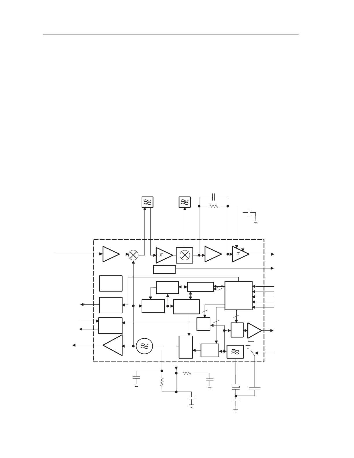
2.2 TRF6901 RF Block Diagram
Figure 2−1 shows the block diagram of the TRF6901 ISM transceiver IC.
Figure 2−1.TRF6901 Block Diagram
LNA_IN1, LNA_IN2
RF
IN
860 MHz to 930 MHz
DET_OUT
DC_DC_IN
DC_DC_OUT
PA_OUT
860 MHz to 930 MHz
typical 9 dBm
1, 2
45
25
22
4
LNA
Band-gap
Brownout
Detector
DC-DC
Converter
PA
Ceramic
IF Filter
Mixer
MIX_OUT
47
44, 43 35
/N
32/33
Ceramic
Discriminator
IF_IN1,2
Limiter
RSSI
/A-
Counter
CER_DIS
/Div. CTRL
/B-
Counter
PFD
CPs
15 CP_OUT13VCO_TUNE
LPF_IN
37 36
LPF Amplifier
Quad.
Dem.
8
6
8
/L
2..254
8
/Ref
2..255
LPF_OUT
LEARN/HOLD
39 34
Data Slicer
Serial
Interface
5
/K
2..62
30
XTAL
SLC_CAP
31
XTAL_SW
33
41
18
20
19
26
21
27
32
RX_DATA
RSSI_OUT
CLOCK
DATA
STROBE
STDBY
MODE
CLK_OUT
TX_DATA
2-2
Loop Filter
Page 17
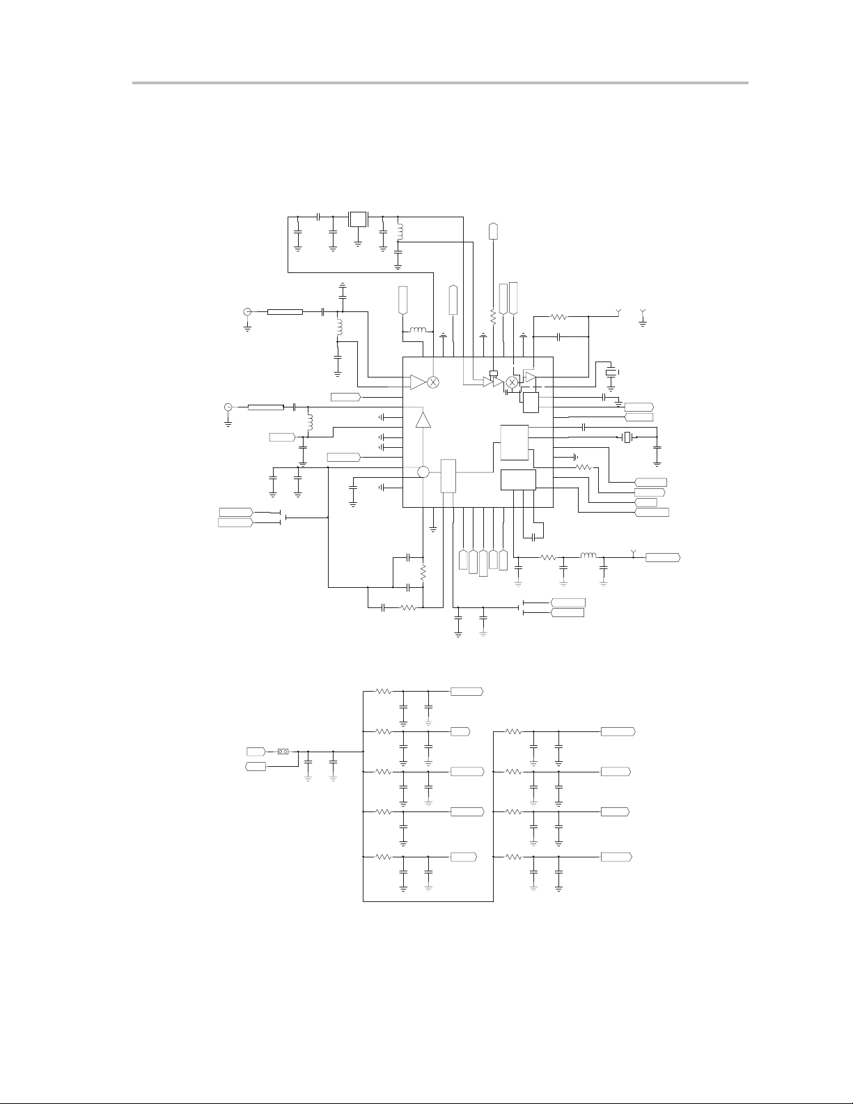
2.3 TRF6901 RF EVM Schematics
Figure 2−2 shows the TRF6901 RF EVM schematics.
Figure 2−2.TRF6901 RF EVM Schematics (1 of 4)
BPF1
SFECV10.7MA2S−A
BW=330kHz
C1
123
82pF
C3
C2
15pF
120pF
82pF
L1
C4
4.7 µH
C5
68pF
TRF6901 RF EVM Schematics
RSSI
C6
C13
150pF
22pF
L4
8.2 nH
C7
C9
2.7pF
LNA_VCC
VCO_VCC1
2.7pF
L2
10nH
PA_VCC
VCO_TANK2
VCO_TANK1
C18
100pF
VCO_VCC
C38
10000pF
1
2
3
4
5
6
7
8
9
10
11
12
C30
100pF
C37
1000pF
R13
6.8k
MIX_VCC
4.7uH
LNA
PA_OUT
L3
PA
VCO
VCO_TUNE
MIX_OUT
48
13
R10
18k
47
14
46
PLL
15
CP_OUT
DET_OUT
45
DET_OUT
CP_VCC
DVDD
C39
0.1uF
IF_IN1
44
TRF6901
TX OUT
RX_IN+
J2
VCO_VCC2
DCDC_OUT
50 OHM
TL1
J1
50 OHM
TL2
C11
1.8 pF
PA_V CC
C56
C17
10000pF
0.1uF
JP1
3
2
1
Figure 2−2. TRF6901 RF EVM Schematics (2 of 4)
VCC1
VCCM
R3
10
C15
0.1uF
R5
10
JP2
C23
C24
10000pF
0.1uF
C19
0.1uF
R7
10
C25
0.1uF
R11
10
C34
0.1uF
R14
0
C41
0.1uF
C16
10000pF
C20
10000pF
C26
10000pF
C42
10000pF
XTAL_VCC
DVDD
VCO_VCC1
VCO_VCC2
PA_V CC
IF_IN2
43
U1
181716
CLOCK
R1
RSSI
STROBE
0
42
C40
10000pF
RSSI_OUT
41
DATA
DEM_VCC
LRN/HOLD
40
Reference
generator
DC/DC
Conv.
212019
MODE
JP3
2
R6
10
R8
10
R12
10
R15
10
LEARN/HOLD
39
38
Data
slicer
CLK_OUT
C29
0.22uF
DC_DC_OUT
C31
0.47uF
3
1
37
LPF_IN
24C123C222
100
DNP
C21
0.1uF
C27
0.1uF
C35
0.1uF
C43
0.1uF
220k
82pF
R9
R2
C8
LPF_OUT
36
CER_DIS
35
SLC_CAP
34
RX_DATA
33
TX_DATA
32
31
30
XTAL
29
28
27
26
DC_DC_IN
25
C32
1.0uF
DNPDNP
DCDC_OUT
VCO_VCC2
C22
10000pF
C28
10000pF
C36
150pF
C44
10000pF
TP2
TP1
GND
LPF_OUT
LPF_OUT
DIS1
10.7
CDACV10M7GA001
C10
2200pF
RX_DAT A
XTAL_SW
DCDC_VCC
LNA_VCC
MIX_VCC
DEM_VCC
TX_DATA
XTAL1
20MHz
97SMX(C)−20MHZ
TP3
DCDC_OUT
C33
0.47uF
DNP
XTAL_VCC
MCU_CLK
STDBY
DCDC_VCC
DCDC_OUT
C14
15pF
C12
68pF
R4
0
L5
47uH
DNP
TRF6901 RF EVM PCB Hardware
2-3
Page 18
TRF6901 RF EVM Schematics
Figure 2−2. TRF6901 RF EVM Schematics (3 of 4)
VCC2
R16
220
LED1
ENABLE
LN1261C−(TR)
R19
Q1
FMMT2222ATA
TP14
EX_STDBY
VCC2
3 1
VCC2
R37
220
LED2
BRNOUT
LN1261C−(TR)
Q2
FMMT2222ATA
10k
R30
R29
10k
1.0k
JP5
VCC2
2
DB25M
VCC2
VCC2
R21
10k
U2
20
1
1OE
2
18
1A1
1Y1
4
16
1A2
1Y2
6
14
1A3
1Y3
8
12
1A4
1Y4
19
SN74LVT244BDW
2OE
11
2A192Y1
13
7
2A2
2Y2
15
5
2A3
2Y3
17
3
2A4
2Y4
10
P2
1
14
2
15
3
16
4
17
5
18
6
19
7
20
8
21
9
22
10
23
11
24
12
25
13
C47
0.1uF
TP6
CLOCK
TP7
DATA
TP8
STROBE
TP9
TXDATA
TP10
STDBY
TP11
MODE
TP12
LRNHOLD
TP16
BRNOUT
TP17
RXDATA
R20
100
R22
100
R23
100
R24
100
R25
100
R26
100
R27
100
TP13
EX_MODE
3 1
R28
1.0k
JP4
2
R38
10k
P1
103309−5
20
R17
VCCM
10
C45
0.1uF
R18
VCC2
10
C46
0.1uF
CR1
R36
R35
R34
R33
R32
R31
10k
10k
10k
R39
R40
10k
10k
10k
10k
10k
LL4148
12345678910111213141516171819
MCU_CLK
TP5
RSSI
RSSI
CLOCK
DATA
STROBE
TX_DATA
STDBY
MODE
LRN/HOLD
EXTERNAL_TX_DATA
DET_OUT
RX_DAT A
MCU_CLK
RSSI
CLOCK
DATA
STROBE
TX_DATA
STDBY
MODE
LRN/HOLD
TP15
EX_TXDATA
DET_OUT
RX_DAT A
Figure 2−2. TRF6901 RF EVM Schematics (4 of 4)
POWER
TP4
6 V min to 8 V max
TP18
GND
ZR1
SMBJ8.5CA
C49
10uF
C50
0.1uF
VR1
REG101NA−A
1
IN
3
EN
GND
C52
0.1uF
VR2
REG101NA−3.3
1
IN
3
EN
GND
C55
0.1uF
2
2
OUT
ADJ
OUT
NR
5
4
CCWCW
W
5
4
C54
10000pF
R41
1.8k
R43
5k
R45
820
C48
10000pF
C53
10uF
C51
10uF
R42
1.8−3.6V(3.0VTYP)
0
1
JP6
2
LED3
VCC1
LN1261C−(TR)
R44
220
VCC1
3.3V
VCC2
2-4
Page 19
2.4 Top- and Bottom-Side Silkscreen and Drawing
Figure 2−3 shows the top-side silkscreen of the TRF6901 RF EVM and
Figure 2−4 shows the bottom-side silkscreen.
Figure 2−3.Top-Side Silkscreen and Drawing of TRF6901
TRF6901 RF EVM Schematics
Figure 2−4.Bottom-Side Silkscreen of TRF6901 RF EVM
TRF6901 RF EVM PCB Hardware
2-5
Page 20

Parts List
Murata SFECV10.7MA2S−A−TC Murata
SFECV10.7MA
2S−A−TC
Piezoelectric ceramics
SFECV10.7 Surface mounted chip
330 kHz
Murata GRM39X7R104J016AD Murata
4J016AD
filters for AM and FM
applications
Murata GRM39X7R224J010AD Murata
4J010AD
Murata GRM39Y5V474J010AD Murata
4J010AD
Murata GRM39Y5V105J010AD Murata
5J010AD
Murata GRM39C02R2C050AD Murata
C050AD
Murata GRM39C02R7C050AD Murata
C050AD
Murata GRM235Y5V106Z016AD Murata
GRM235Y5V1
Murata GRM39C0150J050AD Murata
06Z016AD
capacitor—tantalum
J050AD
replacement
Murata GRM39C0220J050AD Murata
J050AD
Murata GRM39C0680J050AD Murata
J050AD
Murata GRM39C0820J050AD Murata
J050AD
2.5 Parts List
2-6
RefDes Value Note Pattern Name Description Part Number Manufacturer Distributor P/N Distributor
Count
1 BPF1 BW =
0.1 µF 0603 Ceramic chip capacitor GRM39X7R10
C19, C21,
C23, C25,
C27, C34,
C35, C39,
18 C15, C17,
C41, C43,
C45−C47,
C50, C52,
C55
1 C29 0.22 µF 0603 Ceramic chip capacitor GRM39X7R22
2 C31, C33 0.47 µF DNP 0603 Ceramic chip capacitor GRM39Y5V47
1 C32 1 µF DNP 0603 Ceramic chip capacitor GRM39Y5V10
1 C11 1.8 pF 0603 Ceramic chip capacitor GRM39C02R2
2 C6, C9 2.7 pF 0603 Ceramic chip capacitor GRM39C02R7
10 µF 1210 Monolithic chip
C53
3 C49, C51,
2 C2, C14 15 pF 0603 Ceramic chip capacitor GRM39C0150
1 C7 22 pF 0603 Ceramic chip capacitor GRM39C0220
2 C5, C12 68 pF 0603 Ceramic chip capacitor GRM39C0680
3 C1, C3, C8 82 pF 0603 Ceramic chip capacitor GRM39C0820
Page 21

DistributorDistributor P/NManufacturerPart NumberDescriptionPattern NameNoteValueRefDes
Murata GRM39C0101J050AD Murata
Murata GRM39C0121J050AD Murata
Murata GRM39C0151J050AD Murata
Murata GRM39X7R102J050AD Murata
Murata GRM39X7R222J050AD Murata
Murata GRM39X7R103J050AD Murata
90F2624 Newark
Components
Murata LQG21C4R7N00T1 Murata
Murata LQW1608A8N2D00 Murata
Parts List
Murata LQW1608A10NJ00T1 Murata
J050AD
J050AD
J050AD
2J050AD
2J050AD
3J050AD
10000 pF 0603 Ceramic chip capacitor GRM39X7R10
142−0701−801 Johnson
− horizontal/PC mount
0.062 Thk
00T1
2D00
NJ00T1
S1812−473K API Delevan DN1132TR−ND Digi-Key
LN1261C−(TR) Panasonic P503TR−ND Digi-Key
(Shielded)
LED-gull wing-GW
LED, GW type Surface mount
ENABLE
BRNOUT
Type-Red
VCC1
Count
2 C18, C30 100 pF 0603 Ceramic chip capacitor GRM39C0101
1 C4 120 pF 0603 Ceramic chip capacitor GRM39C0121
2 C13, C36 150 pF 0603 Ceramic chip capacitor GRM39C0151
1 C37 1000 pF 0603 Ceramic chip capacitor GRM39X7R10
1 C10 2200 pF 0603 Ceramic chip capacitor GRM39X7R22
C22, C24,
C26, C28,
13 C16, C20,
C38, C40,
C42, C44,
C48, C54,
C56
1 CR1 MELF3 (MINIMELF) Fast switching diode LL4148 Diode INC LL4148CT−ND Digi-Key
2 J1, J2 SMA_H SMA brass connector
2 JP1, JP3 SMD−3 way-JP Jumper-3 Way-SMD
2 JP2, JP6 Jumper-2 pin Breakaway headers 4−103239−0 AMP 90F7725 Newark
2 JP4, JP5 Jumper-3 pin Breakaway headers 4−103239−0 AMP 90F7725 Newark
2 L1, L3 4.7 µH 0805−Murata Chip inductor LQG21C4R7N
TRF6901 RF EVM PCB Hardware
1 L4 8.2 nH 0603 Chip inductor LQW1608A8N
1 L2 10 nH 0603 Chip inductor LQW1608A10
LED2,
1 L5 47 µH DNP 0805−1812 Chip inductor
3 LED1,
2-7
LED3
Page 22

Parts List
DistributorDistributor P/NManufacturerPart NumberDescriptionPattern NameNoteValueRefDes
Venkel CR0603−16W−000T Venkel
Venkel CR0603−16W−102JT Venkel
Venkel CR0603−16W−182JT Venkel
Venkel CR0603−16W−682JT Venkel
Venkel CR0603−16W−100JT Venkel
Venkel CR0603−16W−103JT Venkel
Venkel CR0603−16W−183JT Venkel
Venkel CR0603−16W−183JT Venkel
Venkel CR0603−16W−101JT Venkel
Venkel CR0603−16W−221JT Venkel
Venkel CR0603−16W−224JT Venkel
Venkel CR0603−16W−821JT Venkel
Murata CDACV10M7GA001−R0 Murata
97B3257 Newark
Corp.
97B3259 Newark
Corp.
000T
102JT
0 Ω 0603 Chip resistor CR0603−16W−
182JT
3296W−1−XXX Bourns 3296W−XXX−ND Digi-Key
trimming potentiometer
682JT
100JT
10 Ω 0603 Chip resistor CR0603−16W−
103JT
10 kΩ 0603 Chip resistor CR0603−16W−
183JT
183JT
101JT
100 Ω 0603 Chip resistor CR0603−16W−
221JT
224JT
220 Ω 0603 Chip resistor CR0603−16W−
821JT
CDACV10M7G
A001−R0
for FM receiver
TP−105−01−02 Components
TP−105−01−00 Components
point (Red)
point (Black)
2-8
Count
4 R1, R4,
R14, R42
2 R28, R29 1 kΩ 0603 Chip resistor CR0603−16W−
1 R41 1.8 kΩ 0603 Chip resistor CR0603−16W−
1 R43 5 kΩ 3296W Bourns 3/8-inch square
R11, R12,
R15, R17,
1 R13 6.8 kΩ 0603 Chip resistor CR0603−16W−
10 R3, R5−R8,
R18
12 R19, R21,
R30−R36,
R38−R40
1 R10 18 kΩ 0603 Chip resistor CR0603−16W−
R22−R27
1 R9 100 Ω DNP 0603 Chip resistor CR0603−16W−
7 R20,
R44
3 R16, R37,
1 R2 220 kΩ 0603 Chip resistor CR0603−16W−
1 R45 820 Ω 0603 Chip resistor CR0603−16W−
1 DIS1 10.7 MHz CDACV Type Ceramic discriminator
1 TP4 P.C. test point Color coded P.C. test
2 TP2, TP18 GND P.C. test point Color coded P.C. test
Page 23

DistributorDistributor P/NManufacturerPart NumberDescriptionPattern NameNoteValueRefDes
97B3253 Newark
Corp.
97B3253 Newark
Corp.
97B3253 Newark
Corp.
97B3253 Newark
Corp.
97B3253 Newark
Corp.
97B3253 Newark
Corp.
97B3253 Newark
Corp.
97B3253 Newark
Corp.
97B3253 Newark
Corp.
97B3253 Newark
Corp.
97B3253 Newark
Corp.
97B3253 Newark
Corp.
97B3253 Newark
Corp.
97B3253 Newark
Corp.
Parts List
97B3253 Newark
Corp.
TP−105−01−09 Components
TP−105−01−09 Components
point (White)
point (White)
TP−105−01−09 Components
TP−105−01−09 Components
point (White)
point (White)
TP−105−01−09 Components
TP−105−01−09 Components
point (White)
point (White)
TP−105−01−09 Components
TP−105−01−09 Components
point (White)
point (White)
TP−105−01−09 Components
TP−105−01−09 Components
point (White)
point (White)
TP−105−01−09 Components
TP−105−01−09 Components
point (White)
point (White)
TP−105−01−09 Components
TP−105−01−09 Components
point (White)
point (White)
TP−105−01−09 Components
103309−5 AMP A26274−ND Digi-Key
point (White)
header assembly
747238−4 AMP A2098−ND Digi-Key
connector-25 pin-right
angle-male
Count
15 TP16 BRNOUT P.C. test point Color coded P.C. test
TP6 CLOCK P.C. test point Color coded P.C. test
TP7 DATA P.C. test point Color coded P.C. test
TP3 DCDC_OUT P.C. test point Color coded P.C. test
TP13 EX_MODE P.C. test point Color coded P.C. test
TP14 EX_STDBY P.C. test point Color coded P.C. test
TP15 EX_TXDATA P.C. test point Color coded P.C. test
TP1 LPF_OUT P.C. test point Color coded P.C. test
TP12 LRNHOLD P.C. test point Color coded P.C. test
TP11 MODE P.C. test point Color coded P.C. test
TP5 RSSI P.C. test point Color coded P.C. test
TP17 RXDATA P.C. test point Color coded P.C. test
TP10 STDBY P.C. test point Color coded P.C. test
TP8 STROBE P.C. test point Color coded P.C. test
TRF6901 RF EVM PCB Hardware
TP9 TXDATA P.C. test point Color coded P.C. test
1 P1 103309−5 Amp−latch low profile
1 P2 DB25M Subminiature D
2-9
Page 24

Parts List
DistributorDistributor P/NManufacturerPart NumberDescriptionPattern NameNoteValueRefDes
Zetex FMMT2222ACT−ND Digi-Key
FMMT2222AT
A
Digi-Key
Instruments
296−1707−5−ND Digi-Key
Texas
Instruments
SN74LVT244B
DW
REG101NA−A Burr−Brown REG101NA−A−ND Digi-Key
Burr−Brown REG101NA−3.3−ND Digi-Key
REG101NA−3.
3
SMBJ8.5CA Vishay/Liteon SMBJ8.5AGICT−ND Digi-Key
97B2647 Newark
Corp.
TP−107−01 Components
transistor − 330 mW
Count
2 Q1, Q2 SOT23 NPN switching
1 U1 TQFP48 Transceiver TRF6901 Texas
drivers with 3-state
outputs
regulator
1 U2 SO20WB Octal buffers and line
1 VR1 SOT23−5 100-mA low-dropout
regulator
1 VR2 SOT23−5 100-mA low-dropout
1 XTAL1 20 MHz 97SMX(C) Quartz crystal 97M200−20(C) SMI 97M200−20(C) SMI
suppressor
1 XTAL1A 20 MHz DNP 93SMX Quartz crystal 93M200−20 SMI 93M200−20 SMI
1 ZR1 SMBJ−BI Transient voltage
point
SMD test point Surface mount test
GND3
2 GND2,
2-10
Page 25
TRF6901 RF EVM Regulated Supply Configuration
V
for REG101NA Regulator is Equal to:
2.6 TRF6901 RF EVM Regulated Supply Configuration
The evaluation board should be used with a dc power supply voltage of 6 V
to 8 V nominal. Figure 2−5 details the dc voltage supply setup for the TRF6901
RF-only EVM.
There are three powering sources on the TRF6901 and the EVM. The
adjustable output VCC1 powers all the blocks of the TRF6901 IC. The fixed
output VCC2 powers all the components external to the TRF6901, such as
LEDs and the digital I/O portions of the EVM. This separation of sources
eliminates noise and other potential interferences. The third source is a dc-dc
converter which is internal to the TRF6901 IC. The dc-dc converter can
provide an adequate voltage to the charge pumps and VCO core in the event
an external power supply, such as a battery, drops down to 1.8 V. Hence,
increasing the operational period of the TRF6901.
VCC1 output branches out into VCO_VCC1, VCO_VCC2, XTAL_VCC,
DVDD, PA_VCC, DCDC_VCC, LNA_VCC, MIX_VCC, and DEM_VCC when
JP2 (see Jumper Description) is connected. These are utilized in powering
various blocks of the TRF6901 IC. Prior to using the RF EVM, ensure that
VCC1 is set to the nominal voltage of approximately 3 V by adjusting R43, if
necessary.
Figure 2−5.TRF6901 EVM DC Voltage Setup
OUT
V
= 1.267 [1+(R41/R43)]
OUT
V at Terminal 1 of REG101NA Should Be 2 V
to 3 V Higher Than V
VR1
REG101NA−A
1
IN
3
C52
0.1 uF
1
3
C55
0.1uF
OUT
EN
ADJ
GND
2
VR2
REG101NA−3.3
IN
OUT
EN
NR
GND
2
POWER
TP4
6 V to 8 V
TP18
GND
ZR1
SMBJ8.5CA
VIN is
6 V min to
8 V max
C49
10 uF
C50
0.1 uF
5
4
5
4
OUT
CCWCW
W
C54
10000 pF
R41
1.8k
R43
5k
R45
820
C48
10000 pF
C53
10 uF
VCC1 is Nominally 3 V
R42
1.8 V to 3.6 V (3 V TYP)
0
C51
10 uF
V
Used to Change V
adj
From 1.8 V to 3.6 V
1
JP6
Connected JP6 for
2
Power on LED
LED3
VCC1
LN1261C−(TR)
R44
220
OUT
VCC1
3.3 V
VCC2
2-11
Page 26
TRF6901 Parallel Port Module Interface
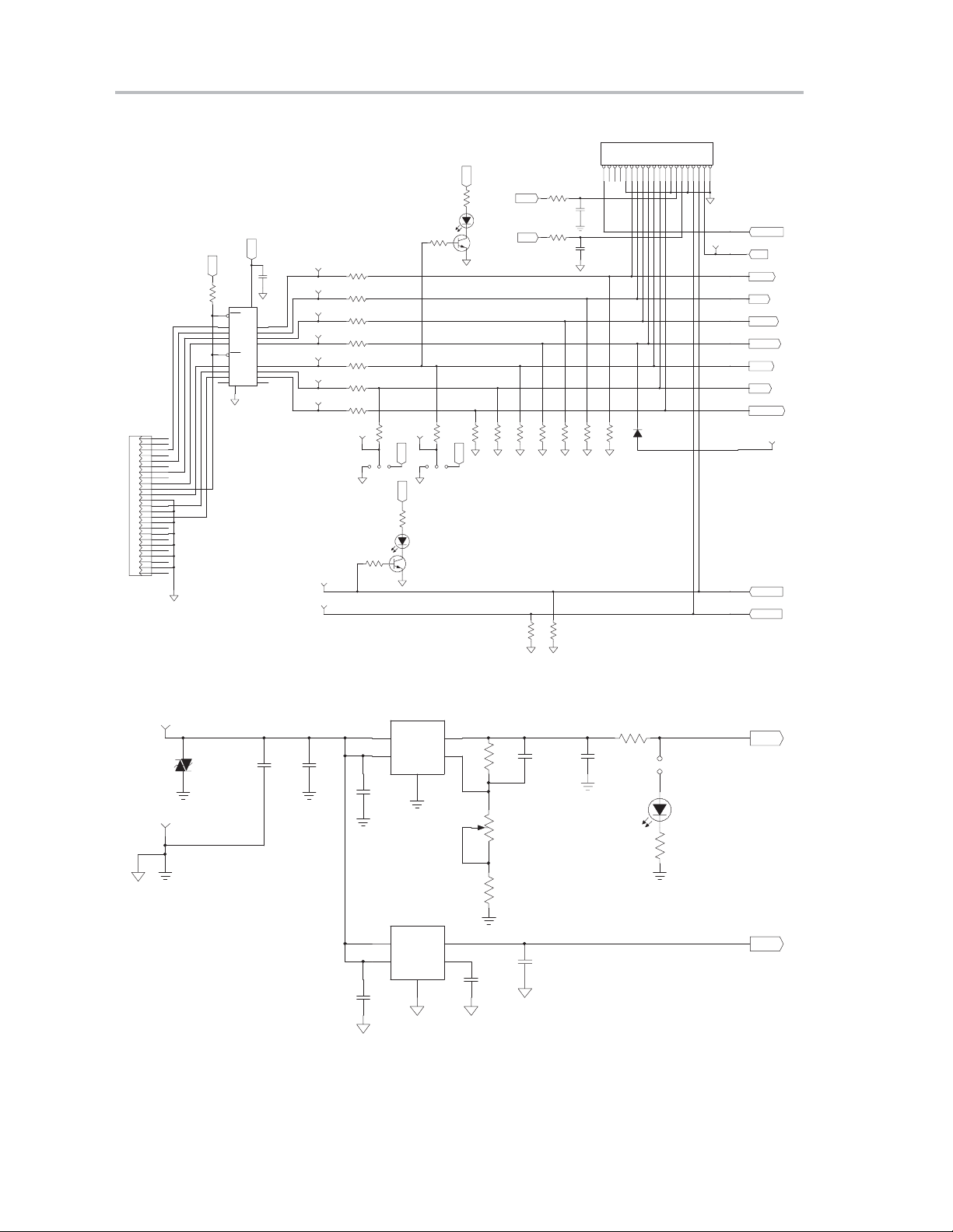
2.7 TRF6901 Parallel Port Module Interface
Figure 2−6 details the parallel port interface portion of the TRF6901 RF EVM.
Figure 2−6.TRF6901 RF EVM Parallel Port Interface
VCC2
R16
220
LED1
ENABLE
LN1261C−(TR)
R19
Q1
FMMT2222ATA
TP14
EX_STDBY
VCC2
3 1
VCC2
R37
220
LED2
BRNOUT
LN1261C−(TR)
Q2
FMMT2222ATA
10k
R30
R29
10k
1.0k
JP5
VCC2
2
DB25M
VCC2
VCC2
R21
10k
U2
20
1
1OE
2
18
1A1
1Y1
4
16
1A2
1Y2
6
14
1A3
1Y3
8
12
1A4
1Y4
19
SN74LVT244BDW
2OE
11
2A192Y1
13
7
2A2
2Y2
15
5
2A3
2Y3
17
3
2A4
2Y4
10
P2
1
14
2
15
3
16
4
17
5
18
6
19
7
20
8
21
9
22
10
23
11
24
12
25
13
C47
0.1uF
TP6
CLOCK
TP7
DATA
TP8
STROBE
TP9
TXDATA
TP10
STDBY
TP11
MODE
TP12
LRNHOLD
TP16
BRNOUT
TP17
RXDATA
R20
100
R22
100
R23
100
R24
100
R25
100
R26
100
R27
100
TP13
EX_MODE
3 1
R28
1.0k
JP4
2
R38
10k
P1
103309−5
20
R17
VCCM
10
C45
0.1uF
R18
VCC2
10
C46
0.1uF
CR1
R36
R35
R34
R33
R32
R31
10k
10k
10k
R39
R40
10k
10k
10k
10k
10k
LL4148
12345678910111213141516171819
MCU_CLK
TP5
RSSI
RSSI
CLOCK
DATA
STROBE
TX_DATA
STDBY
MODE
LRN/HOLD
EXTERNAL_TX_DATA
DET_OUT
RX_DAT A
MCU_CLK
RSSI
CLOCK
DATA
STROBE
TX_DATA
STDBY
MODE
LRN/HOLD
TP15
EX_TXDATA
DET_OUT
RX_DAT A
2-12
Page 27
TRF6901 RF EVM Jumpers
2.8 TRF6901 RF EVM Jumpers
2.8.1 Jumper Connections
Figure 2−7 shows the default position of the jumpers on the TRF6901 RF EVM.
Figure 2−7. TRF6901 RF EVM Jumper Locations and Default Configurations of the
EVM (Sheet 1 of 2)
BPF1
SFECV10.7MA2S−A
BW=330kHz
C1
1
3
C2
15pF
82pF
C3
82pF
C4
2
120pF
L1
4.7 uH
C5
68pF
RSSI
TX OUT
RX_IN+
J2
VCO_VCC2
DCDC_OUT
C6
50OHM
50OHM
C17
0.1uF
TL2
PA_VCC
3
1
TL1
JP1
C11
1.8 pF
2
C13
150pF
C56
10000pF
J1
C7
22pF
L4
8.2 nH
2.7pF
L2
10nH
C9
2.7pF
LNA_VCC
VCO_VCC1
PA_VCC
VCO_VCC
VCO_TANK2
VCO_TANK1
C18
100pF
10000pF
C38
1
2
3
4
5
6
7
8
9
10
11
12
100pF
1000pF
MIX_VCC
L3
4.7uH
LNA
PA_OUT
C30
C37
R13
6.8k
MIX_OUT
48
PA
VCO
VCO_TUNE
13
R10
18k
47
14
46
PLL
15
CP_OUT
DET_OUT
IF_IN1
45
44
DET_OUT
TRF6901
17
16
CP_VCC
DVDD
C39
0.1uF
R1
IF_IN2
43
RSSI
U1
18
CLOCK
0
RSSI_OUT
42
41
Reference
Generator
20
19
DATA
STROBE
C40
10000pF
DEM_VCC
LRN/HOLD
LEARN/HOLD
40
39
DC/DC
Conv.
21
DC_DC_OUT
MODE
JP3
2
38
Data
Slicer
CLK_OUT
C29
0.22uF
C31
0.47uF
DNP
3
1
37
LPF_IN
24C123C222
R9
100
DNP
R2
220k
C8
82pF
LPF_OUT
36
CER_RES
35
SLC_CAP
34
RX_DATA
33
TX_DAT A
32
31
30
XTAL
29
28
27
26
DC_DC_IN
25
C32
1.0uF
DNP
DCDC_OUT
VCO_VCC2
C12
R4
0
LPF_OUT
XTAL_SW
68pF
L5
47uH
DNP
C10
2200pF
TP2
TP1
GND
LPF_OUT
RES1
10.7
CDACV10M7GA001
RX_DAT A
TX_DATA
XTAL1
20MHz
97SMX(C)−20MHZ
XTAL_VCC
MCU_CLK
STDBY
DCDC_VCC
TP3
DCDC_OUT
C33
0.47uF
DNP
C14
15pF
DCDC_OUT
2-13
Page 28

TRF6901 RF EVM Jumpers
POWER
Figure 2−7. TRF6901 RF EVM Jumper Locations and Default Configurations of the
EVM (Sheet 2 of 2)
TP4
6.0V_TO_8.0V
TP18
GND
ZR1
SMBJ8.5CA
C49
10uF
C50
0.1uF
REG101NA−A
1
3
C52
0.1uF
REG101NA−3.3
1
3
C55
0.1uF
R3
10
VR1
R42
1.8 −3.6V (3.0V TYP)
0
1
JP6
2
LED3
VCC1
LN1261C−(TR)
R44
220
VCC1
3.3V
VCC2
GND
VR2
GND
C15
0.1uF
2
2
OUT
ADJ
OUT
NR
5
4
5
4
C16
10000pF
R41
1.8k
CCWCW
R43
W
R45
820
C54
10000pF
XTAL_VCC
C48
10000pF
5k
C53
10uF
C51
10uF
IN
EN
IN
EN
VCC1
VCCM
JP2
C23
0.1uF
C24
10000pF
R5
10
R7
10
R11
10
R14
DVDD
C19
C20
0.1uF
10000pF
VCO_VCC1
C25
C26
0.1uF
10000pF
VCO_VCC2
C34
0.1uF
0
C41
0.1uF
C42
10000pF
PA_VCC
R6
10
R8
10
R12
10
R15
10
C21
0.1uF
C27
0.1uF
C35
0.1uF
C43
0.1uF
C22
10000pF
C28
10000pF
C36
150pF
C44
10000pF
DCDC_VCC
LNA_VCC
MIX_VCC
DEM_VCC
2-14
Page 29

2.8.2 Default Jumper Connections
TRF6901 RF EVM Jumpers
JP1
JP3
1
2
3
JP5
1
2
3
JP2
1
2
3
To U1−22 DC_DC_OUT
To U1−10 VCO_TANK2
To VCO_VCC2
1
2
To VCC1
To VCCM
JP4
To VCO_VCC2
To U1−16 CP_VCC
To U1−22 DC_DC_OUT
1
2
3
JP4 Default is no connection
To VCC2
To U1−21 MODE
To GND
JP6
To VCC2
1
To U1−26 STDBY
2
To GND
To VCC1
To LED3
JP5 Default is no connection
2.8.3 Jumper Description
The jumpers on the TRF6901 RF-only EVM, as shown in Figure 2−7, are used
for the following purposes.
- JP1
This jumper selects one source that is either VCO_VCC2 or DC_DC_OUT
for the VCO. When JP1−3 is connected to JP1−2, VCO_VCC2 is fed to the
VCO. If JP1−2 is connected to JP1−1, DCDC_OUT is connected to the
VCO. The default connection is JP1−3 to JP1−2.
- JP2
This jumper connects VCC1 input to VCCM. It also connects VCC1 input
to filtering networks that lead to various outputs such as XTAL_VCC,
DVDD, VCO_VCC1, VCO_VCC2, and PA_VCC. These are then used to
power various blocks of the TRF6901 IC. An advantage of using this
jumper is that when removed, the two disconnected nodes can be
connected through an ammeter that allows the user to measure the
Denotes Default Connection
2-15
Page 30

Connectors
current consumption. Also, the user can insert a power supply after the
REG101NA voltage regulators. Since there is no regulation stage after
this jumper, make sure that any supply connected to this jumper is noise
free and is set between 1.8 V and 3.6 V.
- JP3
This jumper connects one source that is either VCC_VCC2 or
DC_DC_OUT to the charge pumps of the phase lock loop. When JP3−1 is
connected to JP3−2, VCO_VCC2 is fed to the charge pumps of the PLL
through terminal U1−16 CP_VCC. If JP3−2 is connected to JP3−3,
DCDC_OUT is connected to the charge pumps. The default connection is
JP3−2 to JP3−1.
- JP4
This jumper either acts as a pullup or a pulldown for the MODE terminal.
When JP4−1 is connected to JP4−2, then R28 acts as a pullup resistor . O n
the other hand, when JP4−2 is connected to JP4−3, then R28 acts as a
pulldown resistor. The default configuration for JP4 is no connection.
- JP5
2.9 Connectors
This jumper either acts as a pullup or a pulldown for the STDBY terminal.
When JP5−1 is connected to JP5−2, then R29 acts as a pullup resistor . O n
the other hand, when JP5−2 is connected to JP5−3, then R29 acts as a
pulldown resistor. The default configuration for JP5 is no connection.
- JP6
This jumper connects the VCC1 regulated power output to LED3 when
JP6−1 is connected to JP6−2. This LED verifies EVM dc voltage is applied.
The following are descriptions of the TRF6901 EVM connectors and test
points.
- P1
P1 is a 20-terminal connector that is used to connect to an external
microprocessor or DSP that provides the DATA, CLOCK, STROBE,
TX_DATA, STDBY, MODE, and LRN/HOLD inputs to the TRF6901. In this
case, the TRF6901 is controlled by an external microprocessor or DSP
rather than the control software on the PC. This port also connects to the
serial port module that contains the MSP430F149 via a 20-pin cable. P1
can also be used to interface directly to the TRF6901, bypassing the
parallel port interface circuitry on the EVM.
2-16
- P2
P2 is the PC parallel port interface and is a male DB25 connector. P2 is
connected to the LPT1 or LPT2 port of the computer on which the control
software of TRF6901 is running.
Page 31

-
- J2 TX_OUT
2.10 Test Points (TP)
- LPF_OUT TP1
- GND TP2 and TP18
- DCDC_OUT TP3
Test Points (TP)
J1 RX_IN+
J1 RX_IN+ is an SMA female connector that feeds the received signal into
the input of the LNA.
J2 TX_OUT is an SMA female connector which is connected to the
transmitter output of the TRF6901.
The LPF_OUT test point is used to monitor the output signal of the LPF
stage before passing through the data slicer.
These test points are used for ground connections.
The DCDC_OUT test point is used to monitor the DCDC_OUT signal from
U1−22 DC_DC_OUT terminal.
- POWER TP4
This test point is used to connect the output voltage of the power supply to
the TRF6901 RF EVM. The nominal values for the external power supply
are from 6 V to 8 V.
- RSSI TP5
The RSSI test point is used to monitor the RSSI level from U1−41
RSSI_OUT terminal.
- CLOCK TP6
The CLOCK test point is used to monitor the clock signal from the PC
parallel port (P2) that connects to U1−18 CLOCK terminal.
- DATA TP7
The DATA test point is used to monitor the DATA signal from the PC
parallel port (P2) i.e., the words (see Chapter 3, TRF6901 RF EVM Control
Software) sent from the control software of TRF6901. This test point
connects to U1−20 DATA terminal.
- STROBE TP8
The STROBE test point is used to monitor the STROBE signal from the PC
parallel port (P2). This test point connects to U1−19 STROBE terminal.
- TXDATA TP9
The TXDATA test point is used to monitor the transmitted data coming
from PC parallel port (P2). This test point connects to U1−32 TX_DATA
terminal.
2-17
Page 32

Adjustments
STDBY TP10
-
The STDBY test point is used to monitor the STDBY signal from the PC
parallel port (P2). This test point connects to U1−26 STDBY terminal.
- MODE TP11
The MODE test point is used to monitor the MODE signal from the PC
parallel port (P2). This test point connects to U1−21 MODE terminal.
- LRNHOLD TP12
The LRNHOLD test point is used to monitor the LRNHOLD signal from the
PC parallel port (P2). This signal determines whether the TRF6901 is in
LEARN mode or HOLD mode. This test point connects to U1−39
LEARN/HOLD terminal.
- EX_MODE TP13
The EX_MODE test point allows inputting the MODE signal externally
from another source into U1−21 MODE terminal.
- EX_STDBY TP14
The EX_STDBY test point allows inputting the STDBY signal externally
from another source into U1−26 STDBY terminal.
2.11 Adjustments
- EX_TXDATA TP15
The EX_TXDATA TP is used to inject data from an external source into
U1−32 TX_DATA terminal. This test point is utilized during the FSK
modulation and transmitter test (see Chapter 3, TRF6901 RF EVM Control
Software).
- BRNOUT TP16
The BRNOUT test point is used to monitor the signal from U1−45
DET_OUT terminal. This signal indicates whether the brownout detector
is activated.
- RXDATA TP17
The RXDATA test point is used to monitor the received data from U1−33
RX_DATA. This test point is used during the receiver testing (see
Chapter 3, TRF6901 RF EVM Control Software).
Resistor R43 is varied to adjust the VCC1 voltage applied to U1 (TRF6901).
2-18
Page 33

2.12 LED Indicators
LED Indicators
- VCC1 LED3
If JP6 is installed, the VCC LED is illuminated when voltage is applied to
U1.
- ENABLE LED1
The ENABLE LED is illuminated when the STDBY line from computer is in
a high state. The STDBY line is in a high state when the TRF6901 is
commanded to STDBY.
- BRNOUT LED2
Indicates whether the brownout detector is activated.
2-19
Page 34

2-20
Page 35

Chapter 3
"#
This chapter describes the installation and use of the TRF6901 RF EVM
control software. The features and functionality of this tool are described.
Topic Page
3.1 TRF6901 RF EVM Control Software Overview 3-2. . . . . . . . . . . . . . . . . . .
3.2 TRF6901 RF EVM Control Software Installation 3-2. . . . . . . . . . . . . . . . . .
3.3 TRF6901 RF EVM Setup With Control Software 3-2. . . . . . . . . . . . . . . . . .
3.4 How to Use the TRF6901 Control Software 3-3. . . . . . . . . . . . . . . . . . . . . .
3.5 Main Program Screen 3-3. . . . . . . . . . . . . . . . . . . . . . . . . . . . . . . . . . . . . . . . .
3.6 IC Layout Screen 3-10. . . . . . . . . . . . . . . . . . . . . . . . . . . . . . . . . . . . . . . . . . . . .
3.7 Testing the Transmitter 3-13. . . . . . . . . . . . . . . . . . . . . . . . . . . . . . . . . . . . . . .
3.8 Testing of the Receiver 3-20. . . . . . . . . . . . . . . . . . . . . . . . . . . . . . . . . . . . . . .
TRF6901 RF EVM Control Software
3-1
Page 36

TRF6901 RF EVM Control Software Overview
3.1 TRF6901 RF EVM Control Software Overview
The TRF6901 comes with control software that is designed to control the
TRF6901 EVM ISM-band transceiver IC by PC via the parallel port. This
software is a Windows-based GUI interface that allows the user to control
different components and settings of the transmitter and receiver. This
software also has the capability of running an FSK test. This software is an
effective tool for evaluating the TRF6901. The user can connect measuring
and testing equipment to the TRF6901 EVM and use this software to observe
different parameters and features of the TRF6901.
3.2 TRF6901 RF EVM Control Software Installation
The software is intended for use in either a Windows 95/98 or Windows
NT/2000 environment. The IOPort.sys driver is needed for computers running
either Windows NT or Windows 2000 operating system. The user must put the
IOPort.sys driver in the directory c:\WINNT\system32\drivers
write to the parallel port. However, if the operating system is Windows 95/98,
the software application can run on its own.
Both the Windows NT/2000 Driver and the TRF6901 software are provided on
disk. Your system administrator must install the Windows NT/2000 driver if you
do not have administrative rights to the computer. The TRF6901 can run from
the floppy disk by following these steps:
in order to
1) Click on the Start Button on the desktop.
2) Click on the Run button.
3) Type A:\ TRF6901.exe and press OK.
Or you can:
1) Open the My Computer icon on the desktop.
2) Open the A:\ directory.
3) Right click on TRF6901.exe.
4) Paste TRF6901.exe onto the desktop.
Note:
This software is available on the CD ROM and a floppy diskette.
3.3 TRF6901 RF EVM Setup With Control Software
The 3.5-inch diskette supplied with the TRF6901 contains the control software
required to demonstrate the TRF6901. Complete the following steps to set up
the TRF6901 for evaluation.
3-2
1) Place the 3.5-inch diskette into the floppy disk drive of the computer being
used to evaluate the TRF6901.
Page 37

2) Follow the installation instructions described in TRF6901 RF EVM Control
Software Installation.
3) Connect a DB25 female to DB25 male cable between the TRF6901
evaluation board and the PC parallel port. The DB25 female end of the
cable is connected to the TRF6901. The DB25 male end of the cable is
connected to the desired LPT port of the PC (LPT1 or LPT2).
4) Connect a dc power supply capable of 8 V 200 mA between the red power
supply terminal and ground on the TRF6901 evaluation board.
5) Verify that the power supply output is set between 6 V and 8 V.
6) Turn the power supply on.
7) If the jumper at JP6 is installed, verify that LED3 (the red power-on LED)
is illuminated.
8) Run the TRF6901.exe file on the PC.
9) Press the Send All Words (F7) button on the program screen.
3.4 How to Use the TRF6901 Control Software
How to Use the TRF6901 Control Software
The main program screen appears when you open the TRF6901.exe file. The
TRF6901 control software has two screens, the main program screen, and the
IC layout screen. The main program screen and the IC layout screen offer the
same functionality, with the only major difference being that the IC layout
screen is a replica of the TRF6901 block diagram.
3.5 Main Program Screen
The main program screen is divided into six main parts: Synthesizer, Mode
Options, Operating Modes, Help, Words, and Operation Mode. All the fields
in each section can be changed either by typing in the box or by double
clicking it.
TRF6901 RF EVM Control Software
3-3
Page 38

Main Program Screen
Figure 3−1.Main Program Screen
Transmit Frequency for Transmit
Mode or LO Frequency for Receive
Crystal or Clock Frequency
Output
Frequency Set
Reference
Divider Set
Crystal Reference Divide
dc-dc Clock Divider
Buffer Clock Divider
dc-dc Clock Divider Set
Buffer Clock Divider Set
Double Click Here With the
Left Mouse Button to Obtain
the IC Layout Form
Note: When words are displayed in RED, it indicates that you need to send the change to the TRF6901. Pressing the Word A, B,
C, D, or the Send All Words Button sends the update to the TRF6901.
3.5.1 Synthesizer
The following is a brief summary of the controls in this section.
- Output Frequency {Desired Freq.}
Sets the output frequency to the value typed inside the field. In transmit
mode, the desired frequency is the frequency of the signal transmitted out
of the P A. In receive mode the desired frequency is the LO frequency for
the mixer. The appropriate frequency range for TRF6901 is 860 MHz to
930 MHz.
Note:
This field is used with the Set button right below the box. Press the Set button
before clicking Send Words to make sure that the entry is valid.
- Output Frequency Set Button {Set} (Beside Divide by-N field)
This button checks the frequency entered by the user to make sure that it is
a multiple integer of the reference frequency. Click this button after
3-4
Page 39

Main Program Screen
entering the des i r e d frequency. If the entered frequency is not a multiple of
the reference frequency, then it is rounded down to the closest frequency
that satisfies this requirement.
- Feedback Divider {Div−by N}
The software calculates the feedback divider from the desired frequency,
crystal clock frequency, and the reference divider value of the integer-N
PLL. This field cannot be edited.
- Crystal Frequency {Crystal Freq.}
The default crystal installed on the TRF6901 RF EVM board is 20 MHz,
hence the default value for this field is 20 MHz. It can be varied from 10
MHz to 20 MHz. For example, if the user removes the 20-MHz crystal and
instead installs a 15-MHz crystal on the TRF6901 RF EVM, then the
frequency entered in this field should be 15 MHz.
Note:
Input the frequency of the crystal that has been installed on the TRF6901
RF-only board. Changing the crystal frequency also changes the reference
frequency which effects the output frequency. Hence, by changing the crystal
frequency, the contents of the the output frequency may change.
- Reference Divider {Refer. Divider}
Sets the crystal reference divider. The typical range for this parameter is
2−255. Any number entered that is equal to 0, 1, or is greater than 255
causes an error message ERR to display. In this state, the control software
does not allow to Send Words. To erase the message, highlight the ERR
message by holding on to the left button of the mouse and then type in the
desired number. The arrows to the right of the box can also be used to
change the parameter.
Note:
This field is used with the Set button right next to the box. Press the Set button
before clicking Send Words to make sure that the entry is valid.
- Reference Frequency Set Button {Set} (Beside Refer Divider Field)
This button checks whether the output frequency entered is a multiple
integer of the reference frequency. Click this button after entering the
reference frequency. If the output frequency is not a multiple of the
reference frequency, then the output frequency is rounded down to the
closest frequency that satisfies this requirement.
- dc-dc Converter Clock Divider {dc-dc Clk Divider}
Sets the dc-dc converter clock divider . The typical range for this parameter
is 2−254. Any number entered that is equal to 1, is greater than 254 or is an
odd number causes an error message ERR to display after the Set button
is pressed. In this state, the control software does not allow to Send
TRF6901 RF EVM Control Software
3-5
Page 40

Main Program Screen
Words. To erase the message, highlight the ERR message by holding on
to the left button of the mouse and then type in the desired number. The
arrows to the right of the box, which increments are divided by 2, can also
be used to change this parameter. Inputting 0 causes the dc-dc converter
to turn off.
Note:
This button is used with the Set button right next to the box. Press the Set
button before sending words to make sure that the entry is valid.
- dc-dc Clock Divider Set {Set} (Next to the dc-dc Clk Divider Box)
This button should be pressed after entering the dc-dc Clk divider. The
software checks the entry and makes sure that it is within constraints.
Note:
This does not Send Words, since the changed bits still remain highlighted
even after pressing this button.
- Buffer Clock Divider {Buffer Clk Divider}
Sets the buffer clock divider. The typical range for this parameter is 2 to 6 2 .
Any number entered that is equal to 1, is greater than 62, or is an odd
number causes an error message ERR to display after the Set button is
pressed. In this state, the control software does not allow to Send Words.
To erase the message, highlight the ERR message by holding on to the left
button of the mouse and then type in the desired number. The arrows to
the right of the box, which increment by divider by 2, can also be used to
change this parameter. Inputting 0 causes the buffer clock to turn off.
Note:
This button is used with the Set button right next to the box. Press the Set
button before sending words to make sure that the entry is valid.
- Buffer Clock Divider Set {Set} (Next to the Buffer Clk. Divider Box)
This button should be pressed after entering the Buffer Clk Divider.
Note:
This button checks the entry and makes sure that it is within constraints. This
does not Send Words, since the changed bits still remain highlighted even
after pressing this button.
3.5.2 Mode Options
3-6
This section allows you to control the TRF6901. The following is a brief
summary of the 11 controls:
Page 41

Main Program Screen
Power Amplifier {Power AMP}
-
Allows the power amplifier to be set to 0-dB, 10-dB, and 20-dB attenuation.
The user can observe the changes caused by this feature with the use of a
spectrum analyzer.
- Receive/Transmit Mode {RX/TX}
Sets the IC to receive or transmit mode. The MODE selects appropriate
registers (A and D or B and C) at a time while RX/TX only impacts bit 5 of
Word A in Mode 0 and bit 5 of Word B in Mode 1.
Note:
Keep in mind that this field is not related to MODE under the Operating Mode
section.
- Charge Pump Current {CP Current}
Allows the charge pump current to be set to 0.5 mA, 1 mA, or 0.25 mA.
- dc-dc Converter Enable {dc-dc Conv}
Turns the dc-dc converter On or Off. Enables or disables the dc-dc clock
divider and the dc-dc clock divider set.
- Buffer Clock Enable {Buffer Clk}
Turns the buf fer clock on or off. Enables or disables the buffer clock divider
and the buffer clock divider set.
- Modulation Select {Modulation}
Sets the modulation to FSK or OOK.
- Brownout Detector Enable {Brn Out}
Sets the brownout detector on or off. Enables or disables the (brownout
voltage) settings.
- Brownout Detector Threshold Voltage {Brn Out Voltage}
Allows the threshold voltage for the brownout detector to be set to 1.8 V,
2 V, 2.2 V, or 2.4 V.
- XTAL Internal Tuning Capacitor {Internal Cap}
Allows the desired XTAL frequency to be fine-tuned by setting the value of
an internal trim capacitor. The capacitor can be set to 13.23 pF, 15.56 pF,
17.9 pF, 20.23 pF, 22.57 pF, 24.9 pF, 27.24 pF, or 29.57 pF.
- Demodulator Tune {Tune}
Allows the resonant frequency of the external demodulation tank to be
tuned. Default is 000.
- Reset Signal for the PFD {Reset PFD}
Selects the reset signal to be derived from the XTAL (crystal) or derived
from the feedback divider (/N).
TRF6901 RF EVM Control Software
3-7
Page 42

Main Program Screen
3.5.3 Operating Modes
This section allows the user to do the following:
- MODE
- STDBY
- Learn/Hold
Select mode 0 or mode 1. These two modes are independent of each other
and allow a user to save two different TRF6901 settings. In other words,
the user, while in mode 0, can type in the desired parameter to set the
TRF6901 to transmit a signal and then change the mode to 1 and enter the
parameters to set the TRF6901 to receive a signal. Another way of using
MODE, is to have two dif ferent transmit frequencies stored in MODE, and
by toggling between 0 and 1, the user can observe the change in
frequency on the spectrum analyzer.
Turns the TRF6901 IC on or to standby.
Sets the data slicer to LEARN or HOLD mode.
During LEARN mode, the data slicer is constantly integrating the incoming
signal and charging C10 (see the schematic diagram) to a dc voltage level
) that is proportional to the average demodulation dc level. Capacitor
(V
ref
C10 is connected to terminal 34 of the TRF6901 (SLC_CAP).
During HOLD mode, the data slicer stops integrating and uses the
dc-voltage level stored on capacitor C10 as the decision threshold
between logic 1 and logic 0 as measured on terminal 33 RX_DATA. For
receiver measurements, the output of terminal 33 RX_DATA is measured
at the RXDATA test point (TP17).
- TX DATA
Sets the TX data output high or low.
This option allows the user to observe the deviation between the
frequencies for transmitting 1 and 0 if the output connector J2 of TRF6901
EVM is connected to a spectrum analyzer.
- LPT_X
Set the LPT to port 1 or port 2.
- Clock Width
Sets the pulse width for the data and clock signals.
3-8
- Strobe Width
Sets the pulse width for the strobe signal.
The clock and strobe width operations allow the user to alter the timing of
the words and hence the baud rate through the PC parallel port.
Page 43

3.5.4 Help Box
3.5.5 Words
Main Program Screen
Gives a brief description of each control box. For example, clicking on the
Reset PFD box in the Mode Options section, the Help Box reads:
Reset Signal for the PFD
0: Derived from XTAL
1: Derived from /N
Valid in Mode 0 or 1.
Most of the other control boxes follow this format. The first line indicates what
portion of the TRF6901 is controlled. The next two lines indicate the bit value.
The last line indicates that the control works in mode 0 and 1.
Double clicking the Help box activates the IC layout screen.
This section updates the binary words after changes are made to the control
options. Clicking on the box next to the word can individually send each word.
Clicking Send Words Now or pressing F7 sends all the words to the TRF6901.
3.5.6 Operation Mode
Operation Mode shows if:
This field cannot be edited.
3.5.7 The Menu Bar
The Menu Bar has three options: File, Edit, and Help.
- File Menu
- Edit Menu
- Help Menu
The TRF6901 is enabled or disabled.
The transmit (TX) data line is on or off.
Mode is 0 or 1.
Allows the user to open a file, save a file, and close the program. Hence,
the users can store their preferred settings in a file and then restore it
conveniently any time.
Allows the user to edit, copy, or paste data.
Allows the user to view the Help file, and the About file.
TRF6901 RF EVM Control Software
3-9
Page 44

IC Layout Screen
3.6 IC Layout Screen
Figure 3−2 shows the IC layout screen of the TRF6901 control software.
Double clicking the Help window on the main program screen with the left
mouse button, displays the IC layout screen. The IC layout screen is a replica
of the main program screen of the program that gives the user a convenient
environment to control the TRF6901 IC. All changes on either form, are
updated promptly on both forms. This form consists of three sections.
Figure 3−2.TRF6901 IC Layout Screen
Transmit Frequency
for Transmit Mode or
LO Frequency for
Receive Mode
Output Frequency Set
Brownout
Detector Enable
dc-dc
Converter Enable
Clicking Here Sets
the Power Amp Attn.
(0 dB, 10 dB, or 20 dB)
Mode Select
(0 or 1)
/A, /B and /N Divider
Press to Select Learn
or Hold Mode
dc-dc Converter
Divider
dc-dc Converter
Divider Set
Buffer Clock
Divider
Buffer Clock
Enable
Buffer Clock
Divider Set
Crystal Reference
Divider Set
Crystal
Frequency
Crystal Reference
Divider
Press to Program
the TRF6901
Turn TXDATA Terminal
High or Low
3.6.1 Main IC Layout Form
The main IC layout form has the following options.
- Desired Output Frequency {Desired Freq.}
This field is similar to the Desired Freq. field on the main program screen. It
sets the output frequency to the value typed inside the field. The
appropriate frequency range for TRF6901 is 860 MHz to 930 MHz.
Note:
This field is used with the Set button right next to the box. Press the Set button
before clicking Send Words to make sure that the entry is valid.
- Output Frequency Set Button {Set} (Beside the Desired Freq. Field)
This button checks the output frequency to make sure that it is a multiple
integer of the reference frequency. Click this button after entering the
Closes the Window and
Returns to the Main Screen
Press to Start FSK or OOK Test
Select FSK or OOK Modulation
Operating or Standby.
The IC is Off in Standby
3-10
Page 45

IC Layout Screen
desired frequency. If the entered output frequency is not a multiple of the
reference frequency , t hen it is rounded down to the closest frequency that
satisfies this requirement.
- LEARN/HOLD Mode Button
This button toggles the data-slicer in the TRF6901 IC between LEARN
and HOLD mode and performs the same function as the LEARN/HOLD
field on the main program screen.
- Brownout Detector Enable {Brownout Detector}
By clicking on the Brownout Detector box, the user can turn it on or off. If
the out detector is colored black, then it is turned off and when it is colored
white, it is turned on. The default status of brownout detector is Off. The
brownout field on the main program screen has the same functionality.
- DC-DC Converter Enable {dc-dc Converter}
By clicking on the dc-dc Converter box, the dc-dc converter can be
enabled or disabled. If the dc-dc Converter box is colored black, then it is
turned of f . When it is colored white, it is turned on. The default status of the
dc-dc converter is off. The dc-dc Conv field on the main program screen
has the same functionality.
- Buffer Clock Divider Enable {Clk Buffer}
By clicking on the Clk Buffer arrow, the buffer clock divider can be enabled
or disabled. If the Clk Buffer is colored black, then it is turned off. When it is
colored green, it is turned on. The default status of buffer clock divider is
off. The Buffer Clk field on the main program screen has the same
functionality.
- Feedback Divider, A Counter, and B Counter {/N, /A. /B}
These fields are automatically calculated by the software and displayed on
the IC layout screen. These fields cannot be edited by the user. However,
the user can vary the crystal frequency, output frequency, and the
reference divider to change these parameters.
- DC-DC Clock Divider {/L 2..254}
This field represents the dc-dc clock divider value and is similar to dc-dc
Clk Divider on the main program screen. This field can be edited after the
dc-dc converter has been enabled.
- DC-DC Clock Divider Set Button {Set} (Right Next to dc-dc Clock Divider
Field)
This button is similar to the dc-dc Clock Divider Set button on the main
program screen. For more details, please see the Synthesizer section of
this chapter.
TRF6901 RF EVM Control Software
3-11
Page 46

IC Layout Screen
Buffer Clock Divider {/K 2..62}
-
This field represents the buffer clock divider value and is similar to Buffer
Clk on the main program screen. This field can be edited after the clock
buffer has been enabled.
- Buffer Clock Divider Set Button {Set} (Right Next to Buffer Clock Divider
Field)
This button is similar to the Buffer Clock Divider Set button on the main
program screen. For more details, please see the Synthesizer section of
this chapter.
- Crystal Frequency {Crystal Freq.}
This field is similar to Crystal Freq. field on the main program screen. The
allowable range is 10 MHz to 20 MHz.
- Reference Divider {/Ref 2..255}
This field sets the value for the reference divider and is similar to the Refer.
Divider field on the main program screen.
Note:
3.6.2 Options
This field is used with the Set button right next to the box. Press the Set button
before clicking Send Words to make sure that the entry is valid.
- Reference Frequency Set Button {Set} (Beside the /Ref. Box)
This button checks the output frequency to make sure that it is a multiple
integer of the reference frequency. Click this button after entering the
reference frequency. If the output frequency is not a multiple of the
reference frequency , then it is rounded down to the closest frequency that
satisfies this requirement.
- Power Amplifier {Power Amp:}
By clicking on the power amplifier, the user can set the attenuation level for
the output signal. The Power Amp field on the main program screen
performs a similar function.
The Options Sections consists of the following:
- Mode 0/1
By clicking on this button, the user can toggle the mode of the TRF6901.
This field is similar to the MODE field on the main program screen.
3-12
- TXDATA 0/1
This button toggles the TX_DATA terminal of the TRF6901.
- Operating/Powerdown
This button enables or disables the TRF6901 IC. This field is similar to the
STDBY field on the main program screen.
Page 47

3.6.3 FSK/OOK Test
Testing the Transmitter
Send Words
-
This button is similar to Send All Words (F7) button on the main program
screen and it sends out A, B, C, and D words to the TRF6901 through the
parallel port.
- Close
This button closes the IC layout form and returns to the main program
screen.
The FSK/OOK Test section consists of the following:
- Pulse Frequency {PRF (Hz)}
This field sets the frequency of the TX_DATA pulses that are fed to the
TRF6901 during the FSK/OOK test. The pulse repetition frequency is
always set to 100 Hz, which corresponds to an NRZ bit rate of 200 bps.
This field cannot be modified. This feature is for the users convenience to
observe low-data rate FSK spectrum.
In order to test the transmitter at the desired data rate, it is recommended
that the user feed the modulating signal via a signal generator to the TP15
EX_TXDATA test point with the desired frequency. More details are
covered in the Testing the Transmitter section.
- FSK Test Duration {Run Time (sec)}
This field displays the FSK test duration. It is always set to 20 seconds and
cannot be modified.
- FSK or OOK Test Select {FSK/OOK}
The user can toggle between FSK and OOK test by using this button.
- Execute FSK/OOK Test {FSK/OOK Test}
This button starts the FSK/OOK test. The test continues for the duration
that is specified in the Run Time field. The user cannot change any
component status or field value during this interval.
3.7 Testing the Transmitter
To perform test of the transmitter section of the TRF6901, perform the
following steps.
3.7.1 Step 1: Test Setup
Set up the test bench as shown in Figure 3−3. Although 868-MHz
quarter-wave antennas can be used for this test, for the best results, it is
recommended to use RF cables to connect various equipment to the TRF6901
RF EVM. The antennas are more applicable during the system mode test
detailed in Chapter 7.
TRF6901 RF EVM Control Software
3-13
Page 48

Testing the Transmitter
Figure 3−3.Equipment Setup for Testing of the TRF6901 EVM Transmitter
PC with TRF6901
Control Software
Installed
PC Printer Port
(LPT1 or LPT2)
Cable DB25M to DB25F
Spectrum Analyzer
P1
DB25M
(Male)
TRF6901
Evaluation
Board
J5
3.7.2 Step 2: Software Programming
For testing the TRF6901 transmitter section in the FSK mode, set the main
program screen and the IC layout screen as shown in Figure 3−4 and
Figure 3−5.
Figure 3−4.Main Programming Screen Setup for Testing the Transmitter
3-14
Page 49

Figure 3−5.IC Layout Screen Setup for Testing the Transmitter
Clicking Here Sets
the Power Amplifier
Attenuation (0 dB, 10
dB, or 20 dB)
Testing the Transmitter
After setup is c o m p l e t e , p r e s s t h e Send Words button on the IC layout screen
or the Send All Words (F7) button on the main program screen to send the
programming words to the TRF6901.
TRF6901 RF EVM Control Software
3-15
Page 50

Testing the Transmitter
3.7.3 Step 3: Spectrum Analyzer Setup
Set up the spectrum analyzer to observe the following figure.
Figure 3−6.Carrier Signal on the Spectrum Analyzer
Output Power
is Less Due to
Loss in Cable
3-16
Page 51

3.7.4 Step 4: FSK Modulation Output Test
The FSK deviation for the TRF6901 is set externally by C24 to approximately
±50 kHz. To run an FSK test:
1) Click the Send Words button from the main program screen or the IC
layout screen.
2) From the IC layout screen, click on FSK Test.
3) Set up the spectrum analyzer to observe the spectrum analyzer display
as shown in Figure 3−7.
Figure 3−7.FSK Output From Transmitter
Testing the Transmitter
TRF6901 RF EVM Control Software
3-17
Page 52

Testing the Transmitter
Figure 3−8.Equipment Setup for FSK Test With an External Modulation
PC with
TRF6901 Software
Installed
Cable DB25M to DB25F
PC Printer
(LPT1 or LPT2)
Power
Supply
P1
DB25M
3 V
Pulse generator output waveform
16 kHz
(Male)
GND TP2
Pulse Generator
3.7.5 FSK Test Using an External Source
To use an external pulse generator to supply transmit data, set up the test
bench as shown in Figure 3−8.
Perform the FSK modulation output test as described in the previous section.
In this new setup, an external pulse generator provides modulation. The FSK
Test button on the IC Layout screen does not need to be pressed to start the
FSK Test.
At a data modulation rate of 16 kHz (corresponding to a NRZ bit rate of
32 kbps), set the reference divider to 100 or less (corresponding to a reference
frequency of 200 kHz or higher). It is necessary that the PLL loop filter
bandwidth be greater than the data modulation rate. For the TRF6901 EVM,
the PLL loop filter bandwidth is designed to be approximately 20 kHz, which
is greater than the required 16 kHz. As a general rule of thumb, the reference
frequency should be at least five times greater than the PLL loop filter
bandwidth. A reference frequency of 200 kHz exceeds this requirement.
TRF6901
Evaluation
Board
J5
TXDATA TP9
Coaxial cable with
clip lead ends
Spectrum Analyzer
3-18
The nominal frequency deviation for the TRF6901 EVM is approximately
±50 kHz and is set by the capacitor connected to terminal 31.
Page 53

Figure 3−9.FSK Output From Transmitter With an External Modulation
Testing the Transmitter
TRF6901 RF EVM Control Software
3-19
Page 54

Testing of the Receiver
3.8 Testing of the Receiver
Figure 3−10. Test Setup for TRF6901 EVM Receiver Testing
3 V
Pulse Generator Output waveform
PC with
TRF6901 Control
Software Installed
PC Printer Port
(LPT1 or LPT2)
16 kHz
Cable DB25M to DB25F
3.8.1 Test Equipment Setup
Connect the TRF6901 RF EVM as shown in Figure 3−10. Set the channel of
digital or analog oscilloscope to 20 µs Time/Division and 1 V/Division. Set the
external signal generator according to the following:
Pulse
Generator
Power Supply Voltage = 8 V
Power
Supply
P1
DB25M
(Male)
TRF6901
Evaluation
Board
Oscilloscope
RX_IN
RXDATA TP17
External Modulation
Input Signal Generator
J1
RSSI TP5
+
Voltmeter
−
GND TP2
Center frequency 868 MHz
FM frequency deviation from carrier ±50 kHz
External modulation input 16 kHz
Signal level −60 dBm
Do not feed a signal greater than −40 dBm, or it may overdrive the LNA in the
TRF6901.
3-20
Page 55

3.8.2 Software Programming for Receiver Testing
Set up the main program screen and the IC layout screen as shown in
Figure 3−11 and Figure 3−12.
Figure 3−11. Main Program Screen Setup for Receiver Testing
Transmit Frequency for Transmit Mode or
LO Frequency for Receive Mode
When Bits are Colored Red Then the Send All Words
(F7) Button Must Be Pressed to Update the Changes
Testing of the Receiver
Note: The signal received by the TRF6901 has a frequency of 868 MHz. The TRF6901 is using a 10.7-MHz IF frequency.
Therefore, the local oscillator (LO) is set to a frequency of 878.7 MHz.
LO Frequency = RF Frequency + IF Frequency = 868 MHz + 10.7 MHz = 878.7 MHz
The desired frequency block of the TRF6901 software control program is used to set the internal VCO frequency of the
TRF6901. (See the Block Diagram)
TRF6901 RF EVM Control Software
3-21
Page 56

Testing of the Receiver
Figure 3−12. IC Layout Screen for the Receiver Testing
Press to Select
Learn or Hold Mode
Press to Program
the TRF6901
3.8.3 LEARN and HOLD Modes
Set the data slicer to LEARN mode.
Received data is viewable through the RX_DATA terminal in HOLD mode for
the data slicer. In practical applications, the data slicer is in LEARN mode until
a valid training sequence (see TRF6901 RF Tool Kit System Mode) from the
receiver is recognized. The data slicer is then switched to the HOLD mode. It
is switched back to the LEARN mode as soon as the transmission of the data
packet is complete.
3-22
Page 57

3.8.4 Measured Receive Data
The data plots in Figure 3−13 and Figure 3−14, show the measured receive
data at the RXDATA test points for input signals at –50 dBm and –90 dBm,
respectively.
Figure 3−13. RXDATA Signal at −50-dBm Input Signal to the Receiver
Testing of the Receiver
TRF6901 RF EVM Control Software
3-23
Page 58

Testing of the Receiver
Figure 3−14. RXDATA Signal at −90-dBm Input Signal to the Receiver
3-24
Page 59

Chapter 4
"
This chapter provides an overview of the TRF6901 serial port module
supporting the TRF6901 RF EVM.
Topic Page
4.1 Purpose 4-2. . . . . . . . . . . . . . . . . . . . . . . . . . . . . . . . . . . . . . . . . . . . . . . . . . . . . .
4.2 TRF6901 Serial Port Module Description 4-2. . . . . . . . . . . . . . . . . . . . . . . .
TRF6901 Serial Port Tool Overview
4-1
Page 60

Purpose
4.1 Purpose
The TRF6901 serial port module is intended to permit a user of the TRF6901
RF EVM to observe the performance of the TRF6901 via the programming tool
software as well as to observe the real-time operation of the TRF6901 in an
RF link example. The TRF6901 serial port module is contained along with the
TRF6901 RF EVM in the TRF6901 RF tool kit. See Figure 4−1 for the
TRF6901 RF tool kit.
Figure 4−1.TRF6901 RF Tool Kit
To PC
Serial
Port
4.2 TRF6901 Serial Port Module Description
The TRF6901 serial port module (symbolized as Baseband Board) is based
on the TI MSP430F149 ultralow power flash based micro controller. Firmware
in the MSP430 maintains serial communication to the PC by an internal
hardware UART and performs TRF6901 device programming through a
general-purpose I/O port. The primary connector SV1 on the left of the board
interfaces to the TRF6901 RF EVM. This connector receives power from the
TRF6901 RF EVM as well as provides communication and control signal lines
to the TRF6901 RF EVM. The serial port connector on the right of the board
interfaces the MSP430 to a standard PC COM port.
4-2
Page 61

Chapter 5
" !
This chapter describes the PCB hardware of the TRF6901 serial port module.
The PC serial interface, MSP430 micro controller, TRF6901 RF EVM interface
SV1, control interface J12, JTAG interface J13, miscellaneous MSP430 port
terminals, and the LED status indicators are discussed.
Topic Page
5.1 Hardware Overview 5-2. . . . . . . . . . . . . . . . . . . . . . . . . . . . . . . . . . . . . . . . . . .
5.2 PC Serial Port Interface 5-5. . . . . . . . . . . . . . . . . . . . . . . . . . . . . . . . . . . . . . . .
5.3 MSP430 Features 5-5. . . . . . . . . . . . . . . . . . . . . . . . . . . . . . . . . . . . . . . . . . . . .
5.4 TRF6901 SV1 interface 5-6. . . . . . . . . . . . . . . . . . . . . . . . . . . . . . . . . . . . . . . .
5.5 Control Signal Interface J12 5-7. . . . . . . . . . . . . . . . . . . . . . . . . . . . . . . . . . .
5.6 JTAG Interface J13 5-7. . . . . . . . . . . . . . . . . . . . . . . . . . . . . . . . . . . . . . . . . . . .
5.7 Miscellaneous MSP430 Port Terminals 5-7. . . . . . . . . . . . . . . . . . . . . . . . . .
5.8 LED Status Indicators 5-7. . . . . . . . . . . . . . . . . . . . . . . . . . . . . . . . . . . . . . . . .
TRF6901 Serial Port Module PCB Hardware
5-1
Page 62

Hardware Overview
5.1 Hardware Overview
The TRF6901 serial port module’s primary feature is the functionality of the
MSP430. The MSP430 controls the module’s operation in both evaluation and
system modes. This allows the user to evaluate the performance of the
TRF6901 on the TRF6901 RF EVM, or if the user is in possession of two RF
tool kits, it permits the user to observe a real-time frequency shift keying (FSK)
RF link operation with the TRF6901 RF EVM. Furthermore, if users are familiar
with the MSP430 micro controller family and are in possession of the MSP430
flash emulation tool, they may develop firmware routines and download them
to the MSP430 through the JTAG connector (J13). In addition, LED signals and
connectors permit users to observe status conditions on the board.
5-2
Page 63

Figure 5−1.TRF6901 Serial Port Module Schematic
Hardware Overview
TRF6901 Serial Port Module PCB Hardware
5-3
Page 64

Hardware Overview
Figure 5−2.TRF6901 Serial Port Module Top Level Layout
5-4
Page 65

5.2 PC Serial Port Interface
The PC serial port interface connector J30 on the right side of the board
connects to a standard 9-terminal serial port cable connector. From the
connector, signal levels are adjusted via two 6N130 opto-isolators to eliminate
noise from coupling from the PC to the TRF6901, as well as prevent damage
to the MSP430 hardware UART.
5.3 MSP430 Features
The device included on the TRF6901 serial port module is the MSP430F149.
See the MSP430x13x, MSP430x14x Mixed Signal Microcontroller data sheet,
literature number SLAS272 and the MSP430x1xx Family User’s Guide,
literature number SLAU049 for microcontroller details. The MSP430F149 is
a 16-bit RISC architecture micro controller with the following additional
features:
- 12-Bit A/D Converter With Internal Reference, Sample-and-Hold and
Autoscan Feature
- 16-Bit Timer With Seven Capture/Compare-With-Shadow Registers,
Timer_B
PC Serial Port Interface
- 16-Bit Timer With Three Capture/Compare Registers, Timer_A
- On-IC Comparator
- Hardware UART
- 60KB + 256B Flash Memory, 2-KB RAM
- These features along with the five power-saving modes
In implementing the FSK RF link, many of these features are used with
exceptional ease.
TRF6901 Serial Port Module PCB Hardware
5-5
Page 66

TRF6901 SV1 Interface
5.4 TRF6901 SV1 Interface
The TRF6901 serial port module SV1 interface is the direct connection to the
TRF6901 RF EVM. See Figure 5−3 for terminal connections.
Figure 5−3.SV1 Terminal Connections
11 ACTIVE/STDBY Digital output from the MSP430 for controlling the state of the TRF6901.
1, 5, 8, 16,
18, 19
20
15 CLOCK Digital output from the MSP430 for the serial programming to the TRF6901
14 DATA Digital output from the MSP430 for the serial programming to the TRF6901
3 DET_OUT Digital output from the TRF6901 RF EVM displaying the state of the
9 LEARN/HOLD Digital output from the MSP430 for the TRF6901 receive path
17 LPF_OUT TRF6901 low-pass filter amplifier output to MSP430
10 MODE Digital output from the MSP430 for selection on transmit or receive
6 N/C
2 RSSI Analog signal from the TRF6901 RF EVM
4 RX_DATA Digital output from the TRF6901 RF EVM displaying the state of the
13 STROBE Digital output from the MSP430 for the serial programming to the TRF6901
12 TX_DATA Digital output from the MSP430 for controlling the state of the power
7 VCC Regulated supply from the TRF6901 RF EVM
AGND This is the analog ground supplied for the entire board.
CLK_OUT
TRF6901 Xtal buffered clock output to the MSP430
TRF6901 Brownout detector
TRF6901 data slicer
amplifier (PA) output of the TRF6901.
5-6
Page 67

5.5 Control Signal Interface J12
Interface (J12) duplicates signals that appear from the SV1 connector . Signals
can be easily viewed at this interface with an oscilloscope, or if configured as
high impedance inputs using the programming tool, control signals MODE,
ACTIVE/STDBY, TXDATA, and LEARN/HOLD can be driven at their
corresponding interface terminal.
5.6 JTAG Interface J13
Interface (J13) is the JTAG interface to the MSP430. Through this interface,
the user may reprogram the MSP430 with the MSP430 flash emulation tool.
See the Reprogramming of the MSP430F149 section in chapter 7 for more
details.
5.7 Miscellaneous MSP430 Port Terminals
Terminals (J18, J19, and J21) are direct connections from MSP430 ports 1, 4,
and 6. These signals can be used if the user reprograms the MSP430 flash
firmware. They are useful for debugging code execution as well as for
implementing additional functional features such as ADC measurements of
the RSSI signal.
5.8 LED Status Indicators
On the TRF6901 serial port tool module, there are eight LED status indicators.
Four indicators reflect the control signals applied to the TRF6901 RF EVM,
and one indicates when a programming sequence is actively being sent to
program the TRF6901. The remaining three LEDs are for future features. See
Figure 5−4 for LED indicators.
TRF6901 Serial Port Module PCB Hardware
5-7
Page 68

LED Status Indicators
Figure 5−4.TRF6901 Serial Port Module LED Indicators
5-8
Page 69

Chapter 6
"$%
This chapter describes the system mode operation of the currently
implemented RF link. This chapter gives the user a brief overview of the RF
link protocol.
Topic Page
6.1 TRF6901 RF Tool Kit System Mode Overview 6-2. . . . . . . . . . . . . . . . . . . .
6.2 System Mode Description 6-3. . . . . . . . . . . . . . . . . . . . . . . . . . . . . . . . . . . . .
TRF6901 RF Tool Kit System Mode
6-1
Page 70

TRF6901 RF Tool Kit System Mode Overview
6.1 TRF6901 RF Tool Kit System Mode Overview
The TRF6901 RF tool kit features an application example for an RF link. This
mode is called the system mode. In this mode, the MSP430F149 populated
on the TRF6901 serial port module is driving the TRF6901 on the RF EVM.
With two TRF6901 RF tool kits a simple RF link can be established. This is
shown in Figure 6−1.
Figure 6−1.Setup of Two TRF6901 RF Tool Kits in the System Mode
To PC
Serial
Port
6.1.1 Protocol Used by the System Mode RF Link
Data Format RS232: 32-bytes of data = 32 ASCII signs = 256 bits,
Each byte: 1-start bit, 8-data bits, 1-stop bit,
no parity
Data Bit Rate RF: 32 kbps
Data Format RF: Training (learning) sequence, 1 ms,
consisting of 31.25-µs pulses, followed by
1-start bit, 93.75 µs and the data sequence,
consisting of 2 bytes checksum + 32 bytes of
data
Data Coding (PCM): Nonreturn-to-zero (NRZ)
Transmission Technique: Bidirectional, half-duplex
To PC
Serial
Port
6.1.2 Specification Followed for the System Mode RF Link Example
The following specification is used to set up the RF link in the 868-MHz to
870-MHz European ISM band.
RF carrier frequency: 869.3 MHz (see Note)
Modulation: 2 FSK, deviation ±50 kHz
Deviation is fixed by hardware on the TRF6901
RF EVM.
IF frequency: 10.7 MHz, 330-kHz bandwidth
6-2
Page 71

TRF6901 RF Tool Kit System Mode Overview
Note:
TX _DATA = 0 Frequency is set from the mode 0 VCO register settings.
TX_DATA = 1 Frequency is adjusted by external components on the
TRF6901 RF EVM.
The corner frequency is determined as the center between the two
frequencies.
TRF6901 RF Tool Kit System Mode
6-3
Page 72

System Mode Description
6.2 System Mode Description
6.2.1 System Mode Tool Kit Configuration
The MSP430F149 device is programmed to emulate a simple RF link. In this
mode the user can investigate a simple, bidirectional half-duplex RF-data link.
Whenever the TRF6901 serial port module is connected to the TRF6901 RF
EVM, this mode is present by default.
6.2.2 System Mode Concerns
When using the TRF6901 RF EVM with the serial port module in the combined
tool kit, configuration changes must be made to the TRF6901 RF EVM.
Caution:
It is important to remember before connecting the serial port
module and applying power to the combined TRF6901 tool kit,
remove jumpers J4 and J5 on the TRF6901 RF EVM and disconnect
the parallel port cable if applied to the RF EVM. Otherwise, damage
to the serial port module is possible. See System Mode Concerns
and Use in chapter 7.
Furthermore, it is important to remember that changes to the hardware
configuration on the RF EVM can result in improper operation of the system
mode RF link.
6.2.3 System Mode Protocol Basics
In order to establish the RF link, two TRF6901 RF tool kits are required. In
addition, at least one tool kit must be connected to a PC via the serial port.
On the PC, the TRF6901 serial port tools software, must be installed. The
system mode tool in this software package enables the user together with two
TRF6901 tool kits to establish the RF link. The communication protocol is
described in detail further in this chapter.
After power up, the MSP430F149 initializes the TRF6901 for the RF link at
868.3 MHz. This means, all four registers of the TRF6901 are reprogrammed.
Consult the TRF6901 product description SL WS110 for register descriptions.
As the TRF6901 features two preprogrammable modes, mode 0 is
programmed with a VCO frequency of 868.25 MHz as the transmission
(TX_DATA=0) frequency, and mode 1 is programmed with a VCO frequency
of 879 MHz to enable reception at 868.3 MHZ. The RF link after power up is
by default in receive mode. This means that the MSP430 is scanning the
frequency band for a valid RF signal.
6-4
Page 73

Along with being able to receive an RF package, the MSP430 is also ready to
receive data from RS232 by interrupt. UART reception allows the RF tool kit
to send a data package via RF. As soon as a data package from RS232 has
been received (32 bytes), the MSP430F149 calculates the checksum of the
data package. This checksum is then added to the RS232 received data
package. After switching the TRF6901 to transmit mode, the data is
immediately sent off via RF. Another TRF6901 RF tool kit can receive this RF
transmitted signal. If this tool kit is connected to another PC terminal program,
it displays the received package on the terminal window screen before
sending an acknowledgement back to the original sending tool kit.
RF communication is also possible with only one tool kit connected to a PC.
In this case, the second tool kit simply acknowledges the RF received package
by replying the checksum.
6.2.4 System Mode Communication Flow
The system mode phases of the communication flow between TRF6901 RF
tool kits is shown in Figure 6−2.
Figure 6−2.Phases of the Communication Flow
System Mode Description
TRF6901 RF Tool Kit System Mode
6-5
Page 74

System Mode Description
6.2.5 System Mode Transmission Protocol Details
The RF transmission protocol is shown in Figure 6−3.
Figure 6−3.TX-Data RF Transmission Sequence Control
Training sequence
High
Low
31.25 us
Pulse width corresponds
with 31.916kBit/s
Length of the training sequence
Start bit
t
6-6
Page 75

TRF6901 RF Tool Kit System Mode
6-7
Page 76

Chapter 7
" "#
This chapter describes the installation and use of the TRF6901 serial port tools
software. The features and functionality of both the programming tool and
system mode tool are described.
Topic Page
7.1 TRF6901 Serial Port Tools Software Overview 7-2. . . . . . . . . . . . . . . . . . .
7.2 TRF6901 Serial Port Tools Software Installation 7-2. . . . . . . . . . . . . . . . .
7.3 TRF6901 Serial Port Tools Software Main Form 7-2. . . . . . . . . . . . . . . . . .
7.4 TRF6901 Programming Tool 7-4. . . . . . . . . . . . . . . . . . . . . . . . . . . . . . . . . . .
7.5 TRF6901 System Mode Tool 7-10. . . . . . . . . . . . . . . . . . . . . . . . . . . . . . . . . . .
7.6 TRF6901 European Frequency Plan Tool 7-14. . . . . . . . . . . . . . . . . . . . . . .
7.7 Reprogramming of the MSP430F149 7-16. . . . . . . . . . . . . . . . . . . . . . . . . . .
TRF6901 Serial Port Tools Software
7-1
Page 77

TRF6901 Serial Port Tools Software Overview
7.1 TRF6901 Serial Port Tools Software Overview
The TRF6901 serial port tools software contains two tool environments. The
first, the programming tool, permits the user to configure the TRF6901 ISM
transceiver registers and control signal states. The second, the system mode
tool, allows the user to operate the TRF6901 RF tool kit in an RF link operation.
For both window environments, communication with the software is
implemented from the PC via the RS232 interface to the MSP430 on the
TRF6901 serial port module.
Communication uses 19.2 kbps USART communication via the RS232 serial
port on the PC. For the programming tool window, MSP430 firmware receives
a 32-byte package from the PC and translates the data for TRF6901 register
and control signal configuration. Upon applying the serial received data to the
TRF6901, the MSP430 firmware sends the 32-byte data package back to the
PC as an acknowledge. For the system mode window, MSP430 firmware
receives a 32-byte package from the PC and translates the data for the RF link
transmission.
If the serial connector communication is not valid or functional, a
communication message appears to assist with debugging the problem.
7.2 TRF6901 Serial Port Tools Software Installation
This windows based software is necessary to evaluate the TRF6901 with the
TRF6901 serial port module. This software is included in the TRF6901 RF tool
kit, and can be installed from the included MSP430 / MSRF CDROM. The
setup software can be started from the >> Home >> MSRF−ICset >> Tool
Software.
The software runs with Win 95, Win 98, and Win NT.
Installing the TRF6901 Serial Port Tools Software
- Insert the MSP430 / MSRF CDROM.
- Go to >> Home >> MSRF−ICset >> Tool Software. On this page you find
a product table, which contains the TRF6901 serial port tools software.
- By clicking on the link TRF6901 Serial Port Tools Software the setup
software is started.
- Follow the directives from the installation software.
7.3 TRF6901 Serial Port Tools Software Main Form
7-2
The TRF6901 serial port tools software main form provides the user access
to the programming tool as well as the system mode tool. Each environment
may be selected under Options on the main form’s tool bar.
Page 78

Figure 7−1.TRF6901 Serial Port Tools Software
TRF6901 Serial Port Tools Software Main Form
7.3.1 Tool Bar Options
Options
Programming Tool: Displays the TRF6901 programming tool
System Mode Tool: Displays the TRF6901 system mode tool
Exit: Closes all TRF6901 serial port tools windows
and exits the software
TRF6901 Serial Port Tools Software
7-3
Page 79

TRF6901 Serial Port Tools Software Main Form
Help
About: Displays information regarding the tool software
revision
7-4
Page 80

7.4 TRF6901 Programming Tool
7.4.1 Programming Tool Binary Input Form
Figure 7−2.Programming Tool Binary Input Form
TRF6901 Programming Tool
7.4.1.1 Tool Bar Options
File
Save: Permits the users to save a current configuration
Load: Permits the users to load a specific configuration
Exit: Closes all TRF6901 serial port tools windows and exits
Options
Visual: Displays visual block diagram of TRF6901. Changes in
COM Port
Select COM 1: Selects PC COM Port 1 if available and attempts to
Select COM 2: Selects PC COM Port 2 if available and attempts to
Help
the software
the binary input form are reflected on this block diagram.
Changes made in the visual form are reflected back to
the binary input form.
communicate with the TRF6901 serial port tool module
communicate with the TRF6901 serial port tool module
About: Displays information regarding the programming tool
revision
TRF6901 Serial Port Tools Software
7-5
Page 81

TRF6901 Programming Tool
7.4.1.2 Program TRF6901 Button
7.4.1.3 Control Settings
Settings are applied for Standby/Active, Mode 1/0, TX Data LOW/HIGH, and
Learn/Hold. Control signals can be configured to 1, 0, or Z. 1 or 0, the
controlling MSP430 port is configured as an output and is driven high or low.
Z, the controlling MSP430 port is configured as to a high impedance input port
and can be controlled externally from the J12 connector terminals 5, 7, 9,
and 8.
7.4.1.4 VCO F/ Ref. F/ XTAL Settings
Manual numeric entry is applied to the Word A, B, and C selection boxes. If the
exact numeric calculation is not matched, the entry box is updated to reflect
the applied register settings that are possible.
TRF6901 programmed with current setting.
TRF6901 not programmed with current setting.
UART communication was verified valid.
7.4.2 Programming Tool Block Diagram Use
The programming tool block diagram is currently intended as a visual
verification of the states configured in the programming tool main form. The
user can set and control components by using the boxes around the block
diagram.
Note:
For the fields that use arrows for input selection, make sure that the input is
highlighted by clicking once on the view box. The input in the field box
becomes blue and the corresponding changes are updated on the binary
form.
7.4.2.1 Tool Bar Options
File
Save: Permits the users to save a current configuration
Load: Permits the users to load a specific configuration
Exit: Closes all TRF6901 serial port tools windows and exits
the software
Options
Binary: Displays TRF6901 binary input form. Changes in the
binary input form are reflected on this block diagram.
Changes made in the visual form are reflected back to
the binary input form.
7-6
Page 82

TRF6901 Programming Tool
COM Port
Select COM 1: Selects PC COM Port 1 if available and attempts to
communicate with the TRF6901 serial port tool module.
Select COM 2: Selects PC COM Port 2 if available and attempts to
communicate with the TRF6901 serial port tool module.
Help
About: Displays information regarding the programming tool
revision
7.4.2.2 Standby
Figure 7−3.Programming Tool Block Diagram (Standby Mode 0 − Transmit)
Standby: Modules that become active appear in light blue.
TRF6901 Serial Port Tools Software
7-7
Page 83

TRF6901 Programming Tool
Figure 7−4.Programming Tool Block Diagram (Standby Mode 1 − Receive)
7-8
Page 84

TRF6901 Programming Tool
7.4.2.3 ACTIVE Mode 0 Transmit
Figure 7−5.Programming Tool Block DIagram (Active Mode Transmit)
TRF6901 Serial Port Tools Software
7-9
Page 85

TRF6901 Programming Tool
7.4.2.4 ACTIVE Mode 1 Receive
Figure 7−6.Programming Tool Block DIagram (Active Mode Receive)
7.4.2.5 Control Signals in 3-State
When the programming tool configures any of the control signals as a
high-impedance input, the visual input window indicates that a possible state
change may arise from an external hardware stimulus to interface J12.
When the ACTIVE/STDBY control signal is Z, the modules that are active
when this signal is high appear as green. When this signal is low, these
modules appear as light blue.
When the MODE control signal is Z, the modules that reflect the mode 1 state
appear green when this signal is high. When this signal is low , the modules that
reflect the mode 0 state appear green.
When the LEARN/HOLD control signal is Z, the data slicer mode status
indicates 3-state.
7-10
Page 86

When the TXDATA control signal is Z, the TXDATA indicator in the Visual
window toggles between TXDA TA high and TXDA TA low. However, this does
not cause the control signal line to the TRF6901 to toggle. It is only to indicate
that the port controlling the TXDATA signal is now configured as a
high-impedance input.
When any of these indicators appear, the state of the control lines is not
controlled by the MSP430. The MSP430 ports applying these control signals
are configured as high-impedance inputs.
7.4.2.6 Scroll Box Item Selection
When making changes to the PA attenuation, modulation, charge pump
current, SVS voltage, demodulator time constant, or XTAL trimming
capacitance in each corresponding scroll box, it is important to click on the
selected item to update the data.
Upon selection, a green display panel appears in the center of the visual input
form. In addition, the Program button changes to red, indicating the device is
not programmed with the current settings. After pressing the Program button,
the current settings are programmed to the TRF6901. At this point, the
Program button changes back to grey.
TRF6901 System Mode Tool
7.4.2.7 TRF6901 TX/RX Path and Functional Block Activation
When making changes to the visual mode environment, the user may select
to activate the transmit or receive path as well as activate an independent
block such as the dc/dc converter , buf fered clock input, and brownout detector.
Clicking a button within either the transmit or receive path results in the entire
path being enabled or disabled. For example, when the LNA button is clicked
with the receive path disabled, the receive path becomes enabled and the P A
(transmit path) becomes disabled. When the LNA button is clicked with the
receive path enabled, the receive path becomes disabled and the PA (transmit
path) becomes enabled.
It is important to remember that when selecting the TX/RX path, the state
applies only to the currently selected mode. The other mode settings are
retained.
7.5 TRF6901 System Mode Tool
7.5.1 System Mode Software Overview
The user accesses the system mode software when attempting to observe a
basic RF link. After configuring two setups (each with one TRF6901 RF EVM
and one serial port module), the user may establish the RF link controlled
through the MSP430F149 firmware implemented on the serial port module.
Communication to/from the system mode tool on the user’s PC is implemented
via the serial port connector located on the serial port module.
After the user verifies that the two tool kits are configured with the proper
jumpers setting and cable connections (see section 6.2.2 for proper
configuration), upon supplying power to the tool kits, the setups are ready for
the RF link. Simple text messages can then be entered into the system mode
tool send buffer text box.
TRF6901 Serial Port Tools Software
7-11
Page 87

TRF6901 System Mode Tool
7.5.2 System Mode Form
Figure 7−7.System Mode Tool—Version 2.01
7.5.2.1 Tool Bar Options
File
Exit: Closes all TRF6901 serial port tools windows and exits
COM Port
Select COM 1: Selects PC COM port 1 if available and attempts to
Select COM 2: Selects PC COM port 2 if available and attempts to
Help Currently no features present.
7.5.3 System Mode Configuration
Configuring the TRF6901 RF Tool Kit in System Mode
Configure the TRF6901 RF EVM.
7-12
the software
communicate with the TRF6901 serial port tool module.
communicate with the TRF6901 serial port tool module.
Page 88

TRF6901 System Mode Tool
Apply supply jumpers JP2 and JP6.
Remove jumpers JP4 and JP5.
Disconnect the parallel port cable if applied to the EVM.
Connect P1 interface on the RF EVM to the to SV1 interface on the
TRF6901 serial port tool module.
Supply power to the TRF6901 RF EVM.
LEDs, VCC1 and ENABLE on the RF EVM becomes active.
In addition, the LEDs MODE, ACTIVE, TXDATA, and LEARN on the
TRF6901 serial port module becomes active.
Connect the RS232 port of the EVM to a PC, using the included RS232
cable.
Press the Reset button on TRF6901 serial port tool module to ensure a
proper start up. Again all LEDs should turn on.
Start the TRF6901 baseband tool software and select the system mode
tool.
Select the COM port that the TRF6901 serial port module is connected.
Now the program is ready to transmit data to the EVM. For this purpose
data can be typed into the Send Buffer window, maximum of 32 ASCII
characters.
Connecting the Two TRF6901 Units for System Mode
The two TRF6901 units can be connected by RF cables or four antennas.
If the user is using RF cables, it is recommended that on each of the two
connections, i.e., from J2 TX_OUT of TRF6901 Unit1 to J1 RX_IN+ of
TRF6901 Unit2 and J2 TX_OUT of TRF6901 Unit2 to J1 RX_IN+ of
TRF6901 Unit1, a 20-dB attenuator should be implemented for proper
transmission and reception if the cables are not too long.
Antennas are also applicable for the this setup. It allows the user to
evaluate the performance of the TRF6901 units at various distances. If the
user is using an antenna, then 868-MHz quarter-wave antennas having an
output impedance of 50 Ω is recommended. Each unit requires two of
these antennas for proper RF link.
Establishing an R F link without the use of any of these devices would result
in minimal performance. Even placing the TRF6901 within a few inches of
each other does not assure a successful link, since the MSP430 firmware
has a checksum scheme. The probability of missing a single bit out of
32 bytes is high and hence if a single bit is missed, the whole data packet is
discarded and does not show on the system mode software.
7.5.4 System Mode Operation
In the Figure 7−8 the text TRF6901 System Mode Transmit was typed into the
window. This data can be sent either by pressing Enter on the keyboard, or by
clicking on the Send button.
TRF6901 Serial Port Tools Software
7-13
Page 89

TRF6901 System Mode Tool
Figure 7−8.System Mode Tool—Example Operation
There are two history windows, one for transmitted data, and one for received
data. All sent data and received data packages are stored in these windows.
As the implemented RF link supports acknowledge of the transmitted data
packages, information regarding whether the transmitted data package has
been received or not is visible. The acknowledged data packages are marked
by an @ at the end of the data package in the Sent Data window. (see
Figure 7−8) In this example the second data package was lost. No
acknowledge has been received.
In the Statistics frame additional information about the numbers of transmitted,
acknowledged, and lost and received packages is displayed. The DPER (data
package error rate) is displayed as a numeric value in % as well as a bar graph.
The number of received packages stands for the number of received
packages, data that has been transmitted from the counterpart. This has
nothing to do with the received acknowledgements.
7-14
Page 90

TRF6901 European Frequency Plan Tool
7.6 TRF6901 European Frequency Plan Tool
The TRF6901 European frequency plan tool is provided as an additional
option for customers wanting to perform development within the European
ISM band.
To gain access to this tool, within the programming tool binary input form, type
EU into the reference frequency text edit box. After pressing Enter, the Options
drop down menu has the frequency plan added.
Selecting the Options−>Frequency Plan activates the European ISM band
frequency error calculation form.
7.6.1 European ISM Band Frequency Error Calculations Form
Figure 7−9.European ISM Band Frequency Error Calculations Form
TRF6901 Serial Port Tools Software
7-15
Page 91

TRF6901 European Frequency Plan Tool
7.6.1.1 Tool Bar Options
File
Exit: Closes all TRF6901 serial frequency tools windows and exits the
software.
Options
Frequency Error Calculation:
Selection of this option starts the frequency error calculation
based on data entered into the form.
Export Settings to PRG Tool:
Selection of this option takes the register data from the frequency
plan tool and exports the data to the programming tool.
Import Settinhgs from PRG Tool:
Selection of this option takes the register data from the programming tool and imports the data into the frequency plan tool.
7.6.2 European ISM Band Frequency Calculations Form Overview
The European ISM band frequency calculation form is divided into four
sections.
1) Reference frequency, Mode 0 TX, and Mode 1 RX information
2) European ISM band frequency map
3) Desired frequency values
4) Frequency error table
The reference frequency , Mode 0 TX, and Mode 1 RX information edit boxes
at the top of the window are used to specify transmit and receive modes of
operation as well as to enter reference divider selected values. Relevant
register setting information is maintained in these edit boxes.
The European ISM band frequency map in the center of the window displays
the European ISM band allocations. As the user updates information in this
screen, frequency information is displayed on this frequency map.
In the desired frequency values edit boxes, the user can enter information
related to system requirements.
The frequency error table displays the Mode 0 TX and Mode 1 RX register
settings and resulting errors for given reference frequency values. Results are
sorted by lowest TX error.
7.6.3 Frequency Error Calculation Operation
Upon entering the reference divider, desired TX frequency, and frequency
deviation, the error calculation routine may be executed. During the error
calculation, the routine sweeps the reference divider value by reference value
±10 steps. Therefore, for accurate analysis, various reference divider options
may be required to achieve the best resulting frequency error.
7-16
Page 92

Upon completion of the error calculation, the frequency error table is updated.
Data is sorted by the lowest TX frequency error.
To the right of each data row in the frequency error table the user can select
the setting displayed. Upon selection, the settings are displayed within the
frequency map as well as updating the Reference Divider, Mode 0 Transmit,
and Mode 1 Receive register settings.
The user may export these settings back to the programming tool form by
selecting Options−>Export Setting to PRG Tool. Once the data is updated in
the programming tool, the settings may be applied to the TRF6901 hardware
for verification.
7.7 Reprogramming of the MSP430F149
There are various options to reprogram the MSP430F149, populated on the
baseband board. The JTAG interface connector J13 is ready for
reprogramming the FLASH device with the MSP−FET430x140 FLASH
emulation tool. For further information see the MSP430 web page.
TRF6901 European Frequency Plan Tool
http:/www.ti.com/sc/docs/products/micro/msp430/msp430.htm
On this page the user finds links to application reports that describe the
capabilities of the MSP430 microcontroller family and the various
reprogramming techniques.
TRF6901 Serial Port Tools Software
7-17
Page 93

IMPORTANT NOTICE
Texas Instruments Incorporated and its subsidiaries (TI) reserve the right to make corrections, modifications,
enhancements, improvements, and other changes to its products and services at any time and to discontinue
any product or service without notice. Customers should obtain the latest relevant information before placing
orders and should verify that such information is current and complete. All products are sold subject to TI’s terms
and conditions of sale supplied at the time of order acknowledgment.
TI warrants performance of its hardware products to the specifications applicable at the time of sale in
accordance with TI’s standard warranty. Testing and other quality control techniques are used to the extent TI
deems necessary to support this warranty . Except where mandated by government requirements, testing of all
parameters of each product is not necessarily performed.
TI assumes no liability for applications assistance or customer product design. Customers are responsible for
their products and applications using TI components. To minimize the risks associated with customer products
and applications, customers should provide adequate design and operating safeguards.
TI does not warrant or represent that any license, either express or implied, is granted under any TI patent right,
copyright, mask work right, or other TI intellectual property right relating to any combination, machine, or process
in which TI products or services are used. Information published by TI regarding third-party products or services
does not constitute a license from TI to use such products or services or a warranty or endorsement thereof.
Use of such information may require a license from a third party under the patents or other intellectual property
of the third party, or a license from TI under the patents or other intellectual property of TI.
Reproduction of information in TI data books or data sheets is permissible only if reproduction is without
alteration and is accompanied by all associated warranties, conditions, limitations, and notices. Reproduction
of this information with alteration is an unfair and deceptive business practice. TI is not responsible or liable for
such altered documentation.
Resale of TI products or services with statements different from or beyond the parameters stated by TI for that
product or service voids all express and any implied warranties for the associated TI product or service and
is an unfair and deceptive business practice. TI is not responsible or liable for any such statements.
Following are URLs where you can obtain information on other Texas Instruments products and application
solutions:
Products Applications
Amplifiers amplifier.ti.com Audio www.ti.com/audio
Data Converters dataconverter.ti.com Automotive www.ti.com/automotive
DSP dsp.ti.com Broadband www.ti.com/broadband
Interface interface.ti.com Digital Control www.ti.com/digitalcontrol
Logic logic.ti.com Military www.ti.com/military
Power Mgmt power.ti.com Optical Networking www.ti.com/opticalnetwork
Microcontrollers microcontroller.ti.com Security www.ti.com/security
Telephony www.ti.com/telephony
Video & Imaging www.ti.com/video
Wireless www.ti.com/wireless
Mailing Address: Texas Instruments
Post Office Box 655303 Dallas, Texas 75265
Copyright 2004, Texas Instruments Incorporated
 Loading...