

Page 1

User’ s Gu ide
April 2001 Mixed-Signal RF Products
SWRU003B
Page 2

IMPORTANT NOTICE
Texas Instruments and its subsidiaries (TI) reserve the right to make changes to their products or to discontinue
any product or service without notice, and advise customers to obtain the latest version of relevant information
to verify , before placing orders, that information being relied on is current and complete. All products are sold
subject to the terms and conditions of sale supplied at the time of order acknowledgment, including those
pertaining to warranty, patent infringement, and limitation of liability.
TI warrants performance of its products to the specifications applicable at the time of sale in accordance with
TI’s standard warranty. Testing and other quality control techniques are utilized to the extent TI deems necessary
to support this warranty . Specific testing of all parameters of each device is not necessarily performed, except
those mandated by government requirements.
Customers are responsible for their applications using TI components.
In order to minimize risks associated with the customer’s applications, adequate design and operating
safeguards must be provided by the customer to minimize inherent or procedural hazards.
TI assumes no liability for applications assistance or customer product design. TI does not warrant or represent
that any license, either express or implied, is granted under any patent right, copyright, mask work right, or other
intellectual property right of TI covering or relating to any combination, machine, or process in which such
products or services might be or are used. TI’s publication of information regarding any third party’s products
or services does not constitute TI’s approval, license, warranty or endorsement thereof.
Reproduction of information in TI data books or data sheets is permissible only if reproduction is without
alteration and is accompanied by all associated warranties, conditions, limitations and notices. Representation
or reproduction of this information with alteration voids all warranties provided for an associated TI product or
service, is an unfair and deceptive business practice, and TI is not responsible nor liable for any such use.
Resale of TI’s products or services with statements different from or beyond the parameters
stated by TI for
that product or service voids all express and any implied warranties for the associated TI product or service,
is an unfair and deceptive business practice, and TI is not responsible nor liable for any such use.
Also see: Standard Terms and Conditions o f S ale for S emiconductor P roducts.
www .ti.com/sc/docs/stdterms.htm
Mailing Address:
Texas Instruments
Post Office Box 655303
Dallas, Texas 75265
Copyright 2001, Texas Instruments Incorporated
Page 3

EVALUATION BOARD DISCLAIMER
The enclosed evaluation boards are experimental printed circuit boards and are therefore
only intended for device evaluation.
We would like to draw your attention to the fact that these boards have been processed
through one or more of Texas Instruments’ external subcontractors which have not been production qualified.
Device parameters measured, using these boards, are not representative of any final datasheet or o f a final production version. Texas Instruments does not represent or guarantee that
a final version will be made available after device evaluation.
THE EVALUATION BOARDS ARE SUPPLIED WITHOUT W ARRANTY OF ANY KIND, EXPRESSED, IMPLIED OR STATUTORY, INCLUDING BUT NOT LIMITED TO, ANY IMPLIED
WARRANTY OF MERCHANTABILITY OR FITNESS FOR A PARTICULAR PURPOSE.
TEXAS INSTRUMENTS ACCEPTS NO LIABILITY WHATSOEVER ARISING AS A RESULT
OF THE USE OF THESE BOARDS.
The fee associated with the evaluation modules (EVM) is a partial nonrecurring engineering
fee (NRE) to partially defray the engineering costs associated with the EVM development
and applications support for the RF integrated semiconductor product. The EVM is a tool for
evaluating the RF semiconductors supplied by Texas Instruments. The EVM is supplied to
prospective component customers to provide services and software allowing the prospect
customers to evaluate the RF semiconductors in products they would build.
The EVM may be operated only for product evaluation purposes and then only in nonresidential areas. TI’s understanding is that the customers’ products using the RF parts listed shall be
designed to comply with all applicable FCC and appropriate regulatory agency requirements
and will, upon testing, comply with these requirements. Operation of this device is subject to
the conditions that it not cause harmful interference and that it must accept any interference.
Page 4

About This Manual
This document is intended to introduce the TRF4900 evaluation module
(EVM) and familiarize the reader with setting up and testing the TRF4900 EVM
using the evaluation software in a typical laboratory environment.
How to Use This Manual
Information About Cautions and Warnings
Preface
This document contains the following chapters:
- Chapter 1 − Overview
- Chapter 2 − Evaluation Board
- Chapter 3 − Software User’s Guide
Information About Cautions and Warnings
This book may contain cautions and warnings.
This is an example of a caution statement.
A caution statement describes a situation that could potentially
damage your software or equipment.
This is an example of a warning statement.
A warning statement describes a situation that could potentially
cause harm to you
.
The information in a caution or a warning is provided for your protection.
Please read each caution and warning carefully.
Read This First
iii
Page 5

iv
Page 6

Running Title—Attribute Reference
1 Overview 1-1. . . . . . . . . . . . . . . . . . . . . . . . . . . . . . . . . . . . . . . . . . . . . . . . . . . . . . . . . . . . . . . . . . . . . . . .
1.1 Purpose 1-2. . . . . . . . . . . . . . . . . . . . . . . . . . . . . . . . . . . . . . . . . . . . . . . . . . . . . . . . . . . . . . . . . . .
1.2 EVM Setup 1-2. . . . . . . . . . . . . . . . . . . . . . . . . . . . . . . . . . . . . . . . . . . . . . . . . . . . . . . . . . . . . . . .
1.3 Block Diagram 1-3. . . . . . . . . . . . . . . . . . . . . . . . . . . . . . . . . . . . . . . . . . . . . . . . . . . . . . . . . . . . .
2 Evaluation Board 2-1. . . . . . . . . . . . . . . . . . . . . . . . . . . . . . . . . . . . . . . . . . . . . . . . . . . . . . . . . . . . . . . .
2.1 Schematics 2-2. . . . . . . . . . . . . . . . . . . . . . . . . . . . . . . . . . . . . . . . . . . . . . . . . . . . . . . . . . . . . . . .
2.1.1 Top Side Silkscreen and Drawing 2-4. . . . . . . . . . . . . . . . . . . . . . . . . . . . . . . . . . . . . .
2.1.2 Bottom Side Silkscreen and Drawing 2-5. . . . . . . . . . . . . . . . . . . . . . . . . . . . . . . . . . .
2.2 Parts List 2-6. . . . . . . . . . . . . . . . . . . . . . . . . . . . . . . . . . . . . . . . . . . . . . . . . . . . . . . . . . . . . . . . . .
2.3 EVM DC Voltage Setup 2-10. . . . . . . . . . . . . . . . . . . . . . . . . . . . . . . . . . . . . . . . . . . . . . . . . . . . .
2.4 Serial Interface and PC Port Pin Out 2-11. . . . . . . . . . . . . . . . . . . . . . . . . . . . . . . . . . . . . . . . .
2.5 Standard PC Parallel Port 2-12. . . . . . . . . . . . . . . . . . . . . . . . . . . . . . . . . . . . . . . . . . . . . . . . . .
2.6 Jumper Connections 2-13. . . . . . . . . . . . . . . . . . . . . . . . . . . . . . . . . . . . . . . . . . . . . . . . . . . . . . .
2.6.1 Jumper Description 2-13. . . . . . . . . . . . . . . . . . . . . . . . . . . . . . . . . . . . . . . . . . . . . . . . .
2.7 Connectors and Test Points 2-14. . . . . . . . . . . . . . . . . . . . . . . . . . . . . . . . . . . . . . . . . . . . . . . . .
2.7.1 Connectors 2-14. . . . . . . . . . . . . . . . . . . . . . . . . . . . . . . . . . . . . . . . . . . . . . . . . . . . . . . .
2.7.2 Test Points (TP) 2-14. . . . . . . . . . . . . . . . . . . . . . . . . . . . . . . . . . . . . . . . . . . . . . . . . . . .
2.7.3 Adjustments 2-15. . . . . . . . . . . . . . . . . . . . . . . . . . . . . . . . . . . . . . . . . . . . . . . . . . . . . . .
2.7.4 LED Indicators 2-15. . . . . . . . . . . . . . . . . . . . . . . . . . . . . . . . . . . . . . . . . . . . . . . . . . . . .
3 Software User’s Guide 3-1. . . . . . . . . . . . . . . . . . . . . . . . . . . . . . . . . . . . . . . . . . . . . . . . . . . . . . . . . . .
3.1 Introduction 3-2. . . . . . . . . . . . . . . . . . . . . . . . . . . . . . . . . . . . . . . . . . . . . . . . . . . . . . . . . . . . . . . .
3.2 Main Program Screen 3-3. . . . . . . . . . . . . . . . . . . . . . . . . . . . . . . . . . . . . . . . . . . . . . . . . . . . . . .
3.2.1 Synthesizer 3-3. . . . . . . . . . . . . . . . . . . . . . . . . . . . . . . . . . . . . . . . . . . . . . . . . . . . . . . . .
3.2.2 Mode Options 3-4. . . . . . . . . . . . . . . . . . . . . . . . . . . . . . . . . . . . . . . . . . . . . . . . . . . . . . .
3.2.3 Output Parameters 3-4. . . . . . . . . . . . . . . . . . . . . . . . . . . . . . . . . . . . . . . . . . . . . . . . . .
3.2.4 PLL and MM Options 3-4. . . . . . . . . . . . . . . . . . . . . . . . . . . . . . . . . . . . . . . . . . . . . . . .
3.2.5 Help 3-4. . . . . . . . . . . . . . . . . . . . . . . . . . . . . . . . . . . . . . . . . . . . . . . . . . . . . . . . . . . . . . .
3.2.6 Words 3-5. . . . . . . . . . . . . . . . . . . . . . . . . . . . . . . . . . . . . . . . . . . . . . . . . . . . . . . . . . . . .
3.2.7 Operation Mode 3-5. . . . . . . . . . . . . . . . . . . . . . . . . . . . . . . . . . . . . . . . . . . . . . . . . . . . .
3.2.8 Changing Values on the Main Program Screen 3-5. . . . . . . . . . . . . . . . . . . . . . . . . .
3.3 Chip Layout Screen 3-6. . . . . . . . . . . . . . . . . . . . . . . . . . . . . . . . . . . . . . . . . . . . . . . . . . . . . . . . .
3.4 PLL/Modulation Options Screen 3-7. . . . . . . . . . . . . . . . . . . . . . . . . . . . . . . . . . . . . . . . . . . . . .
3.5 Testing of Transmitter 3-9. . . . . . . . . . . . . . . . . . . . . . . . . . . . . . . . . . . . . . . . . . . . . . . . . . . . . . .
Chapter Title—Attribute Reference
v
Page 7

Running Title—Attribute Reference
1−1 TRF4900 Block Diagram 1-3. . . . . . . . . . . . . . . . . . . . . . . . . . . . . . . . . . . . . . . . . . . . . . . . . . . . . . .
2−1 TRF4900 EVM DC Voltage Setup 2-10. . . . . . . . . . . . . . . . . . . . . . . . . . . . . . . . . . . . . . . . . . . . . .
2−2 TRF4900 EVM Serial Interface 2-11. . . . . . . . . . . . . . . . . . . . . . . . . . . . . . . . . . . . . . . . . . . . . . . . .
3−1 Main Program Screen 3-3. . . . . . . . . . . . . . . . . . . . . . . . . . . . . . . . . . . . . . . . . . . . . . . . . . . . . . . . .
3−2 Chip Layout Screen 3-7. . . . . . . . . . . . . . . . . . . . . . . . . . . . . . . . . . . . . . . . . . . . . . . . . . . . . . . . . . .
3−3 PLL/Modulation Options Screen 3-8. . . . . . . . . . . . . . . . . . . . . . . . . . . . . . . . . . . . . . . . . . . . . . . . .
3−4 Block Diagram for Testing of the TRF4900 EVM Transmitter Section 3-9. . . . . . . . . . . . . . . . .
3−5 Main Program Screen 3-10. . . . . . . . . . . . . . . . . . . . . . . . . . . . . . . . . . . . . . . . . . . . . . . . . . . . . . . .
3−6 Chip Layout Screen 3-11. . . . . . . . . . . . . . . . . . . . . . . . . . . . . . . . . . . . . . . . . . . . . . . . . . . . . . . . . .
3−7 Spectrum Analyzer 3-12. . . . . . . . . . . . . . . . . . . . . . . . . . . . . . . . . . . . . . . . . . . . . . . . . . . . . . . . . . .
3−8 Input of Frequency Error 3-13. . . . . . . . . . . . . . . . . . . . . . . . . . . . . . . . . . . . . . . . . . . . . . . . . . . . . .
3−9 Main Panel Display After Clock Offset Is Applied 3-13. . . . . . . . . . . . . . . . . . . . . . . . . . . . . . . . .
3−10 Chip Layout View for FSK Modulation Output Test 3-14. . . . . . . . . . . . . . . . . . . . . . . . . . . . . . . .
3−11 PLL/Modulation Options Screen 3-15. . . . . . . . . . . . . . . . . . . . . . . . . . . . . . . . . . . . . . . . . . . . . . . .
3−12 FSK Output From Transmitter 3-16. . . . . . . . . . . . . . . . . . . . . . . . . . . . . . . . . . . . . . . . . . . . . . . . .
3−13 Block Diagram for Testing of the TRF4900 EVM Transmitter Section With an
3−14 FSK Output From Transmitter With an External Modulation 3-17. . . . . . . . . . . . . . . . . . . . . . . .
External Pulse Generator 3-16. . . . . . . . . . . . . . . . . . . . . . . . . . . . . . . . . . . . . . . . . . . . . . . . . . . . .
vi
Page 8

Chapter 1
This chapter provides an overview of the TRF4900 evaluation module (EVM).
Topic Page
1.1 Purpose 1−2. . . . . . . . . . . . . . . . . . . . . . . . . . . . . . . . . . . . . . . . . . . . . . . . . . . . . .
1.2 EVM Setup 1−2. . . . . . . . . . . . . . . . . . . . . . . . . . . . . . . . . . . . . . . . . . . . . . . . . . .
1.3 Block Diagram 1−3. . . . . . . . . . . . . . . . . . . . . . . . . . . . . . . . . . . . . . . . . . . . . . . .
Overview
1-1
Page 9

Purpose
1.1 Purpose
1.2 EVM Setup
The TRF4900 evaluation module (EVM) provides a platform for lab prototype
evaluation of the Texas Instruments TRF4900.
The TRF4900 EVM board evaluates the RF performance of the TRF4900. It
contains a PC parallel port interface and operates from 850 MHz to 950 MHz
from 2.2 V to 3.6 V. The TRF4900 EVM contains two SMA connectors that
allow the user to observe transmitted data, to test the VCO tuning range, or
to feed in an external RF input. The transmitted data can be viewed on a
spectrum analyzer as either a single output frequency or in FSK mode at data
rates up to 30 kbps. Although higher data rates are achievable with the
TRF4900, the TRF4900 EVM is designed to operate at data rates up to 30
kbps at room temperature.
The 3.5-inch diskette supplied with the TRF4900 contains the software
required to demonstrate the TRF4900. Complete the following steps to set up
the TRF4900 for evaluation.
Step 1: Place the 3.5-inch diskette into the floppy disk drive of the computer
being used to evaluate the TRF4900.
Step 2: Copy the TRF4900.exe file to the hard drive.
Step 3: Connect a DB25 female to a DB25 male cable between the TRF4900
evaluation board and the PC parallel port. The DB25 female end of
the cable is connected to the TRF4900. The DB25 male end of the
cable is connected to the desired LPT port of the PC (LPT1 or LPT2).
Step 4: Connect a dc power supply capable of 10 V 200 mA between the red
power supply pin and ground on the TRF4900 evaluation board.
Step 5: Verify that the power supply output is set to 8 V.
Step 6: Turn the power supply on.
Step 7: If the jumper at JP4 is installed, verify that LED3 (the red power on
LED) is illuminated.
Step 8: Run the TRF4900.exe file on the PC.
Step 9: Press the Send Words Now (F12) button located on the main
program screen.
Step 10: Verify that LED1 (the green lock detect LED) is illuminated. When the
lock detect LED is illuminated, the PLL is locked on frequency.
Note:
The actual icons/windows on the computer screen may differ from those
shown in the user’s guide, due to software version upgrades.
The schematics shown in this user’s guide may not match the current
revision, due to PCB and component upgrades.
Always check the TI website for the latest schematics and software.
1-2
Page 10

1.3 Block Diagram
Figure 1−1 shows the block diagram for the TRF4900.
Figure 1−1.TRF4900 Block Diagram
Block Diagram
PD_OUT1
PLL_VCC
PD_SET
VCO_TANK1
VCO_TANK2
PLL_GND
DIG_GND
CLOCK
DATA
STROBE
MODE
STDBY
1
2
3
PLL
24
PD_OUT2
23
LOCKDET
22
PA_OUT
Power
4
VCO
5
6
7
8
9
Serial
Interface
10
11
12
TRF4900
Direct Digital Synthesizer
Power-Down Logic
Amplifier
and
21
PA_GND
20
PA_VCC
19
GND
18
DIG_GND
17
XOSC2
16
XOSC1
15
DIG_GND
14
TX_DATA
13
NC
Overview
1-3
Page 11

1-4
Page 12

Chapter 2
This chapter describes the EVM and its operation.
Topic Page
2.1 Schematics 2−2. . . . . . . . . . . . . . . . . . . . . . . . . . . . . . . . . . . . . . . . . . . . . . . . . . .
2.2 Parts List 2−6. . . . . . . . . . . . . . . . . . . . . . . . . . . . . . . . . . . . . . . . . . . . . . . . . . . . .
2.3 EVM DC Voltage Setup 2−10. . . . . . . . . . . . . . . . . . . . . . . . . . . . . . . . . . . . . .
2.4 Serial Interface and PC Port Pin Out 2−11. . . . . . . . . . . . . . . . . . . . . . . . . . .
2.5 Standard PC Parallel Port 2−12. . . . . . . . . . . . . . . . . . . . . . . . . . . . . . . . . . . .
2.6 Jumper Connections 2−13. . . . . . . . . . . . . . . . . . . . . . . . . . . . . . . . . . . . . . . .
2.7 Connectors and Test Points 2−14. . . . . . . . . . . . . . . . . . . . . . . . . . . . . . . . . .
Evaluation Board
2-1
Page 13
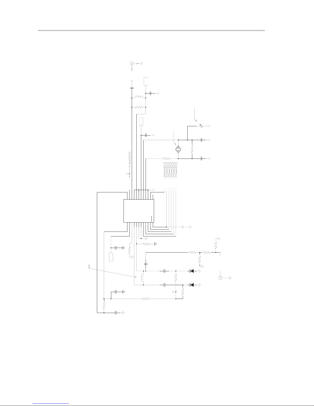
Schematics
2.1 Schematics
J1
TX_OUTTX_OUT
C4
3.3pF
LDET
LOCKDET
20
21
22
23
24
PA_VCC
PA_O UT
PA_G ND
PD_OUT2
LOCKDET
IC1
PD_SET2PLL_VCC
PD_OUT14VCO_TANK15VCO_TANK26PLL_GND7DIG_GND8CLOCK
3
1
R3
19
6.8nHL1LQW1608
51
18
GND
VCC1
C5
16
DIG_VCC
DATA
9
VCC1
C7
0.1uF
15
XOSC117XOSC2
DIG_GND
STROBE11MODE12STDBY
10
0.1uF
13NC14
TRF4900
TXDATA
R4
100
STDBY
MODE
FUNDAMENTAL MODE
CQ1
DATA
STROBE
INITIAL TOLERANCE +/− 7 PPM
CLOCK
STAB OVER TEMP +/− 20 PPM
C10
TEMP RANGE −40TO +85 DEG C
25.6MHz
1000pF
DNP
SELECT FOR OUTPUT
FREQUENCY AT J1
1.5 − 10pF
C13
DNP
SAT
10pF
C12
R7
1.0M
10pF
C11
2-2
NOTES:
DNP: DO NOT PLACE
TBD: TO BE DETERMINED
123
0.1uF
C3
R2
SELECT L2 FOR CENTER FREQUENCY.
SELECT C8, C9 FOR TUNING RANGE.
TYPICAL TUNING RANGE (Vcc=3.3V)
Vt: 0.5 TO 3.0V f: 845−965MHz
SAT: SELECT AT TEST
VCC1
470pF
C2
R1
6.2k
4700pF
C1
100k
R38
100k
C6
DNP
L2
10nH
LQW1608
0
JP1
4.7pF
C9
R5
4.7pF
C8
TP1
TBDR8DNP
R10
SMV1247−079
V2
1
2
10k
1
2
V1
R6
10k
SMV1247−079
TBD
DNP
R9
DNP
TBD
R11
TBD
DNP
VCO_TANK
J2
VCO_TANK
Page 14
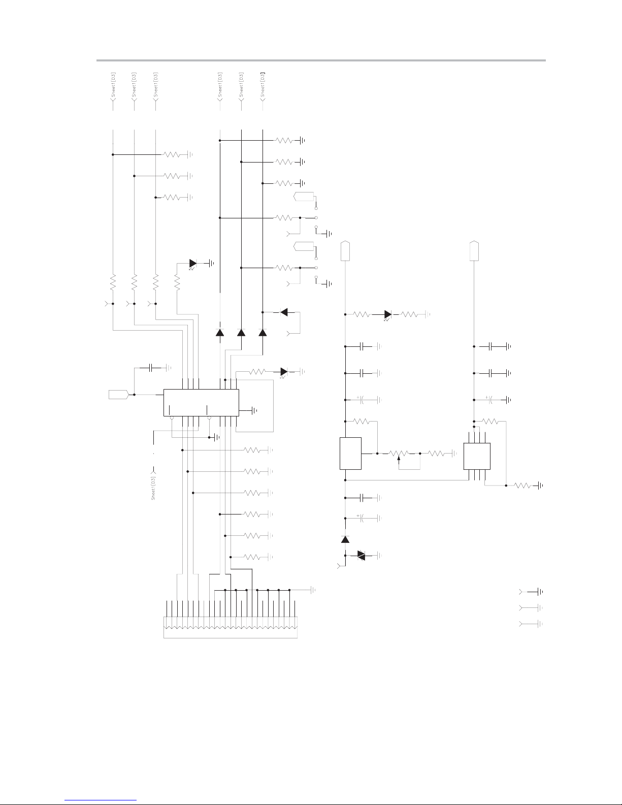
Schematics
MODE
STDBY
CLOCK
DATA
100
R12
DATA
CLOCK
STROBE
10k
R17
10k
R16
10k
R15
LED1
LDET
LN1371SG−(TR)
100
100
R14
R13
STROBE
510
R18
TXDATA
10k
R30
10k
R29
10k
R28
VCC2
100
R27
JP3
2
3 1
MODESTDBYTXDATA
VCC2
100
R26
JP2
2
3 1
LL4148
CR4
VCC1
LN1271R−(TR)
VCC
LED3
220
JP4
0
2.0 − 3.8V (3.0V TYP)
R33
3.3V
VCC2
VCC2
0.1uF
C14
LOCKDET
CR2
LL4148
2Y252Y332Y4
2A2152A3172A4
CR3
LL4148
LL4148
LED2
ENABLE
R25
510
10
SN74LVT244BDW
10k
R24
10k
R23
10k
R22
10k
R21
10k
R20
10k
R19
LN1471SY−(TR)
POWER
13251224112310229218207196185
DB25M
VR1
RED
+8.0V
2
VOUT
VIN
LM317MDT
3
CR5
C19
0.01uF
C18
0.1uF
1.0uF
C17
360
R31
500
1
ADJ
C16
0.1uF
10uF
C15
S1JB
ZR1
SMBJ8.5CA
R32
1
2
220
R34
3
VR2
NC
1VI3VO2VO4
5NC6VO7VO8
ADJ
C22
0.01uF
C21
0.1uF
C20
220
R35
1.0uF
LM317LBD
GROUND CLIPS
R36
360
TP4
TP2 TP3
CR1
9
12
18
20
1Y1161Y2141Y3
IC2
1OE
1A141A261A381A4
1
2
1
P1
7
2Y1
1Y4
2OE112A1
19
13
17416315214
Evaluation Board
2-3
Page 15

Top Side Silkscreen and Drawing
2.1.1 Top Side Silkscreen and Drawing
2-4
Page 16

2.1.2 Bottom Side Silkscreen and Drawing
Top Side Silkscreen and Drawing
Evaluation Board
2-5
Page 17

Parts List
2
7
2
3
2
18 MHz CX−1 SMI
C19 0.01 µF 0603 Ceramic chip capacitor Venkel C0603X7R500−103KNB Venkel C0603X7R500−103KNB
C22 0.01 µF 0603 Ceramic chip capacitor Venkel C0603X7R500−103KNB Venkel C0603X7R500−103KNB
C3 0.1 µF 0603 Ceramic chip capacitor Venkel C0603Y5V160−104ZNB Venkel C0603Y5V160−104ZNB
C5 0.1 µF 0603 Ceramic chip capacitor Venkel C0603Y5V160−104ZNB Venkel C0603Y5V160−104ZNB
C7 0.1 µF 0603 Ceramic chip capacitor Venkel C0603Y5V160−104ZNB Venkel C0603Y5V160−104ZNB
C14 0.1 µF 0603 Ceramic chip capacitor Venkel C0603Y5V160−104ZNB Venkel C0603Y5V160−104ZNB
C16 0.1 µF 0603 Ceramic chip capacitor Venkel C0603Y5V160−104ZNB Venkel C0603Y5V160−104ZNB
C18 0.1 µF 0603 Ceramic chip capacitor Venkel C0603Y5V160−104ZNB Venkel C0603Y5V160−104ZNB
C21 0.1 µF 0603 Ceramic chip capacitor Venkel C0603Y5V160−104ZNB Venkel C0603Y5V160−104ZNB
C17 1 µF 1206 Tantalum Tantalum capacitor
C20 1 µF 1206 Tantalum Tantalum capacitor
C4 3.3 pF 0603 Ceramic chip capacitor Venkel C0603COG500−3R3CNB Venkel C0603COG500−3R3CNB
C8 3.3 pF 0603 Ceramic chip capacitor Venkel C0603COG500−3R3CNB Venkel C0603COG500−3R3CNB
C9 3.3 pF 0603 Ceramic chip capacitor Venkel C0603COG500−3R3CNB Venkel C0603COG500−3R3CNB
C11 10 pF 0603 Ceramic chip capacitor Venkel C0603COG500−100JNB Venkel C0603COG500−100JNB
C12 10 pF 0603 Ceramic chip capacitor Venkel C0603COG500−100JNB Venkel C0603COG500−100JNB
products)
Fast switching diode Diode INC LL4148 Digi-Key LL4148CT−ND
(MINIMELF)
2
Count RefDes Value PatternName Description Manufacturer Part Number Distributor Distributor P/N
2.2 Parts List
2-6
7
Evaluation Board
2
1 C13 1.5 −10 pF 9341 SERIES Trimmer capacitor Johanson 9341−3SL Newark 95F9901
3
2
1 C15 10 µF 6032 C case Tantalum capacitor
1 C6 120 pF 0603 Ceramic chip capacitor Venkel C0603COG500−121JNB Venkel C0603COG500−121JNB
1 C2 470 pF 0603 Ceramic chip capacitor Venkel C0603X7R500−471JNB Venkel C0603X7R500−471JNB
1 C10 1000 pF 0603 Ceramic chip capacitor Venkel C0603X7R500−102KNB Venkel C0603X7R500−102KNB
1 C1 4700 pF 0603 Ceramic chip capacitor Venkel C0603X7R500−472KNB Venkel C0603X7R500−472KNB
1 CQ1 25.6 MHz HC45/U gull wing Resistance weld miniature crystal International Crystal Mfg. 865842
1 CQ1_A1 CX−1−SM Surface-mount quartz crystal CFP − (CMAC frequency
1 CQ1_B1 ATS−SM series Crystal CTS Reeves ATS256SM−T Digi-Key CTX51?TR−ND
4 CR1 MELF3
Page 18

Parts List
2
Fast switching diode Diode INC LL4148 Digi-Key LL4148CT−ND
Fast switching diode Diode INC LL4148 Digi-Key LL4148CT−ND
(MINIMELF)
(MINIMELF)
CR2 MELF3
CR3 MELF3
Fast switching diode Diode INC LL4148 Digi-Key LL4148CT−ND
(MINIMELF)
CR4 MELF3
Texas Instruments SN74LVT244BDW Digi-Key 296−1707−5−ND
Johnson Components 142−0701−801 Newark 90F2624
Johnson Components 142−0701−801 Newark 90F2624
with 3-state outputs
horizontal/PC mount
J1 SMA_H SMA brass connector −
J2 SMA_H SMA brass connector −
horizontal/PC mount
JP2 Jumper−3 pin Breakaway headers AMP 4−103239−0 Newark 90F77252JP3 Jumper−3 pin Breakaway headers AMP 4−103239−0 Newark 90F7725
Panasonic LN1371SG−(TR) Digi-Key P516CT−ND
Panasonic LN1471SY−(TR) Digi-Key P517CT−ND
type-green
type-amber
Panasonic LN1271R−(TR) Digi-Key P490CT−ND
type-red
JP1 0 0603 Chip resistor Venkel CR0603−16W−000B Venkel CR0603−16W−000B
JP4 0 0603 Chip resistor Venkel CR0603−16W−000B Venkel CR0603−16W−000B
4
Count Distributor P/NDistributorPart NumberManufacturerDescriptionPatternNameValueRefDes
1 CR5 SMB Rectifier Diode INC S1JBT Digi-Key S1JBDICT−ND
1 IC1 TSSOP24_M Single chip RF transmitter Texas Instruments TRF4900
1 IC2 SO20WB Octal buffers and line drivers
2
2
1 L1 6.8 nH 0603 Surface-mount inductor Murata LQW1608
1 L2 10 nH 0603 Surface-mount inductor Murata LQW1608
1 LED1 LDET LED, S type Surface-mount LED-Gull wing-S
1 LED2 Enable LED, S type Surface-mount LED-Gull wing-S
1 LED3 VCC LED, S type Surface-mount LED-Gull wing-S
1 P1 DB25M Subminiature D connector AMP 745783−4 Newark 90F5485
2
1 R7 1.0M 0603 Chip resistor Venkel CR0603−16W−105JB Venkel CR0603−16W−105JB
1 R1 6.2k 0603 Chip resistor Venkel CR0603−16W−622JB Venkel CR0603−16W−622JB
Evaluation Board
2-7
Page 19

Parts List
14
6
3
2
R5 10k 0603 Chip resistor Venkel CR0603−16W−103JB Venkel CR0603−16W−103JB
R6 10k 0603 Chip resistor Venkel CR0603−16W−103JB Venkel CR0603−16W−103JB
R15 10k 0603 Chip resistor Venkel CR0603−16W−103JB Venkel CR0603−16W−103JB
R16 10k 0603 Chip resistor Venkel CR0603−16W−103JB Venkel CR0603−16W−103JB
R17 10k 0603 Chip resistor Venkel CR0603−16W−103JB Venkel CR0603−16W−103JB
R19 10k 0603 Chip resistor Venkel CR0603−16W−103JB Venkel CR0603−16W−103JB
R20 10k 0603 Chip resistor Venkel CR0603−16W−103JB Venkel CR0603−16W−103JB
R21 10k 0603 Chip resistor Venkel CR0603−16W−103JB Venkel CR0603−16W−103JB
R22 10k 0603 Chip resistor Venkel CR0603−16W−103JB Venkel CR0603−16W−103JB
R23 10k 0603 Chip resistor Venkel CR0603−16W−103JB Venkel CR0603−16W−103JB
R24 10k 0603 Chip resistor Venkel CR0603−16W−103JB Venkel CR0603−16W−103JB
R28 10k 0603 Chip resistor Venkel CR0603−16W−103JB Venkel CR0603−16W−103JB
R29 10k 0603 Chip resistor Venkel CR0603−16W−103JB Venkel CR0603−16W−103JB
R30 10k 0603 Chip resistor Venkel CR0603−16W−103JB Venkel CR0603−16W−103JB
R4 100 0603 Chip resistor Venkel CR0603−16W−101JB Venkel CR0603−16W−101JB
R12 100 0603 Chip resistor Venkel CR0603−16W−101JB Venkel CR0603−16W−101JB
R13 100 0603 Chip resistor Venkel CR0603−16W−101JB Venkel CR0603−16W−101JB
R14 100 0603 Chip resistor Venkel CR0603−16W−101JB Venkel CR0603−16W−101JB
R26 100 0603 Chip resistor Venkel CR0603−16W−101JB Venkel CR0603−16W−101JB
R27 100 0603 Chip resistor Venkel CR0603−16W−101JB Venkel CR0603−16W−101JB
R33 220 0603 Chip resistor Venkel CR0603−16W−221JB Venkel CR0603−16W−221JB
R34 220 0603 Chip resistor Venkel CR0603−16W−221JB Venkel CR0603−16W−221JB
R35 220 0603 Chip resistor Venkel CR0603−16W−221JB Venkel CR0603−16W−221JB
Panasonic #EVM−1SSX50BXX Digi-Key P1S501CT−ND
potentiometer
R31 360 0603 Chip resistor Venkel CR0603−16W−361JB Venkel CR0603−16W−361JB
R36 360 0603 Chip resistor Venkel CR0603−16W−361JB Venkel CR0603−16W−361JB
R18 510 0603 Chip resistor Venkel CR0603−16W−511JB Venkel CR0603−16W−511JB2R25 510 0603 Chip resistor Venkel CR0603−16W−511JB Venkel CR0603−16W−511JB
14
Count Distributor P/NDistributorPart NumberManufacturerDescriptionPatternNameValueRefDes
2-8
Evaluation Board
1 R3 51 0603 Chip resistor Venkel CR0603−16W−510JB Venkel CR0603−16W−510JB
6
2 R2, R38 100k 0603 Chip resistor Venkel CR0603−16W−104JB Venkel CR0603−16W−104JB
3
2
1 R32 500 P1S Panasonic Surface-mount trimmer
2
Page 20

Parts List
SMV1247−079
SMV1247−079
Electronic
Corp.
Electronic
Corp.
On Semiconductor LM317MDT Newark 06F9320
On Semicondictor LM317LBD Newark 06F9304
70070107373 Digi-Key SJ5303−7−ND
Electronic Specialty
Markets/3M
R8 TBD 0603 Chip resistor Venkel Venkel4R9 TBD 0603 Chip resistor Venkel Venkel
R10 TBD 0603 Chip resistor Venkel Venkel
4
Count Distributor P/NDistributorPart NumberManufacturerDescriptionPatternNameValueRefDes
R11 TBD 0603 Chip resistor Venkel Venkel
2 V1 SC−79 Hyperabrupt tuning varactor Alpha Industries SMV1247−079 Nu Horizons
V2 SC−79 Hyperabrupt tuning varactor Alpha Industries SMV1247−079 Nu Horizons
Three-terminal adustable output
positive voltage regulator
positive voltage regulator
CASE369A−13
CLOCK WHT PC test point Color coded PC test point (white) Components Corp. TP−105−01−09 Newark 97B32538DATA WHT PC test point Color coded PC test point (white) Components Corp. TP−105−01−09 Newark 97B3253
1 VR1 DPAK
1 VR2 SO8NB Three-terminal adustable output
1 ZR1 SMBJ−BI Transient voltage suppressor Vishay/Liteon SMBJ8.5CA Digi-Key SMBJ8.5AGICT−ND
1 8.0V RED PC test point Color coded PC test point (red) Components Corp. TP−105−01−02 Newark 97B3257
8
LDET WHT PC test point Color coded PC test point (white) Components Corp. TP−105−01−09 Newark 97B3253
MODE WHT PC test point Color coded PC test point (white) Components Corp. TP−105−01−09 Newark 97B3253
STDBY WHT PC test point Color coded PC test point (white) Components Corp. TP−105−01−09 Newark 97B3253
STROBE WHT PC test point Color coded PC test point (white) Components Corp. TP−105−01−09 Newark 97B3253
TXDATA WHT PC test point Color coded PC test point (white) Components Corp. TP−105−01−09 Newark 97B3253
TP1 WHT PC test point Color coded PC test point (white) Components Corp. TP−105−01−09 Newark 97B32533TP2 SMD test point Surface-mount test point Components Corp. TP−107−01 Newark 97B26473TP3 SMD test point Surface-mount test point Components Corp. TP−107−01 Newark 97B2647
Evaluation Board
clear
TP4 SMD test point Surface-mount test point Components Corp. TP−107−01 Newark 97B2647
4 FOOT1 Hardware Bumpon hemisphere 0.44 × 20
2-9
Page 21

2.3 EVM DC Voltage Setup
The evaluation board should be used with a dc power supply voltage of 8 V
nominal. Figure 2−1 details the dc voltage supply setup for the TRF4900 EVM.
Figure 2−1.TRF4900 EVM DC Voltage Setup
for LM317 voltage regulator is equal to:
V
out
Vout = 1.25(1+((R32+R34)/R31))
V at terminal 3 of LM317 should be 2 V to 3 V
higher than V
out
V
is equal to 8 V
in
nominal.
With V
V = 7.2 V
GROUND CLIPS
equal to 8 V,
in
POWER
8.0V
RED
TP4TP2 TP3
CR5
S1JB
ZR1
SMBJ8.5CA
C15
10µ F
C16
0.1µ F
R36
360Ω
3
LM317MDT
VIN2VOUT
1
VI
2
VO
3
VO
4
ADJ
LM317LBD
2
VR2
ADJ
1
VR1
3
NC
VO
VO
NC
R32
500Ω
R34
220Ω
2.0 − 3.8 V (3.0 V TYP)
C17 C18
R31
1µ F 0.1µ F 0.01µ F
360Ω
V
Used to Change
adj
V
From 2.2 V to 3.6 V
out
8
7
6
5
R35
C20
220Ω
1µ F 0.1µ F 0.01µ F
C19
C22C21
JP4
0
LED3
VCC
LN1271R−(TR)
R33
220Ω
VCC2
VCC1
3.3V
2-10
Page 22

2.4 Serial Interface and PC Port Pin Out
Figure 2−2 details the serial interface portion of the TRF4900 EVM.
Figure 2−2.TRF4900 EVM Serial Interface
VCC2
P1
DB25M
1
14
2
15
3
16
4
17
5
18
6
19
7
20
8
21
9
22
10
23
11
24
12
25
13
R19
R20
10k
R21
10k
10k
LOCKDET
R23
R22
10k
10k
R24
10k
IC2
1
1OE
2
1A1
4
1A2
6
1A3
8
1A4
19
2OE
11
2A192Y1
13
2A2
15
2A3
17
2A4
10
SN74LVT244BDW
C14
0.1uF
20
18
1Y1
16
1Y2
14
1Y3
12
1Y4
7
2Y2
5
2Y3
3
2Y4
R25
510
LED2
ENABLE
LN1471SY−(TR)
CR1
LL4148
CR2
LL4148
CR3
LL4148
DATA
CLOCK
STROBE
CR4
LL4148
Serial Interface and PC Port Pin Out
R12
100
R13
100
R14
100
R18
510
JP2
2
3 1
LED1
LDET
LN1371SG−(TR)
R26
100
VCC2
MODESTDBYTXDATA
3 1
R27
100
JP3
2
R15
10k
VCC2
R16
R17
10k
10k
R29
R28
10k
10k
R30
10k
DATA
CLOCK
STROBE
MODE
STDBY
TXDATA
P1 Computer Interface Connector Pin Number Function
2 DATA
3 CLOCK
4 STROBE
5 MODE
7 STDBY
9 TXDATA
18 thru 25 Ground
Evaluation Board
2-11
Page 23

Standard PC Parallel Port
2.5 Standard PC Parallel Port
A standard PC parallel port is configured as follows:
113
14 25
Pin
1
2
3
4
5
6
7
8
9
10
11
12
13
14
15
16
17
Note: The TRF4900 EVM uses pins 2–9 for signals from the PC to the EVM.
Description
Strobe
Data 0
Data 1
Data 2
Data 3
Data 4
Data 5
Data 6
Data 7
ACK
Busy
Paper Empty
Select
Auto Feed
Error
Initialize Printer
Select Input
View Is Looking at
Connector Side of
DB-25 Male Connector
PC Output
PC Output
PC Output
PC Output
PC Output
PC Output
PC Output
PC Output
PC Output
PC Input
PC Input
PC Input
PC Input
PC Output
PC Input
PC Output
PC Output
Pin Assignments
Note: 8 Data Outputs
4 Misc Other Outputs
5 Data Inputs
Note: Pins 18−25 Are
Ground
2-12
Page 24

2.6 Jumper Connections
The default position of the jumpers on the TRF4900 EVM are configured as
shown below.
Standard PC Parallel Port
JP1
1
2
JP1 is a 0-Ω 0603 resistor
JP3
1
2
3
JP3 Default is not installed
To R1 and C2 (Loop Filter)
To R5 and R6 (VCO Tank)
To V
CC2
To Mode Test Point
To Ground
2.6.1 Jumper Description
The jumpers on the TRF4900 EVM are used for the following purposes:
- JP1
Jumper JP1 connects the VCO tank circuit to the loop filter of the PLL
circuit. The only reason to remove jumper JP1 is to test the tuning range
of the VCO tank circuit with an external power supply. The default state for
jumper JP1 is JP1-1 to JP1-2. Jumper JP1 is a 0-Ω 0603 resistor.
JP2
1
2
3
JP2 Default is not installed
JP4
1
2
JP4 is a 0-Ω 0603 resistor
To V
CC2
To STDBY Test Point
To Ground
VR1 output (VCC1)
To LED3 anode (Power on LED)
Denotes Default Connection
- JP2
Jumper JP2 can be used to pull the STDBY line up to VCC (JP2-1 to JP2-2)
or pull down to ground (JP2-2 to JP2-3), if a computer connection is not
installed. The primary purpose for JP2 is as a test point to monitor the state
of the STDBY line. The default state for jumper JP2 is not connected.
- JP3
Jumper JP3 can be used to pull the MODE line up to V
(JP3-1 to JP3-2)
CC
or pull down to ground (JP3-2 to JP3-3), if a computer connection is not
installed. The primary purpose for JP3 is as a test point to monitor the state
of the MODE line. The default state for jumper JP3 is not connected.
- JP4
Jumper JP4 connects the Power-On LED to the output of the VR2 voltage
regulator. The default state for jumper JP4 is JP4-1 to JP4-2. Jumper JP4
is a 0-Ω, 0603 resistor.
Evaluation Board
2-13
Page 25

Connectors and Test Points
2.7 Connectors and Test Points
The following information describes the TRF4900 EVM connectors and test
points.
2.7.1 Connectors
- P1
P1 is the PC parallel port interface and is a male DB25 connector. P1 is
connected to the LPT1 or LPT2 port of the computer on which the
TRF4900 software is running.
- J1
TX_OUT is an SMA female connector which is connected to the
transmitter output of the TRF4900.
- J2 VCO_TANK
VCO_T ANK i s a n SMA female connector used with resistors R8, R9, R10,
R11, and capacitor C6 to directly feed in an external VCO signal. Resistors
R8, R9, R10, and R11 are used to form a T attenuator. The components
for this option are not installed on the EVM.
2.7.2 Test Points (TP)
- TP1
- LDET TP
- MODE TP
- STDBY TP
- CLOCK TP
- DATA TP
- STROBE TP
Test point TP1 is used to monitor the tuning voltage applied to the VCO
circuit by the PLL circuit.
The LDET test point is used to monitor the lock detect line of the TRF4900.
The MODE test point is used to monitor the MODE line.
The STDBY test point is used to monitor the STDBY line.
The CLOCK test point is used to monitor the CLOCK signal from the PC.
The DATA test point is used to monitor the DATA signal from the PC.
The STROBE test point is used to monitor the STROBE signal from
the PC.
- TXDATA TP
The TXDATA test point is used to monitor the transmitted data. Transmit
data from an external source can also be applied at this point.
2-14
Page 26

2.7.3 Adjustments
2.7.4 LED Indicators
Connectors and Test Points
Resistor R32 is varied to adjust the VCC1 voltage applied to IC1 (TRF4900).
- VCC LED
If JP4 is installed, the VCC LED is illuminated when voltage is applied to
IC1.
- LDET LED
The LDET LED is illuminated when the lock detect line IC1−23 (TRF4900)
is high, indicating that the PLL circuit is locked.
- ENABLE LED
The ENABLE LED is illuminated when the STDBY line from the computer
is in the high state.
Evaluation Board
2-15
Page 27

2-16
Page 28

Chapter 3
This chapter describes the Windows-based software application that
accompanies the EVM.
Topic Page
3.1 Introduction 3−2. . . . . . . . . . . . . . . . . . . . . . . . . . . . . . . . . . . . . . . . . . . . . . . . . .
3.2 Main Program Screen 3−3. . . . . . . . . . . . . . . . . . . . . . . . . . . . . . . . . . . . . . . . .
3.3 Chip Layout Screen 3−6. . . . . . . . . . . . . . . . . . . . . . . . . . . . . . . . . . . . . . . . . . .
3.4 PLL/Modulation Options Screen 3−7. . . . . . . . . . . . . . . . . . . . . . . . . . . . . . . .
3.5 Testing of Transmitter 3−9. . . . . . . . . . . . . . . . . . . . . . . . . . . . . . . . . . . . . . . . .
Software User’s Guide
3-1
Page 29

Introduction
3.1 Introduction
A Windows-based software application accompanies the evaluation board.
The software is intended for use in either a Windows 95/98 or Windows NT
environment. If the Windows NT environment is used, the Windows NT driver
software must accompany the software. However, if the operating system is
Windows 95/98, the software application can run on its own.
Both the Windows NT Driver and the TRF4900 software are provided on
diskette. Your system administrator must install the Windows NT Driver if you
do not have administrative privileges on your computer. The TRF4900
software can run from the floppy disk by following these steps:
1) Click on the Start button on the desktop
2) Click on the Run button
3) Type − A:\ TRF4900.exe and press OK
3-2
Page 30

3.2 Main Program Screen
Double Click Here With the
n
The screen shown in Figure 3−1 appears on your monitor.
Figure 3−1.Main Program Screen
Main Program Screen
Crystal or Clock
Frequency
Computer Printer Port
LPT1 or LPT2
Transmit Frequency
Press to Program the TRF4900
Left Mouse Button to Obtai
Chip Layout Screen
NOTE: When word bits are displayed in RED, the Send Words Now (F12) button on the main program screen must be pressed
for changes to be updated.
The main program screen is divided into seven main sections as follows:
3.2.1 Synthesizer
This section is used to set the crystal/clock (CLK) frequency, the Desired Freq.,
and the PreScaler value of the divide-by-N of the PLL. From these inputs, the
actual frequency and bit values of Words A and B are calculated.
Software User’s Guide
3-3
Page 31

Main Program Screen
3.2.2 Mode Options
This section allows the user to control various features of the TRF4900. The
following is a brief summary of the four controls.
1) PLL Turns the phase-locked loop on or off.
2) VCO The voltage controlled oscillator (VCO) is always on.
3) Pwr Amp Allows the power amp to be set to off, 20-dB attenuation,
4) LPT Port Allows the user to change between the LPT1 and the
3.2.3 Output Parameters
This section allows the user to turn the TRF4900 Enable, TXData, and Mode
control lines on and off. When the mode control line is off, Mode 0 is defaulted.
When the mode control line is on, Mode 1 is defaulted. Mode 0 initializes using
Words A and D; Mode 1 initializes using Words B and C.
Clock Width and Strobe Width allow the clock and strobe pulse widths to be
increased or decreased.
10-dB attenuation, or 0-dB attenuation states.
LPT2 ports of the controlling computer.
3.2.4 PLL and MM Options
Allows the change of the APLL value (0, 20, 40...140), the NPLL value (256,
512), and the Modulation Mode (FSK).
3.2.5 Help
Gives a brief description of each control box. For example, after clicking the
PLL box in the Mode Options section on the main program screen, the Help
box will read:
Phase-Lock Loop
0: Off
1: On
Valid in Mode 0 or 1.
Most of the other control boxes follow this format. The first line indicates what
portion of the TRF4900 is being controlled. The next two lines indicate the bit
value. If the PLL is off, bit 12 of Words C and D are equal to 0. If it is on, bit 12
is equal to 1. The last line indicates this control works in both Mode 0 and
Mode 1.
Double clicking in the Help box on the main program screen activates the chip
layout screen.
3-4
Page 32

3.2.6 Words
This section updates the binary words after changes are made to the control
options. Clicking on the box next to the word can individually send each word.
Clicking on the Send Words Now (F12) button on the main program screen or
pressing F12 on the keyboard, sends all the words to the TRF4900.
3.2.7 Operation Mode
Operation mode shows whether the TRF4900 is enabled, which mode (0 or
1) is selected, and whether the transmit (TX) data line is on or off.
3.2.8 Changing Values on the Main Program Screen
- Synthesizer Section
CLK Type the desired clock frequency inside the box or use
the arrows located at the right side of the box.
Desired Freq. Type the desired transmit or LO receive frequency inside
the box or use the arrows located at the right side of the
box.
PreScaler Click inside the box to change divide-by-N value
between 256 and 512. The value of NPLL under PLL and
MM Options changes when the PreScaler value
changes.
Main Program Screen
- Mode Options
PLL Click inside the box to turn the PLL on or off (turn on for
transmit).
VCO The VCO is always on. Clicking has no effect.
Pwr Amp Use the arrow at the side of the box to select the desired
power amplifier attenuation.
- Output Parameters
Enable Click inside the box to turn the TRF4900 on or off.
TXData Click inside the box to switch the TXData line between
high and low.
Mode Click inside the box to switch the mode line between 0
and 1.
Clock Width Type inside the box to increase or decrease the clock
pulse width (this should not be changed during normal
use).
Strobe Width Type inside the box to increase or decrease the strobe
pulse width (this should not be changed during normal
use).
Software User’s Guide
3-5
Page 33

Chip Layout Screen
PLL and MM Options
-
APLL: Use the arrows beside the box to select from values of 0,
20, 40, 60, 80, 100, 120, and 140.
NPLL: Click inside the box to change the divide-by-N value
between 256 and 512. The value of PreScaler under
Synthesizer changes when the NPLL value changes.
MM: Modulation Mode is fixed to FSK Modulation Mode.
- LPT Port
LPT_x: Click inside the box to chose between PC parallel ports
LPT 1 or LPT 2.
- Help
Help: When any box on the main program screen is selected
(clicked inside of box with mouse), the Help screen
displays the valid selections for that box. Double clicking
inside the Help box cause the chip layout screen to be
displayed as shown in Figure 3−2.
3.3 Chip Layout Screen
The chip layout screen can be accessed by double clicking on the left mouse
button in the Help section of the main program screen. The chip layout screen
appears as a simplified internal schematic of the TRF4900 as shown in
Figure 3−2.
3-6
Page 34

Figure 3−2.Chip Layout Screen
Press to Turn PLL and VCO On or Off
Mode Select 0 or 1
Enable or Standby.
IC is Disabled in
Standby Mode.
PLL/Modulation Options Screen
Clicking Here Sets
Power Amp
Attenuation (0 dB,
10 dB, 20 dB) or
Turn the Power
Amp Off
Press to Start
FSK Test
Turn TX Data On or Off
Press to Program the TRF4900
- The Mode Options (e.g., the Power Amp, PLL, etc.) may be controlled
from the chip layout screen, as well as from the main program screen.
Changes made in either the main program screen or the chip layout
screen simultaneously update both screens. The user can also control the
chip enable, TXData, and mode control lines from the chip layout screen.
- The user can select FSK Modulation. The FSK T est button, located on the
chip layout screen, will allow the user to transmit data using the TRF4900.
Options for use with the FSK Test button are the pulse repetition frequency
(PRF), which is defaulted to 100 Hz, and the Run Time (Min), which can
be set in minutes. For example, if you want the test to run for five minutes,
set Run Time (Min) to 5.
- The PLL/Modulation Options button brings up the PLL/Modulation
Options screen as shown in Figure 3−3. This button is activated only when
the PLL is on.
3.4 PLL/Modulation Options Screen
Press to Select
PLL/Modulation
Options Screen
The PLL/Modulation Options screen is accessed by pressing the
PLL/Modulation Option button, located on the chip layout screen, and is
displayed as shown in Figure 3−3.
Software User’s Guide
3-7
Page 35

PLL/Modulation Options Screen
Figure 3−3.PLL/Modulation Options Screen
The PLL/Modulations Options screen is divided into the following four
sections:
DV6 Display
Set to 1 by
Double Clicking
f1 Frequency
915 MHz
f
Frequency
2
915.10 MHz
FSK Deviation
of 100 kHz
Send Bits
Button
- APLL
Controls the acceleration factor for the PLL. The values are 0, 20, 40, 60,
80, 100, 120, and 140. Any changes are automatically updated in the PLL
and MM Options section of the main program screen after pressing the
Send Bits button located on the PLL screen.
- NPLL
Controls the N-Divider of the PLL. The NPLL can be set to either 256 or
512. Any changes are automatically updated in the NPLL box on the main
program screen after pressing the Send Bits button located on the PLL
screen.
- Modulation Mode
Allows the user to select FSK modulation. Any changes are automatically
updated in the MM box on the main program screen after pressing the
Send Bits button located on the PLL screen.
- FSK Frequency Register
This section acts as a calculator and sets bits 20−13 of Word D to the user
defined bits. The bits of the FSK deviation register (DV7−DV0) can be set
individually by double clicking inside each DVx box. After setting all bits,
press the Send Bits button located on the PLL/Modulation Options screen.
The bits of the frequency register will be mapped to Word D on the main
program screen, and highlighted in green. Furthermore, Fout: TX_Data
High (MHz), Fout: TX_Data Low (MHz) frequencies, and their difference
(Delta Fout kHz), are calculated and displayed.
Press the Send Bits button located on the PLL/Modulation Options screen to
program the TRF4900. Press the Close button to return to the chip layout
screen.
3-8
Page 36

Testing of Transmitter
3.5 Testing of Transmitter
To test the transmitter section of the TRF4900, perform the following steps:
Step 1: Test Setup:
Set up the test bench as shown in Figure 3−4.
Figure 3−4.Block Diagram for Testing of the TRF4900 EVM Transmitter Section
PC with
TRF4900 software
installed
PC printer port
(LPT1 or LPT2)
Frequency Counter
Spectrum Analyzer
Cable DB25M to DB25F
P1
DB25M
(Male)
TRF4900
Evaluation
Board
Coupled Port
J1
Directional
Coupler
Software User’s Guide
3-9
Page 37

Testing of Transmitter
Step 2: Software Programming:
To test the TRF4900 transmitter section, set the main program screen and the
chip layout screen as shown in Figure 3−5 and Figure 3−6.
Figure 3−5.Main Program Screen
Transmit Frequency
Double Click Here With Left Mouse
Button to Obtain Chip Layout View
3-10
Page 38

Chip Layout Screen of TRF4900 Software for Transmitter Testing
n
ff
Figure 3−6.Chip Layout Screen
Testing of Transmitter
Clicking Here Sets
Power Amp Attenuatio
(0 dB, 10 dB, 20 dB) or
Turn the Power Amp O
Press to Program
TRF4900
After setup is complete, press the Send Words button on the chip layout screen
or the Send Words Now (F12) button on the main program screen to send the
programming words to the TRF4900.
Software User’s Guide
3-11
Page 39

Testing of Transmitter
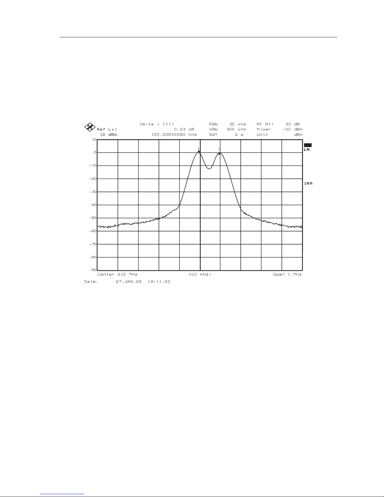
Step 3: Spectrum Analyzer Setup and Clock Offset Procedure
Setup the spectrum analyzer to observe the following:
Figure 3−7.Spectrum Analyzer
Clock Offset Procedure
1) Use the test setup as shown in Figure 3−4 and transmitter software setup
2) Observe the frequency reading on the frequency counter.
3) Subtract 915.000000 MHz from the frequency counter reading.
4) Enter the difference value in the Freq. Error box in the main program
5) Note: If the difference value is negative, enter – sign, followed by the differ-
6) Press the Update CLK button on the main program screen.
7) Verify that clock frequency is updated as shown in Figure 3−9.
8) Pressing the Update CLK button twice clears the frequency offset.
shown in Figure 3−5 and Figure 3−6.
screen as shown in Figure 3−8.
ence value.
Example: Frequency counter reading is 914.996000 MHz
Subtracting 915.000 MHz from 914.996 MHz will yield
a difference of –4000 Hz. This difference is entered in the Freq. Error
block as −0.004 MHz (see Figure 3−8).
3-12
Page 40

Figure 3−8.Input of Frequency Error
Frequency Error is entered here Press Update CLK button
Testing of Transmitter
Figure 3−9.Main Panel Display After Clock Offset Is Applied
Software User’s Guide
3-13
Page 41

Testing of Transmitter
Step 4: FSK Modulation Output Test
On the chip layout screen press the PLL/Modulation Options button.
The PLL/Modulation Options View Is Set Up as Shown in Figure 3−11.
Figure 3−10. Chip Layout View for FSK Modulation Output Test
Select This Button
to Start the FSK
Modulation Test
Select to Program
the TRF4900
Select This Button
With Mouse to Set
FSK Frequency
Set the DVx bits, as shown in Figure 3−11, by double clicking inside each
-
DVx box to set the value to either a 1 or 0. For this example only DV6 is
set to a 1.
- Press the Send Bits button located on the PLL/Modulation Options screen,
to obtain the results shown in Figure 3−11.
- Press the Close button located on the PLL/Modulation Options screen.
3-14
Page 42

Figure 3−11. PLL/Modulation Options Screen
-
Press the Send Words button on the chip layout screen or the Send Words
Now (F12) on the main program screen.
Testing of Transmitter
DV6 Display
Set to 1
f
Frequency
1
915 MHz
f
Frequency
2
915.10 MHz
FSK Deviation
of 100 kHz
Send Bits
Button
- Press the FSK Test button on the chip layout screen, as shown in Figure
3−10, to start the FSK test.
- Set up the spectrum analyzer to observe the spectrum analyzer display
as shown in Figure 3−12.
Software User’s Guide
3-15
Page 43

Testing of Transmitter
.
Figure 3−12. FSK Output From Transmitter
Note: This is FSK modulation with f1 equal to 915.0 MHz, f2 equal to 915.10-MHz and 100-Hz data rate
The f1 frequency is the 0 frequency. The f2 frequency is the 1 frequency.
Figure 3−13. Block Diagram for Testing of the TRF4900 EVM Transmitter Section With an
External Pulse Generator
PC With
TRF4900 Software
Installed
Cable DB25M to DB25F
3 V
Pulse Generator Output Waveform
1 kHz
PC Printer
(LPT1 or LPT2)
P1
DB25M
(Male)
Pulse
Generator
Power
Supply
TRF4900
Evaluation
Board
J1
Spectrum Analyzer
TXDATA TP
GND TP
Coaxial Cable With
Clip Lead Ends
3-16
Page 44
To use an external pulse generator to supply transmit data, set up the test
bench as shown in Figure 3−13.
- Perform the FSK modulation output test as described in the previous
section. In this new setup, an external pulse generator is providing the
modulation. The FSK Test button on the chip layout screen does not need
to be pressed to start the FSK test.
Figure 3−14. FSK Output From Transmitter With an External Modulation
Testing of Transmitter
Note: This is FSK modulation with f1 equal to 915.0 MHz, f2 equal to 915.10-MHz and 1000-Hz data rate.
The f1 frequency is the 0 frequency. The f2 frequency is the 1 frequency.
Software User’s Guide
3-17
Page 45

3-18
 Loading...