

Page 1

User's Guide
SLWU076A–November 2011–Revised July 2012
TRF3765 Integer/Fractional-N PLL With Integrated VCO
Evaluation Module
This document describes usage and features of the TRF3765 evaluation module (EVM) for wideband
frequency synthesis applications. The synthesizer uses an integer/fractional-N PLL with integrated VCOs
to generate local oscillator signals from 300 MHz to 4800 MHz. This document describes rapid-start setup
procedures, detailed descriptions of circuit blocks and available options, schematics and printed-circuit
board layout, and a common start-up problem troubleshooting guide.
Contents
1 Quick-Start Operating Procedures ........................................................................................ 2
2 Circuit Block Descriptions .................................................................................................. 2
2.1 Test Points .......................................................................................................... 2
2.2 Power Supply ....................................................................................................... 3
2.3 Loop Filter ........................................................................................................... 3
2.4 SPI Communication ................................................................................................ 4
2.5 Reference Clock ................................................................................................... 4
3 Configuration Options ...................................................................................................... 4
4 Physical Description ........................................................................................................ 5
4.1 Schematic ........................................................................................................... 5
4.2 Layout ............................................................................................................... 8
4.3 Bill of Materials .................................................................................................... 12
5 Troubleshooting FAQs .................................................................................................... 15
List of Figures
1 Loop Filter Reference Designators ....................................................................................... 4
2 TRF3765EVM Schematic, Page 1 of 3 .................................................................................. 5
3 TRF3765EVM Schematic, Page 2 of 3 .................................................................................. 6
4 TRF3765EVM Schematic, Page 3 of 3 .................................................................................. 7
5 Silkscreen, Top.............................................................................................................. 8
6 Top Layer and Drill Map ................................................................................................... 9
7 Layer 2, Ground ........................................................................................................... 10
8 Layer 3, Power............................................................................................................. 11
9 Bottom Layer and Silkscreen ............................................................................................ 12
10 Fabrication Drawing....................................................................................................... 12
List of Tables
1 Test Point Color Codes .................................................................................................... 2
2 Integer and Fractional Mode Configurations ............................................................................ 5
3 Fractional Board Bill of Materials........................................................................................ 12
4 Integer Board Bill of Materials, Differences from Fractional Board ................................................. 14
5 Troubleshooting Sequences ............................................................................................. 15
SLWU076A–November 2011–Revised July 2012 TRF3765 Integer/Fractional-N PLL With Integrated VCO Evaluation Module
Submit Documentation Feedback
Copyright © 2011–2012, Texas Instruments Incorporated
1
Page 2
Quick-Start Operating Procedures
1 Quick-Start Operating Procedures
The TRF3765 evaluation module (EVM) is preconfigured to use a 3.3-Vdc power supply on TP2. The
supply must be capable of supplying 250 mA.
SPI communication is required for configuring the TRF3765 device. J7 accepts a mini-USB connector that
can be driven through the device graphical user interface (GUI).
Local oscillator (LO) outputs are available in four differential pairs on SMA coaxial connectors J1, J3-J6,
and J9-J11.
The following steps describe the EVM setup for basic operation with the default hardware configuration.
1. Connect the mini-USB connector. LED D1 draws power through the mini-USB connector and
illuminates immediately.
2. Power the device by supplying TP2 with 3.3 V. Use TP3 for the ground connection. Board revisions
prior to Revision D may require additional power supply connections.
3. Connect the LO output to measurement equipment.
4. Install and start the GUI software.
5. Initiate a communication link with the device by using the GUI Connect button. Follow on-screen
instructions to load a register configuration file. Select file TRF3765.FracMode.3p3Vtank.2600MHz.txt
for a fractional mode board and TRF3765.IntMode.3p3Vtank.2600MHz.txt for an integer mode board.
6. Verify lock-detect on LED D2 and the signal on measurement equipment. If D2 is not illuminated, no
signal is present or the signal is at the incorrect frequency. Check GUI settings on any of the High
Level tabs and recalibrate.
7. Using default hardware and configuration settings, fractional mode integrate phase noise is –47 dBc to
–48 dBc/Hz, whereas integer mode integrated phase is –44 dBc/Hz.
www.ti.com
2 Circuit Block Descriptions
This section describes each of the major circuit blocks and their configuration options.
2.1 Test Points
Test points are used throughout the board for control and monitoring. These test points are color-coded
for quick reference. The color codes are described in Table 1.
Color Group Reference Designators
Black Ground TP1, TP3, TP4, TP11, TP14, TP27-TP30
White Unregulated supply TP2, TP24
Red Unregulated supply TP5
Purple Regulated supply TP25, TP26
Green VCC and SPI monitor TP6-TP10, TP12, TP13, TP19-TP23
Blue VCC1 monitor TP15-TP18
Table 1. Test Point Color Codes
2
TRF3765 Integer/Fractional-N PLL With Integrated VCO Evaluation Module SLWU076A–November 2011–Revised July 2012
Copyright © 2011–2012, Texas Instruments Incorporated
Submit Documentation Feedback
Page 3

www.ti.com
2.2 Power Supply
The TRF3765 uses three primary power supplies: VCC1, VCC2, and VCC3. In the default configuration,
VCC1 and VCC2 are connected onboard by R41 and VCC3 is unused. The entire board can be supplied
through 3.3 V on TP2 or Revision D boards. Earlier board revisions require multiple power connections.
A clean power supply is critical to optimal phase noise performance of the synthesizer. The impact of the
power supply is discussed in detail in the application report Supply Noise Effect on Oscillator Phase Noise
(SLWA066). Linear power supplies are the best sources available. Switching power supplies degrade inband phase noise by 10 dB compared to linear laboratory supplies. Onboard regulators U3 and U4 are
ultra-clean TPS74201 linear regulators that also provide excellent performance when they are driven by
most laboratory power supply equipment. These regulators provide performance comparable to a clean
linear supply. To use these regulated 3.3-V supplies, disconnect power from TP2 and remove R41.
Connect 5 V to TP26, using TP27 for ground. Place jumpers on JP4 and JP5 to shunt jumper pins 1 and
2.
VCC3 can be used to drive VCC_TK, a 3.3-V/5-V tolerant supply on the TRF3765. VCC_TK is normally
driven by the 3.3-V VCC2 supply, but some applications perform better with a 5-V supply on VCC_TK. To
use VCC3 to drive VCC_TK at 5 V, move FB2 onto FB11. Populate R12 with a short. Then drive VCC3
through TP5 with a clean linear laboratory supply at 5 V.
VCC3 can also be driven at 5 V by onboard regulator U5. However, this regulator is not as clean as a
linear laboratory supply, and some phase noise performance loss occurs. To use the VCC3 onboard 5-V
regulator, drive TP25 with 6 V using TP28 for ground and place a jumper on JP1 to shunt jumper pins 1
and 2.
The TRF3765EVM includes a power supply filter. This filter can be used to reduce in-band frequency
noise from a switching power supply so that an external supply can drive 5 V on VCC_TK. Phase noise
performance using a high-quality laboratory switching power supply to drive VCC3 through TP5 is similar
to performance measured using a linear supply. The filter is integrated on Rev. E and later boards. Rev. D
and earlier boards include an external filter that is equipped with BNC connectors for a convenient
connection with power supply banana jacks.
Each VCC pin on the TRF3765 connects to an individual test point. The test point may be used for
monitoring. Because each supply pin is isolated through a ferrite bead, by lifting the ferrite bead these test
points may also be used to drive single-device supply pins.
Spurs occurring in the LO signal at 60 kHz and 100 kHz offset from the carrier are usually the result of
ground loops in power supply cabling.
Circuit Block Descriptions
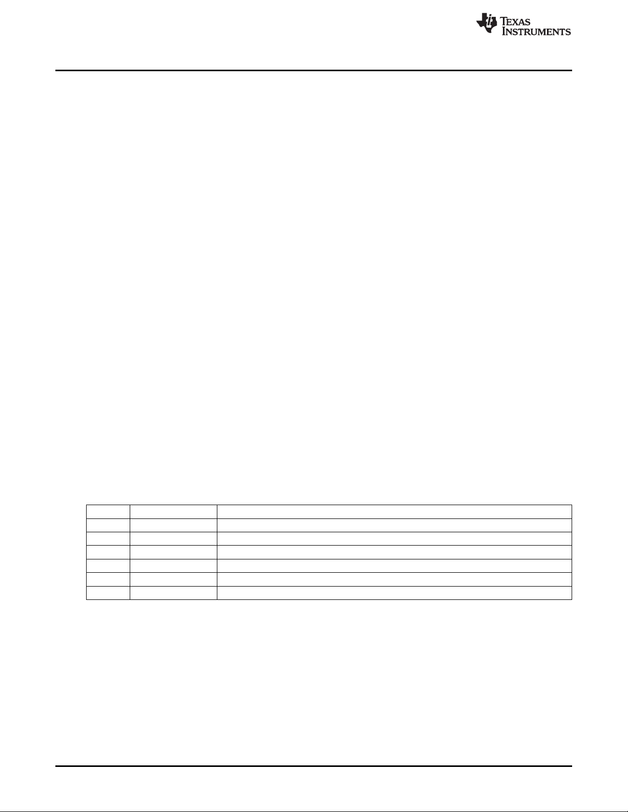
2.3 Loop Filter
Loop-filter components are also critical to optimal phase noise performance. The loop filter must be
matched to the selected phase frequency detector (PFD) frequency. TRF3765 boards are shipped with
components matched to the onboard reference clock and configuration file. However, to use a different
PFD frequency, the loop-filter components must be updated. The Loop Filter Design Tool available at
ti.com in the TRF3765EVM product folder is an intuitive software package that identifies proper
component values.
Loop filter reference designators are shown in Figure 1. The assembly layout of these components is
shown in a silkscreen blow-up on the EVM.
SLWU076A–November 2011–Revised July 2012 TRF3765 Integer/Fractional-N PLL With Integrated VCO Evaluation Module
Submit Documentation Feedback
Copyright © 2011–2012, Texas Instruments Incorporated
3
Page 4
R5
R6
C1 C2 C3
R4
C4
CP_OUT
VTUNE_IN
CP_REF
VTUNE_REF
R15R13
R20
R45
R46
TP12
VCC2
Configuration Options
VTune may be monitored on TP12 without disrupting circuit operation, because R20 is a high-value
resistance. TP12 can also be used to drive VTune for open-loop VCO measurements when the TRF3765
charge pump is in 3-state logic. A 1-µF capacitor on C4 is also recommended for open-loop
measurements to help stabilize the applied voltage.
By default, reference is tied to ground through shorts on R13, R15, and R45, with R46 open.
www.ti.com
Figure 1. Loop Filter Reference Designators
2.4 SPI Communication
SPI communication from the TRF3765 GUI passes through mini-USB connector J7. The USB interface is
decoded and encoded by U2 into SPI lines DATA, STROBE, CLK, and RDBK. U2 is powered through the
USB connection instead of the board supply, and LED D1 indicates USB power is applied. Test points
TP6–TP10 can be used to monitor SPI communication with laboratory equipment. The laboratory
equipment must be set to high impedance so that it does not load the communication lines.
When the USB cable is disconnected, U2 I/Os are high impedance. In this case, TP6–TP10 can be used
to directly drive the SPI lines.
The power-on reset default register settings in the TRF3765 do not correspond to a valid operational state.
SPI initialization is required to operate the device. Once the registers have been initialized, the mini-USB
cable may be disconnected without disrupting device operation. However, once the mini-USB has been
reconnected, the link must be reestablished through the GUI Connect button on the Start Up tab. The link
exists between the GUI computer and U2, so loss of power to the TRF3765 device does not require
reestablishing the link. Loss of device power, however, does require re-initialization of the registers.
2.5 Reference Clock
An oscillator is installed on the TRF3765EVM to provide a reference clock to the device. JP2 installed
provides supply voltage to the oscillator, whereas JP3 installed connects the oscillator output to the
TRF3765. The oscillator frequency drifts over temperature and is not rated for the full TRF3765
temperature operating range, so temperature testing must use an external reference clock.
An external reference clock can be supplied through the SMA connector J8. When using an external
reference clock, remove jumpers on JP2 and JP3. The external reference is ac-coupled to the TRF3765
input pin. An external reference can also be used to frequency-lock the device to laboratory equipment.
Verify that any supplied reference clock has low phase noise.
3 Configuration Options
The TRF3765 evaluation module ships configured for either integer mode or fractional mode. Each
configuration is designed to use different reference and PFD frequencies and also has the corresponding
loop-filter components. Differences in integer mode and fractional mode boards are listed in Table 2.
4
TRF3765 Integer/Fractional-N PLL With Integrated VCO Evaluation Module SLWU076A–November 2011–Revised July 2012
Copyright © 2011–2012, Texas Instruments Incorporated
Submit Documentation Feedback
Page 5
C41
47pF
C17
47pF
DNI
D2
LD
LED AMBER
12
C23
1uF
C72
0.1uF
DNI
C31
47pF
C53
1uF
C3
10nF
R10
0
DNI
1K
FB2
C21
10nF
R23 100
J4
LO4_OUTP
1
5234
SMA
END
TP18
BLU
VCC_LO4
C51
4.7pF
C28
1uF
1K
FB11
DNI
1K
FB4
C38
47pF
C59
10nF
R3 0
J5
LO1_OUTP
1
5234
SMA
END
R34
0
DNI
TP20
GRN
VCC_DIG
1K
FB13
C37
1uF
R19
15K
TP15
BLU
VCC_LO1
J9
LO3_OUTM
1
5234
SMA
END
C18
10nF
R40
0
DNI
R24 100
C8
4.7pF
R12
0
DNI
C49
27pF
C11
47pF
C12
10nF
R7 0
TP13
GRN
VCC_TK
U1
TRF3765
GND_DIG
1
VCC_DIG
2
DATA
3
CLOCK
4
STROBE
5
READBACK
6
VCC_DIV
7
GND_BUFF1
8
LO1_OUTP9LO1_OUTM10LO2_OUTM11LO2_OUTP12LO3_OUTP13LO3_OUTM14LO4_OUTM15LO4_OUTP
16
GND_BUFF2
17
EXTVCO_IN
18
EXTVCO_CTRL
19
VCC_TK
20
VCC_OSC
21
GND_OSC
22
VTUNE_IN
23
VTUNE_REF
24
CP_REF25CP_OUT26VCC_CP
27
VCC_PLL
28
GND
29
REF_IN
30
GND
31
LD
32
PWRPAD
33
R27 100
1K
FB12
C50
1uF
1K
FB6
R30
0
DNI
R11 0
C9
1uF
J11
LO2_OUTM
1
5234
SMA
END
R25 100
C10 4.7pF
R28 100
J1
LO1_OUTM
1
5234
SMA
END
C52
10nF
C39
1uF
1K
FB5
C6
47pF
C7
27pF
R33 0
1K
FB15
R37
0
DNI
C27
27pF
TP8
GRN
LD
TP23
GRN
VCC_OSC
C13
10nF
R26 100
TP19
GRN
VCC_DIV
C43
.1uF
DNI
C47
47pF
C54
1uF
J2
EXT_VCO
1
5234
SMA
END
TP22
GRN
VCC_CP
R29 0
R35 0
SJP1
EXTVCO_CTRL_OUT
1
3
2
C55
27pF
J3
LO4_OUTM
1
5234
SMA
END
C56
10nF
C45
1uF
C57
4.7pF
C44
47pF
DNI
TP16
BLU
VCC_LO2
R39
0
DNI
R31 0
R1
49.9
DNI
C46
47pF
J6
LO3_OUTP
1
5234
SMA
END
TP21
GRN
VCC_PLL
C16
.1uF
DNI
C48
27pF
R22 100
TP17
BLU
VCC_LO3
R36
0
DNI
1K
FB8
1K
FB14
J10
LO2_OUTP
1
5234
SMA
END
C22
4.7pF
C32
47pF
C40
1uF
R21 100
1K
FB1
R32
0
DNI
C24
4.7pF
R2 0
LO1P
LO1M
LO2M
LO2P
LO3P
LO3M
LO4M
LO4P
EXTVCO
EXT_VCO
LO1_P
LO1_M
LO2_M
LO2_P LO3_P
LO3_M
LO4_M
LO4_P
GNDGND GND
GND
GND
GND
GND
GNDGND GND GND
GND
GND
GND
GNDGND GND
GND
GND
GND
GND
GNDGND GND GND
GND
GND
GND GND
VCC2
GND GNDGND
VCC2
GND
GND GND
GND
VCC2
GND
GND
GND GND
VCC1
GND
VCC3
VCC2
GNDGND
GND
GND GND GND
VCC2
GND GND
GND
GND
VCC2
GND
GND
VCC1
VCC1
VCC1
VCC1
GND
GND
DATASH2
CLKSH2
STROBESH2
RDBKSH2
REFINSH2
RF_VTUNE SH2
RF_CP_OUT SH2
RF_CP_REF
RF_VTUNE_REF
SHUNT 2-3
www.ti.com
Item Fractional Mode Integer Mode
Oscillator Y1 frequency 61.44 MHz Y1 frequency 40 MHz
Typical PFD frequency 30.72 MHz 1.6 MHz
Loop filter components R5 = 475 Ω R5 = 5 kΩ
Configuration file TRF3765.FracMode.3p3Vtank.2600MHz.txt TRF3765.IntMode.3p3Vtank.2600MHz.txt
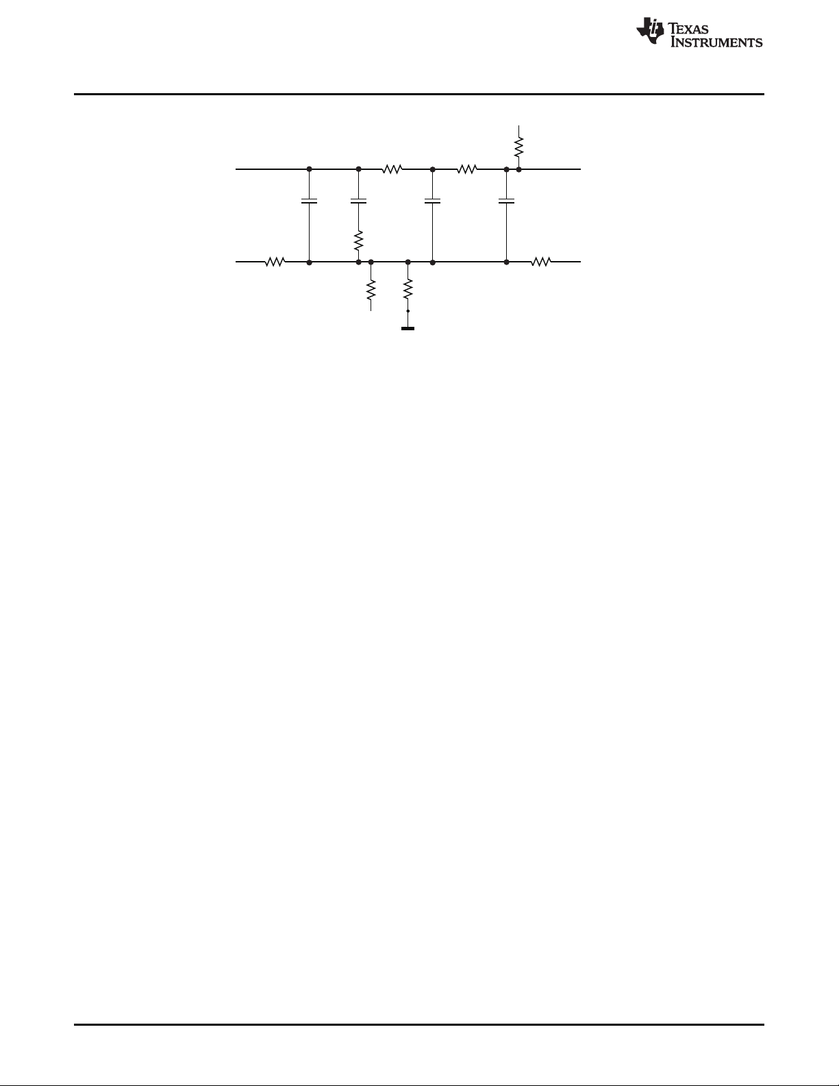
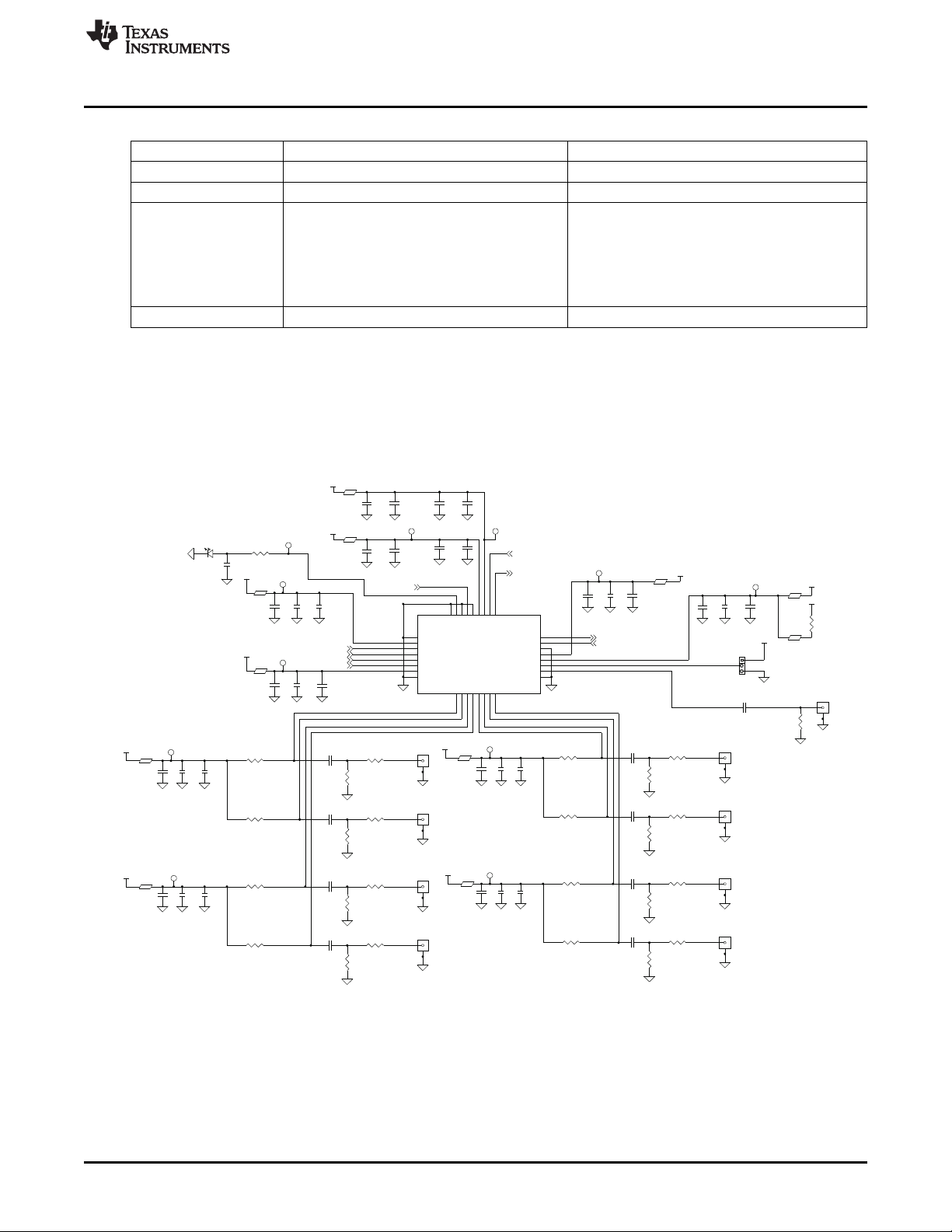
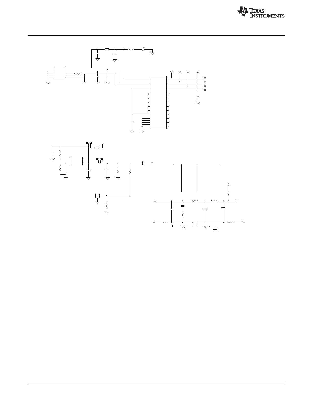
4 Physical Description
The TRF3765EVM is designed to be a high-performance platform for the TRF3765 device. This section
describes the schematic, layout and stackup, and bill of materials corresponding to Revision D boards.
4.1 Schematic
Physical Description
Table 2. Integer and Fractional Mode Configurations
C20 = 2200 pF C20 = 47 pF
C19 = 22000 pF C19 = 560 pF
R6 = 475 Ω R6 = 10 kΩ
C14 = 220 pF C14 = 4.7 pF
R4 = 475 Ω R4 = 0 Ω
C15 = 220 pF C15 = open
SLWU076A–November 2011–Revised July 2012 TRF3765 Integer/Fractional-N PLL With Integrated VCO Evaluation Module
Submit Documentation Feedback
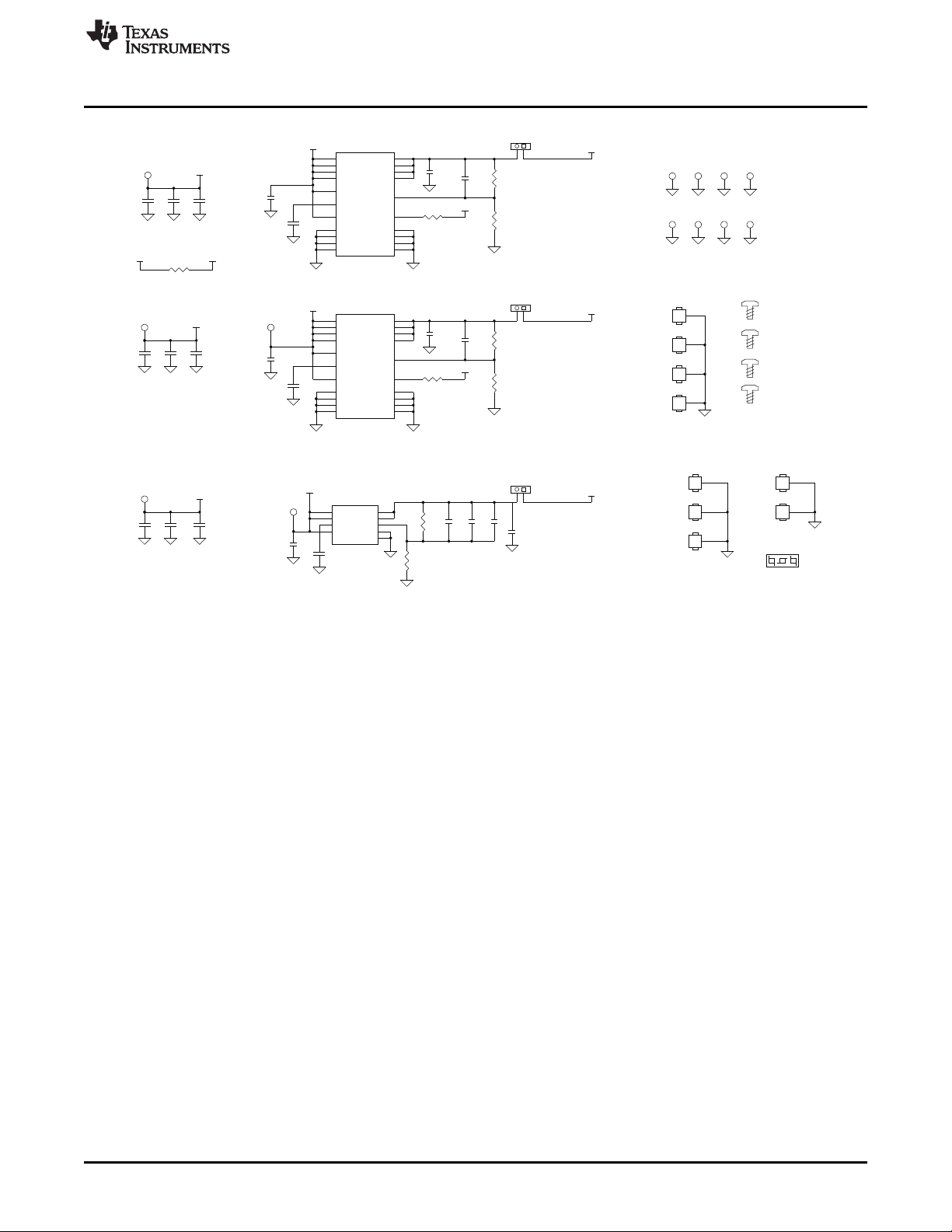
Figure 2. TRF3765EVM Schematic, Page 1 of 3
Copyright © 2011–2012, Texas Instruments Incorporated
5
Page 6
TP6
GRN
RDBK
C34
.1uF
1K
FB10
C19
560pF
1 2
R17
1K
12
R8
15K
R14
10K
DNI
12
C67
100pF
J8
EXT_REF
1
5234
SMA
END
R15
0
1 2
R6
10K
12
R18
0
DNI
1 2
R5
4.99K
1 2
JP3
1
2
C30
.1uF
DNI
1 2
C35
47pF
R16
49.9
DNI
1 2
R45 0
R4
0
1 2
D1
USB_PWR
LED AMBER
1 2
120
FB7
J7
USB_SUPER-MINI_AB
VBUS
1
D-
2
D+
3
ID
4
GND
5
GND1
6
GND2
7
GND3
8
GND4
9
C26 22pF
C36
.1uF
C25
.01uF
TP10
GRN
DATA
R20
1M
12
C14
4.7pF
1 2
Y1
TSM75-1148-40.000M
EN1VCC
4
OUT3GND
2
C29
47pF
C15
2.2pF
DNI
1 2
TP9
GRN
CLK
U2
FT245RL
USBDM
16
USBDP
15
VCCIO
4
NC1
8
RESET
19
NC2
24
OSCI
27
OSCO
28
3V3OUT
17
AGND
25
GND
7
GND
18
GND
21
TEST26PWREN
12
WR
14
D1
5
D7
6
D5
9
D6
10
TXE
22
D4
2
D3
11
RXF
23
D0
1
RD
13
VCC
20
D2
3
C20
47pF
1 2
TP7
GRN
STROBE
C33
.1uF
1 2
TP11
BLK
GND
R9
0
12
JP2
1
2
R13
0
1 2
R38 0
R46 0
DNI
TP12
GRN
VTUNE
EXT_REF
GND
GND
GND GNDGND GND
GND GND
GND GND
GND
GND
GND
GNDGND
GND
VCC2
GND
GND
VCC2
RF_CP_OUTSH1
RF_VTUNE SH1
REFIN SH 1
CLK SH1
DATA SH1
RDBK SH1
STROBE SH1
RF_VTUNE_REF SH1RF_CP_REFSH1
SERIAL INTERFACE
RF/IF FREQ REF
INTERFACE
TABLE 1
INTEGER FRACTIONAL
C14
C15
C19
C20
R4
R5
R6
4.7pF
DNI
560pF
47pF
0
4.99K
10K
220pF
220pF
22000pF
2200pF
470pF
470pF
470pF
Physical Description
www.ti.com
6
TRF3765 Integer/Fractional-N PLL With Integrated VCO Evaluation Module SLWU076A–November 2011–Revised July 2012
Figure 3. TRF3765EVM Schematic, Page 2 of 3
Copyright © 2011–2012, Texas Instruments Incorporated
Submit Documentation Feedback
Page 7
TP4
BLK
GND
SCREW PHIL 4-40 X 3/8"
C5
1uF
SH5
RF SHIELD
1
TP2
WHT
VCC1_+3.3V
MT1
1
C65
1uF
U3
TPS74201RGW
IN15OUT1
1
BIAS
10
SS
15
EN
11
OUT2
18
OUT3
19
OUT4
20
IN2
6
IN3
7
IN4
8
FB/SNS
16
PG
9
NC1
2
NC2
3
NC3
4
NC4
13
NC5
14
NC6
17
GND
12
PAD
21
MT2
1
TP1
BLK
GND
JP1
VCC3_+5V
1
2
C63
10uF
TP5
RED
VCC3_+5V
TP27
BLK
GND
C58
100uF
MT3
1
R48 10K
SH1
RF SHIELD
1
TP25
PURPLE
+6.0V
TP26
PURPLE
+5.0V
C1
.1uF
MT4
1
TP29
BLK
GND
C79
10uF
C66
.1uF
R49
52.3K
SH2
RF SHIELD
1
C64
1uF
TP28
BLK
GND
C80
10uF
C74
160pF
TP30
BLK
GND
C69
100uF
SH3
RF SHIELD
1
BARE BOARD, TRF3765
C2
1uF
C81
10uF
C68
1uF
JP4
VCC2_+3.3V
1
2
C75
10uF
SH4
RF SHIELD
1
C70
10uF
TP24
WHT
VCC2_+3.3V
C42
100uF
C76
10uF
U5
TPS7A8001
OUT1
1
OUT2
2
GND
4
NR
6
EN
5
IN2
7
FB/SNS
3
IN1
8
PAD
9
TP14
BLK
GND
U4
TPS74201RGW
IN15OUT1
1
BIAS
10
SS
15
EN
11
OUT2
18
OUT3
19
OUT4
20
IN2
6
IN3
7
IN4
8
FB/SNS
16
PG
9
NC1
2
NC2
3
NC3
4
NC4
13
NC5
14
NC6
17
GND
12
PAD
21
R50
31.6K
R52
31.6K
R47
10K
C4
.1uF
TP3
BLK
GND
R51
10.2K
SCREW PHIL 4-40 X 3/8"
R53
10.2K
SCREW PHIL 4-40 X 3/8"
C73
10uF
C62
1uF
R54 10K
JP5
VCC1_+3.3V
1
2
C78
10uF
SCREW PHIL 4-40 X 3/8"
GND
GND
GND
GND
GND
GNDGND GND
VCC2
GND
GND
GND
GND GND
VCC1
VCC3
GNDGND
GND GND
+6.0V
VCC3
GND
+5.0V
GND
+5.0V
GND
VCC2
GND
+5.0V
GND
+5.0V
GND
VCC1
GND
GND
GND
GND
GND
GND
GND
GND
GND
GND
GND
GND
GND
RF FENCE AND COVER
QTY 1
BOARD HARDWARE
NO SHUNT
NO SHUNT
NO SHUNT
R48 0
VCC2
VCC1
C82
4.7uF
GND
www.ti.com
Physical Description
Figure 4. TRF3765EVM Schematic, Page 3 of 3
Copyright © 2011–2012, Texas Instruments Incorporated
SLWU076A–November 2011–Revised July 2012 TRF3765 Integer/Fractional-N PLL With Integrated VCO Evaluation Module
Submit Documentation Feedback
7
Page 8

Physical Description
4.2 Layout
www.ti.com
Figure 5. Silkscreen, Top
8
TRF3765 Integer/Fractional-N PLL With Integrated VCO Evaluation Module SLWU076A–November 2011–Revised July 2012
Copyright © 2011–2012, Texas Instruments Incorporated
Submit Documentation Feedback
Page 9

www.ti.com
Physical Description
Figure 6. Top Layer and Drill Map
SLWU076A–November 2011–Revised July 2012 TRF3765 Integer/Fractional-N PLL With Integrated VCO Evaluation Module
Submit Documentation Feedback
Copyright © 2011–2012, Texas Instruments Incorporated
9
Page 10

Physical Description
www.ti.com
Figure 7. Layer 2, Ground
10
TRF3765 Integer/Fractional-N PLL With Integrated VCO Evaluation Module SLWU076A–November 2011–Revised July 2012
Copyright © 2011–2012, Texas Instruments Incorporated
Submit Documentation Feedback
Page 11

www.ti.com
Physical Description
Figure 8. Layer 3, Power
SLWU076A–November 2011–Revised July 2012 TRF3765 Integer/Fractional-N PLL With Integrated VCO Evaluation Module
Submit Documentation Feedback
Copyright © 2011–2012, Texas Instruments Incorporated
11
Page 12

Physical Description
www.ti.com
Figure 9. Bottom Layer and Silkscreen
Figure 10. Fabrication Drawing
4.3 Bill of Materials
Table 3. Fractional Board Bill of Materials
Item
Qty Note Part Reference Value PCB Footprint Manufacturer Manufacturer Part No.
No.
1 6 C1, C4, C33, C34, C36, 0.1uF 0402 PANASONIC ECJ-0EB1C104K
2 13 C2, C5, C9, C23, C28, 1uF 0402 PANASONIC ECJ-0EB1A105M
3 8 C3, C12, C13, C18, C21, 10nF 0402 MURATA GRM155R71E103KA01D
4 8 C6, C11, C31, C32, C38, 47pF 0402 AVXCORP GRM1555C1H470JZ01
5 5 C7, C27, C48, C49, C55 27pF 0402 AVX 04025A270JAT2A
6 6 C8, C10, C22, C24, C51, 4.7pF 0402 MURATA GRM1555C1H4R7CZ01D
7 2 C14, C15 220pF 0402 AVX 04023A221JAT2A
8 1 C82 4.7uF 0805 TDK CORP C2012X5R1A475K/0.86
9 0 DNI C16, C30, C43 0.1uF 0402 PANASONIC ECJ-0EB1A104K_DNI
10 0 DNI C17, C44 47pF 0603 MURATA GRM1885C1H470JA01D_DNI
C66
C37, C39, C40, C45, C50,
C53, C54, C68
C52, C56, C59
C41, C46, C47
C57
12
TRF3765 Integer/Fractional-N PLL With Integrated VCO Evaluation Module SLWU076A–November 2011–Revised July 2012
Copyright © 2011–2012, Texas Instruments Incorporated
Submit Documentation Feedback
Page 13

www.ti.com
Physical Description
Table 3. Fractional Board Bill of Materials (continued)
Item
Qty Note Part Reference Value PCB Footprint Manufacturer Manufacturer Part No.
No.
11 1 C19 22000pF 0402 MURATA GRM155R71C223KA01D
12 1 C20 2200pF 0402 AVX 04025C222JAT2A
13 2 C29, C35 47pF 0402 PANASONIC ECJ-0EC1H470J
14 1 C25 0.01uF 0402 PANASONIC ECJ-0EB1E103K
15 1 C26 22pF 0402 PANASONIC ECJ-0EC1H220J
16 3 C42, C58, C69 100uF 1210 PANASONIC ECJ-4YB0J107M
17 3 C62, C64, C65, 1uF 0805 TDK CORP C2012X5R1E105K
18 9 C63, C70, C73, C75, C76, 10uF 0603 MURATA GRM188R60J106ME47D
19 1 C67 100pF 0402 MURATA GRM1555C1H101JZ01D
20 0 DNI C72 0.1uF 0402 PANASONIC ECJ-0EB1A104K_DNI
21 1 C74 160pF 0603 TDK Corp C1608C0G1H161J
22 2 D1, D2 LED AMBER LED_0805 PANASONIC LNJ406K54RX
23 11 FB1,FB2, FB4-FB6, FB8, 1K IND_0402 MURATA BLM15AG102SN1
24 1 FB7 120 IND_0402 MURATA BLM15AG121SNIB
25 0 DNI FB11 1K IND_0402 MURATA BLM15AG102SN1_DNI
26 10 J1-J6,J8-J11 SMA_END_JACK SMA_SMEL_250x215 Johnson 142-0711-821
7 1 J7 USB_SUPER-MINI_AB CON_SMRT_USBMNE20_F ACON MNE20-5G5P10
28 5 JP1-JP5 JUMPER_1X2_100 HDR_THVT_1X2_100_M SAMTEC TSW-102-07-L-S
29 4 MT1-MT4 STANDOFF4-40 X 0.500" mfg125_plated KEYSTONE 3480
30 0 DNI R1 R16 49.9 0402 PANASONIC ERJ-2RKF49R9X_DNI
31 12 R2,R3, R7, R9, R11, R13, 0 0402 PANASONIC ERJ-2GE0R00X
32 3 R4, R5, R6 470 0402 PANASONIC ERJ-2RKF4700X
33 2 R8, R19 15K 0402 PANASONIC ERJ-2GEJ153X
34 0 DNI R10, R12, R18, R30, R32, 0 0402 PANASONIC ERJ-2GE0R00X_DNI
35 0 DNI R14 10K 0402 PANASONIC ERJ-2GEJ103X_DNI
36 1 R17 1K 0402 PANASONIC ERJ-2GEJ102X
37 1 R20 1M 0402 PANASONIC ERJ-2RKF1004X
38 8 R21, R22-R28 100 0402 PANASONIC ERJ-2RKF1000X
39 2 R38, R41 0 0603 Panasonic ERJ-3GEY0R00V
40 3 R47, R48, R54 10K 0603 PANASONIC ERJ-3EKF1002V
41 1 R49 52.3K 0603 PANASONIC ERJ-3EKF5232V
42 2 R50, R52 31.6K 0603 PANASONIC ERJ-3EKF3162V
43 2 R51, R53 10.2K 0603 PANASONIC ERJ-3EKF1022V
44 0 DNI SH1-SH5 RF SHIELD MFG053_PTH LEADER TECH SL-10797
45 0 DNI SJP1 SOLDER JUMPER, 0603 SJP3_JUMPER DNI DNI
46 8 TP1, TP4, TP11, TP14, BLK TP_THVT_100_RND KEYSTONE 5001K
47 1 TP3 BLK TESTPOINT_62DIA KEYSTONE 5011K
48 2 TP2, TP24 WHT TESTPOINT_62DIA KEYSTONE 5012K
49 1 TP5 RED TESTPOINT_62DIA KEYSTONE 5010K
50 12 TP6-TP10,TP12, TP13, GRN TP_THVT_100_RND KEYSTONE 5116K
51 4 TP15-TP18 BLU TP_THVT_100_RND KEYSTONE 5117K
52 2 TP25, TP26 PURPLE TP_THVT_100_RND KEYSTONE 5119K
53 1 U1 TRF3765 QFN_32_197X197_20_PWRPAD TI TRF3765
54 1 U2 FT245RL ssop_28_413x220_26 FTDI Chip FT245RL
55 2 U3, U4 TPS74201RGW QFN_20_199X199_0P65MM TI TPS74201RGW
56 1 U5 TPS7A8001 SON_8_3MMX3MM_0P65MM TI TPS7A8001DRB
57 1 Y1 TSM75-1148-61.440M OSC_4_SM_295x197 Transko TSM75-1148-61.440M
58 4 PHIL 4-40 X 3/8" Building Fasteners PMSSS 440 0038 PH
59 2 pins 1-2 FOR JP2 AND JP3 SHUNT KELTRON MJ-5.97-G OR EQUIVALENT
C78, C79, C80, C81
FB10, FB12-FB15
R15, R29, R31, R33, R35,
R45
R34, R36, R37, R39, R40,
R46
TP27- TP30
TP19-TP23
Components
ALUM
SLWU076A–November 2011–Revised July 2012 TRF3765 Integer/Fractional-N PLL With Integrated VCO Evaluation Module
Submit Documentation Feedback
Copyright © 2011–2012, Texas Instruments Incorporated
13
Page 14

Physical Description
Table 3. Fractional Board Bill of Materials (continued)
Item
Qty Note Part Reference Value PCB Footprint Manufacturer Manufacturer Part No.
No.
60 1 pins 2-3 FOR SJP1 SHUNT-JUMPER-0603 PANASONIC ERJ-3GE0R00X
Table 4. Integer Board Bill of Materials, Differences from Fractional Board
Item No. Qty Note Part Reference Value PCB Footprint Manufacturer Manufacturer Part No.
7 1 C14 4.7pF 0402 PANASONIC ECD-G0E4R7B
8 0 DNI C15 2.2pF 0402 PANASONIC ECD-G0E2R2B
11 1 C19 560pF 0402 MURATA GRM155R71H561KA01D
12 3 C20 47pF 0402 PANASONIC ECJ-0EC1H470J
30 13 R4 0 0402 PANASONIC ERJ-2GE0R00X
31 1 R5 4.99K 0402 PANASONIC ERJ-2RKF4991X
32 1 R6 10K 0402 PANASONIC ERJ-2RKF1002X
56 1 Y1 TSM75-1148-40.000M OSC_4_SM_295x197 Transko TSM75-1148-40.000M
www.ti.com
14
TRF3765 Integer/Fractional-N PLL With Integrated VCO Evaluation Module SLWU076A–November 2011–Revised July 2012
Copyright © 2011–2012, Texas Instruments Incorporated
Submit Documentation Feedback
Page 15

www.ti.com
5 Troubleshooting FAQs
This section provides troubleshooting sequences in Table 5 to resolve several of the most frequently
asked questions.
Problem Response
LD diode D2 won't light up
No readback from registers Prerelease device revisions may not support readback. Verify the device markings do not include a
No LO output
Spurs or unstable output
frequency
Poor phase noise
Troubleshooting FAQs
Table 5. Troubleshooting Sequences
Verify that the loop filter components correspond to the programmed PFD frequency.
Check power on device pin test points: TP12. TP13.TP19-TP23
Verify that one refclk is applied, generated either onboard or offboard.
Registers 1 to 6 must be initialized. Reload the start-up macro. Execute VCO calibration after
initialization is complete.
Fractional mode operation must set LD_ANA_PREC* at low precision (1).
Verify GUI communication with the device. Readback value fields display nonzero hexadecimal
values after a register is written. The GUI Low Level display allows direct register readback.
Using the GUI Low Level tab, read registers. Verify that read ADDR bits are correct and that no N.U.
bits have been initialized. Reset the device by removing power if a faulty address has been sent to
the device or if any N.U. bits have been set.
Measure voltage on TP8. Multimeter measurements below 2 V but above 0.5 V indicate toggling LD.
Verify Cal_Clk frequency.
High Level tab readback is supported on GUI revision 6 or later. Low Level readback is supported on
all GUI releases.
P prefix on the first line.
On the GUI Start Up tab, Disconnect, verify that Simulate Connection is not selected, then Connect.
Verify that the buffer is configured to be powered on by reading back register 4 on the GUI Low
Level tab. 0 = on, and 1 = off.
Verify that registers are successfully reading back from the device to confirm communication.
Check power on device pin test points: TP12, TP13, TP19-TP23
Verify that one refclk is applied, generated either onboard or offboard.
Remove any monitoring equipment from the VTune tap on TP12.
Verify that EN_DITH, EN_ISOURCE are set properly for integer or fractional mode. Verify
VCO_BIAS is set properly for the applied VCC_TK voltage level. In fractional mode, verify that
MOD_ORD is third (2) and DITH_SEL is Random (0).
Eliminate ground loops in power supplies.
Verify that the installed loop filter corresponds to the applied refclk and PFD frequency.
Verify that the power supply is clean and is not an unfiltered switching power supply.
Revert the board to shipping hardware configuration, load a factory-supplied, start-up file, and verify
phase noise against data sheet measurements.
SLWU076A–November 2011–Revised July 2012 TRF3765 Integer/Fractional-N PLL With Integrated VCO Evaluation Module
Submit Documentation Feedback
Copyright © 2011–2012, Texas Instruments Incorporated
15
Page 16

EVALUATION BOARD/KIT/MODULE (EVM) ADDITIONAL TERMS
Texas Instruments (TI) provides the enclosed Evaluation Board/Kit/Module (EVM) under the following conditions:
The user assumes all responsibility and liability for proper and safe handling of the goods. Further, the user indemnifies TI from all claims
arising from the handling or use of the goods.
Should this evaluation board/kit not meet the specifications indicated in the User’s Guide, the board/kit may be returned within 30 days from
the date of delivery for a full refund. THE FOREGOING LIMITED WARRANTY IS THE EXCLUSIVE WARRANTY MADE BY SELLER TO
BUYER AND IS IN LIEU OF ALL OTHER WARRANTIES, EXPRESSED, IMPLIED, OR STATUTORY, INCLUDING ANY WARRANTY OF
MERCHANTABILITY OR FITNESS FOR ANY PARTICULAR PURPOSE. EXCEPT TO THE EXTENT OF THE INDEMNITY SET FORTH
ABOVE, NEITHER PARTY SHALL BE LIABLE TO THE OTHER FOR ANY INDIRECT, SPECIAL, INCIDENTAL, OR CONSEQUENTIAL
DAMAGES.
Please read the User's Guide and, specifically, the Warnings and Restrictions notice in the User's Guide prior to handling the product. This
notice contains important safety information about temperatures and voltages. For additional information on TI's environmental and/or safety
programs, please visit www.ti.com/esh or contact TI.
No license is granted under any patent right or other intellectual property right of TI covering or relating to any machine, process, or
combination in which such TI products or services might be or are used. TI currently deals with a variety of customers for products, and
therefore our arrangement with the user is not exclusive. TI assumes no liability for applications assistance, customer product design,
software performance, or infringement of patents or services described herein.
REGULATORY COMPLIANCE INFORMATION
As noted in the EVM User’s Guide and/or EVM itself, this EVM and/or accompanying hardware may or may not be subject to the Federal
Communications Commission (FCC) and Industry Canada (IC) rules.
For EVMs not subject to the above rules, this evaluation board/kit/module is intended for use for ENGINEERING DEVELOPMENT,
DEMONSTRATION OR EVALUATION PURPOSES ONLY and is not considered by TI to be a finished end product fit for general consumer
use. It generates, uses, and can radiate radio frequency energy and has not been tested for compliance with the limits of computing
devices pursuant to part 15 of FCC or ICES-003 rules, which are designed to provide reasonable protection against radio frequency
interference. Operation of the equipment may cause interference with radio communications, in which case the user at his own expense will
be required to take whatever measures may be required to correct this interference.
General Statement for EVMs including a radio
User Power/Frequency Use Obligations: This radio is intended for development/professional use only in legally allocated frequency and
power limits. Any use of radio frequencies and/or power availability of this EVM and its development application(s) must comply with local
laws governing radio spectrum allocation and power limits for this evaluation module. It is the user’s sole responsibility to only operate this
radio in legally acceptable frequency space and within legally mandated power limitations. Any exceptions to this are strictly prohibited and
unauthorized by Texas Instruments unless user has obtained appropriate experimental/development licenses from local regulatory
authorities, which is responsibility of user including its acceptable authorization.
For EVMs annotated as FCC – FEDERAL COMMUNICATIONS COMMISSION Part 15 Compliant
Caution
This device complies with part 15 of the FCC Rules. Operation is subject to the following two conditions: (1) This device may not cause
harmful interference, and (2) this device must accept any interference received, including interference that may cause undesired operation.
Changes or modifications not expressly approved by the party responsible for compliance could void the user's authority to operate the
equipment.
FCC Interference Statement for Class A EVM devices
This equipment has been tested and found to comply with the limits for a Class A digital device, pursuant to part 15 of the FCC Rules.
These limits are designed to provide reasonable protection against harmful interference when the equipment is operated in a commercial
environment. This equipment generates, uses, and can radiate radio frequency energy and, if not installed and used in accordance with the
instruction manual, may cause harmful interference to radio communications. Operation of this equipment in a residential area is likely to
cause harmful interference in which case the user will be required to correct the interference at his own expense.
Page 17

FCC Interference Statement for Class B EVM devices
This equipment has been tested and found to comply with the limits for a Class B digital device, pursuant to part 15 of the FCC Rules.
These limits are designed to provide reasonable protection against harmful interference in a residential installation. This equipment
generates, uses and can radiate radio frequency energy and, if not installed and used in accordance with the instructions, may cause
harmful interference to radio communications. However, there is no guarantee that interference will not occur in a particular installation. If
this equipment does cause harmful interference to radio or television reception, which can be determined by turning the equipment off and
on, the user is encouraged to try to correct the interference by one or more of the following measures:
• Reorient or relocate the receiving antenna.
• Increase the separation between the equipment and receiver.
• Connect the equipment into an outlet on a circuit different from that to which the receiver is connected.
• Consult the dealer or an experienced radio/TV technician for help.
For EVMs annotated as IC – INDUSTRY CANADA Compliant
This Class A or B digital apparatus complies with Canadian ICES-003.
Changes or modifications not expressly approved by the party responsible for compliance could void the user’s authority to operate the
equipment.
Concerning EVMs including radio transmitters
This device complies with Industry Canada licence-exempt RSS standard(s). Operation is subject to the following two conditions: (1) this
device may not cause interference, and (2) this device must accept any interference, including interference that may cause undesired
operation of the device.
Concerning EVMs including detachable antennas
Under Industry Canada regulations, this radio transmitter may only operate using an antenna of a type and maximum (or lesser) gain
approved for the transmitter by Industry Canada. To reduce potential radio interference to other users, the antenna type and its gain should
be so chosen that the equivalent isotropically radiated power (e.i.r.p.) is not more than that necessary for successful communication.
This radio transmitter has been approved by Industry Canada to operate with the antenna types listed in the user guide with the maximum
permissible gain and required antenna impedance for each antenna type indicated. Antenna types not included in this list, having a gain
greater than the maximum gain indicated for that type, are strictly prohibited for use with this device.
Cet appareil numérique de la classe A ou B est conforme à la norme NMB-003 du Canada.
Les changements ou les modifications pas expressément approuvés par la partie responsable de la conformité ont pu vider l’autorité de
l'utilisateur pour actionner l'équipement.
Concernant les EVMs avec appareils radio
Le présent appareil est conforme aux CNR d'Industrie Canada applicables aux appareils radio exempts de licence. L'exploitation est
autorisée aux deux conditions suivantes : (1) l'appareil ne doit pas produire de brouillage, et (2) l'utilisateur de l'appareil doit accepter tout
brouillage radioélectrique subi, même si le brouillage est susceptible d'en compromettre le fonctionnement.
Concernant les EVMs avec antennes détachables
Conformément à la réglementation d'Industrie Canada, le présent émetteur radio peut fonctionner avec une antenne d'un type et d'un gain
maximal (ou inférieur) approuvé pour l'émetteur par Industrie Canada. Dans le but de réduire les risques de brouillage radioélectrique à
l'intention des autres utilisateurs, il faut choisir le type d'antenne et son gain de sorte que la puissance isotrope rayonnée équivalente
(p.i.r.e.) ne dépasse pas l'intensité nécessaire à l'établissement d'une communication satisfaisante.
Le présent émetteur radio a été approuvé par Industrie Canada pour fonctionner avec les types d'antenne énumérés dans le manuel
d’usage et ayant un gain admissible maximal et l'impédance requise pour chaque type d'antenne. Les types d'antenne non inclus dans
cette liste, ou dont le gain est supérieur au gain maximal indiqué, sont strictement interdits pour l'exploitation de l'émetteur.
SPACER
SPACER
SPACER
SPACER
SPACER
SPACER
SPACER
SPACER
Page 18

【【Important Notice for Users of this Product in Japan】】
This development kit is NOT certified as Confirming to Technical Regulations of Radio Law of Japan
If you use this product in Japan, you are required by Radio Law of Japan to follow the instructions below with respect to this product:
1. Use this product in a shielded room or any other test facility as defined in the notification #173 issued by Ministry of Internal Affairs and
Communications on March 28, 2006, based on Sub-section 1.1 of Article 6 of the Ministry’s Rule for Enforcement of Radio Law of
Japan,
2. Use this product only after you obtained the license of Test Radio Station as provided in Radio Law of Japan with respect to this
product, or
3. Use of this product only after you obtained the Technical Regulations Conformity Certification as provided in Radio Law of Japan with
respect to this product. Also, please do not transfer this product, unless you give the same notice above to the transferee. Please note
that if you could not follow the instructions above, you will be subject to penalties of Radio Law of Japan.
(address) 24-1, Nishi-Shinjuku 6 chome, Shinjuku-ku, Tokyo, Japan
http://www.tij.co.jp
【ご使用にあたっての注】
本開発キットは技術基準適合証明を受けておりません。
本製品のご使用に際しては、電波法遵守のため、以下のいずれかの措置を取っていただく必要がありますのでご注意ください。
1. 電波法施行規則第6条第1項第1号に基づく平成18年3月28日総務省告示第173号で定められた電波暗室等の試験設備でご使用いただく。
2. 実験局の免許を取得後ご使用いただく。
3. 技術基準適合証明を取得後ご使用いただく。
なお、本製品は、上記の「ご使用にあたっての注意」を譲渡先、移転先に通知しない限り、譲渡、移転できないものとします。
上記を遵守頂けない場合は、電波法の罰則が適用される可能性があることをご留意ください。
日本テキサス・インスツルメンツ株式会社
東京都新宿区西新宿6丁目24番1号
西新宿三井ビル
http://www.tij.co.jp
Texas Instruments Japan Limited
SPACER
SPACER
SPACER
SPACER
SPACER
SPACER
SPACER
SPACER
SPACER
SPACER
SPACER
SPACER
SPACER
SPACER
SPACER
SPACER
Page 19

EVALUATION BOARD/KIT/MODULE (EVM)
WARNINGS, RESTRICTIONS AND DISCLAIMERS
For Feasibility Evaluation Only, in Laboratory/Development Environments. Unless otherwise indicated, this EVM is not a finished
electrical equipment and not intended for consumer use. It is intended solely for use for preliminary feasibility evaluation in
laboratory/development environments by technically qualified electronics experts who are familiar with the dangers and application risks
associated with handling electrical mechanical components, systems and subsystems. It should not be used as all or part of a finished end
product.
Your Sole Responsibility and Risk. You acknowledge, represent and agree that:
1. You have unique knowledge concerning Federal, State and local regulatory requirements (including but not limited to Food and Drug
Administration regulations, if applicable) which relate to your products and which relate to your use (and/or that of your employees,
affiliates, contractors or designees) of the EVM for evaluation, testing and other purposes.
2. You have full and exclusive responsibility to assure the safety and compliance of your products with all such laws and other applicable
regulatory requirements, and also to assure the safety of any activities to be conducted by you and/or your employees, affiliates,
contractors or designees, using the EVM. Further, you are responsible to assure that any interfaces (electronic and/or mechanical)
between the EVM and any human body are designed with suitable isolation and means to safely limit accessible leakage currents to
minimize the risk of electrical shock hazard.
3. You will employ reasonable safeguards to ensure that your use of the EVM will not result in any property damage, injury or death, even
if the EVM should fail to perform as described or expected.
4. You will take care of proper disposal and recycling of the EVM’s electronic components and packing materials.
Certain Instructions. It is important to operate this EVM within TI’s recommended specifications and environmental considerations per the
user guidelines. Exceeding the specified EVM ratings (including but not limited to input and output voltage, current, power, and
environmental ranges) may cause property damage, personal injury or death. If there are questions concerning these ratings please contact
a TI field representative prior to connecting interface electronics including input power and intended loads. Any loads applied outside of the
specified output range may result in unintended and/or inaccurate operation and/or possible permanent damage to the EVM and/or
interface electronics. Please consult the EVM User's Guide prior to connecting any load to the EVM output. If there is uncertainty as to the
load specification, please contact a TI field representative. During normal operation, some circuit components may have case temperatures
greater than 60°C as long as the input and output are maintained at a normal ambient operating temperature. These components include
but are not limited to linear regulators, switching transistors, pass transistors, and current sense resistors which can be identified using the
EVM schematic located in the EVM User's Guide. When placing measurement probes near these devices during normal operation, please
be aware that these devices may be very warm to the touch. As with all electronic evaluation tools, only qualified personnel knowledgeable
in electronic measurement and diagnostics normally found in development environments should use these EVMs.
Agreement to Defend, Indemnify and Hold Harmless. You agree to defend, indemnify and hold TI, its licensors and their representatives
harmless from and against any and all claims, damages, losses, expenses, costs and liabilities (collectively, "Claims") arising out of or in
connection with any use of the EVM that is not in accordance with the terms of the agreement. This obligation shall apply whether Claims
arise under law of tort or contract or any other legal theory, and even if the EVM fails to perform as described or expected.
Safety-Critical or Life-Critical Applications. If you intend to evaluate the components for possible use in safety critical applications (such
as life support) where a failure of the TI product would reasonably be expected to cause severe personal injury or death, such as devices
which are classified as FDA Class III or similar classification, then you must specifically notify TI of such intent and enter into a separate
Assurance and Indemnity Agreement.
Mailing Address: Texas Instruments, Post Office Box 655303, Dallas, Texas 75265
Copyright © 2012, Texas Instruments Incorporated
Page 20

IMPORTANT NOTICE
Texas Instruments Incorporated and its subsidiaries (TI) reserve the right to make corrections, modifications, enhancements, improvements,
and other changes to its products and services at any time and to discontinue any product or service without notice. Customers should
obtain the latest relevant information before placing orders and should verify that such information is current and complete. All products are
sold subject to TI’s terms and conditions of sale supplied at the time of order acknowledgment.
TI warrants performance of its hardware products to the specifications applicable at the time of sale in accordance with TI’s standard
warranty. Testing and other quality control techniques are used to the extent TI deems necessary to support this warranty. Except where
mandated by government requirements, testing of all parameters of each product is not necessarily performed.
TI assumes no liability for applications assistance or customer product design. Customers are responsible for their products and
applications using TI components. To minimize the risks associated with customer products and applications, customers should provide
adequate design and operating safeguards.
TI does not warrant or represent that any license, either express or implied, is granted under any TI patent right, copyright, mask work right,
or other TI intellectual property right relating to any combination, machine, or process in which TI products or services are used. Information
published by TI regarding third-party products or services does not constitute a license from TI to use such products or services or a
warranty or endorsement thereof. Use of such information may require a license from a third party under the patents or other intellectual
property of the third party, or a license from TI under the patents or other intellectual property of TI.
Reproduction of TI information in TI data books or data sheets is permissible only if reproduction is without alteration and is accompanied
by all associated warranties, conditions, limitations, and notices. Reproduction of this information with alteration is an unfair and deceptive
business practice. TI is not responsible or liable for such altered documentation. Information of third parties may be subject to additional
restrictions.
Resale of TI products or services with statements different from or beyond the parameters stated by TI for that product or service voids all
express and any implied warranties for the associated TI product or service and is an unfair and deceptive business practice. TI is not
responsible or liable for any such statements.
TI products are not authorized for use in safety-critical applications (such as life support) where a failure of the TI product would reasonably
be expected to cause severe personal injury or death, unless officers of the parties have executed an agreement specifically governing
such use. Buyers represent that they have all necessary expertise in the safety and regulatory ramifications of their applications, and
acknowledge and agree that they are solely responsible for all legal, regulatory and safety-related requirements concerning their products
and any use of TI products in such safety-critical applications, notwithstanding any applications-related information or support that may be
provided by TI. Further, Buyers must fully indemnify TI and its representatives against any damages arising out of the use of TI products in
such safety-critical applications.
TI products are neither designed nor intended for use in military/aerospace applications or environments unless the TI products are
specifically designated by TI as military-grade or "enhanced plastic." Only products designated by TI as military-grade meet military
specifications. Buyers acknowledge and agree that any such use of TI products which TI has not designated as military-grade is solely at
the Buyer's risk, and that they are solely responsible for compliance with all legal and regulatory requirements in connection with such use.
TI products are neither designed nor intended for use in automotive applications or environments unless the specific TI products are
designated by TI as compliant with ISO/TS 16949 requirements. Buyers acknowledge and agree that, if they use any non-designated
products in automotive applications, TI will not be responsible for any failure to meet such requirements.
Following are URLs where you can obtain information on other Texas Instruments products and application solutions:
Products Applications
Audio www.ti.com/audio Automotive and Transportation www.ti.com/automotive
Amplifiers amplifier.ti.com Communications and Telecom www.ti.com/communications
Data Converters dataconverter.ti.com Computers and Peripherals www.ti.com/computers
DLP® Products www.dlp.com Consumer Electronics www.ti.com/consumer-apps
DSP dsp.ti.com Energy and Lighting www.ti.com/energy
Clocks and Timers www.ti.com/clocks Industrial www.ti.com/industrial
Interface interface.ti.com Medical www.ti.com/medical
Logic logic.ti.com Security www.ti.com/security
Power Mgmt power.ti.com Space, Avionics and Defense www.ti.com/space-avionics-defense
Microcontrollers microcontroller.ti.com Video and Imaging www.ti.com/video
RFID www.ti-rfid.com
OMAP Mobile Processors www.ti.com/omap
Wireless Connectivity www.ti.com/wirelessconnectivity
TI E2E Community Home Page e2e.ti.com
Mailing Address: Texas Instruments, Post Office Box 655303, Dallas, Texas 75265
Copyright © 2012, Texas Instruments Incorporated
Page 21

Mouser Electronics
Authorized Distributor
Click to View Pricing, Inventory, Delivery & Lifecycle Information:
Texas Instruments:
TRF3765EVM-F
 Loading...