

GSM RF MODULATOR/DRIVER AMPLIFIER
SLWS060A – MAY 1998
D
Modulation and Upconversion from I/Q
Baseband to RF on Single Chip
D
Designed for GSM Portable Cellular
Telephones
D
Internal VCO and SSB Mixer for Transmit
Carrier Generation
D
Internal RF Filter for Minimal External Parts
description
The TRF3520 radio frequency (RF) modulator/amplifier is a single-chip RF integrated circuit (IC) suitable for
900-MHz wireless global system for mobile communications (GSM) applications. It combines a direct
conversion RF in-phase/quadrature-phase (I/Q) modulator, a single-sideband suppressed carried (SSB) mixer ,
an RF filter, a power amplifier (PA) driver, a buffered voltage-controlled oscillator (VCO), and a serial interface
into one small package. Very few external components are required. During idle operation, the individual
functional elements may be selectively placed in standby mode for minimum power consumption.
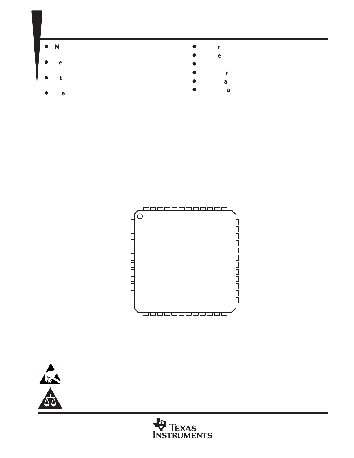
PFB PACKAGE
(TOP VIEW)
D
Power Amplifier Driver
D
Independent Power-Up/-Down Functions
D
3.75-V Operation
D
Low Current Consumption
D
Serial Data Interface
D
48-Pin Plastic Quad Flatpack (PFB)
TRF3520
CC
V
TXO_
47 46 45 44 4348 42
TXO_TNK2
TXO_TNK1
TXO_GND
PSUB
DRV_GND
DRV_OUT–
DRV_OUT+
DRV_GND
NC
NC
NC
NC
1
2
3
4
5
6
7
8
9
10
11
12
13
14 15
DRV_GND
NC – No internal connection
TXO_GND
TXO_SYNNCDB2_GND
17 18 19 20
16
NC
CC
V
VBG_IN
DRV_
DRV_GND
CC
CC
V
V
DIG_
DB2_OUT
DB2_
40 39 3841
21
I+
NC
VBG_OUT
DIG_CLK
DIG_STR
DIG_DAT
37
22 23 24
I–
Q+
MOD_GND
DIG_GND
TXM_V
36
TXM_GND
35
TXM_LO+
34
33
TXM_LO–
32
TXM_GND
TXM_GND
31
NC
30
PH2
29
PH1
28
MOD_GND
27
MOD_V
26
MOD_GND
25
Q–
CC
CC
These devices have limited built-in ESD protection. The leads should be shorted together or the device placed in conductive foam
during storage or handling to prevent electrostatic damage to the gates.
Please be aware that an important notice concerning availability, standard warranty, and use in critical applications of
Texas Instruments semiconductor products and disclaimers thereto appears at the end of this data sheet.
PRODUCTION DATA information is current as of publication date.
Products conform to specifications per the terms of Texas Instruments
standard warranty. Production processing does not necessarily include
testing of all parameters.
POST OFFICE BOX 655303 • DALLAS, TEXAS 75265
Copyright 1998, Texas Instruments Incorporated
1
TRF3520
GSM RF MODULATOR/DRIVER AMPLIFIER
SLWS060A – MAY 1998
functional block diagram
I +
I –
Q +
Q –
TXM_LO+
TXM_LO–
20
21
23
24
External
Tank
34
33
TXO_TNK2
1
Transmit
2
TXO_TNK1
90°
IF VCO
0°
I/Q Modulator
Buffer
Limiter
÷ 2
∑
Band-Pass
Filter (BPF)
Buffer
Low-Pass
Filter (LPF)
Power
Amplifier
Driver
46
To SYNTH
(TXO_SYN)
43
+
–
Divide
(DB2_OUT)
DRV_OUT+ 11
DRV_OUT– 10
Single-Sideband
Transmit Mixer
Buffer
-by-Two
Output
To External
Band
-Pass Filter,
Power Amplifier,
and Duplexer
Serial Interface
41 40 39 38 37
CC
DIG_V
DIG_CLK
DIG_DAT
DIG_STR
DIG_GND
transmit IF VCO
The transmit intermediate frequency (IF) VCO generates a CW signal in the 200-MHz range. The IF VCO
frequency is controlled by applying voltage to the required external tank varactors. Through on-chip buffers, the
transmit IF VCO output is sent to the SSB transmit mixer and divide-by-two functional blocks, as well as to an
external synthesizer where the transmit IF VCO frequency is controlled and phase locked. The error signal
generated by the synthesizer is sent to the transmit IF VCO varactors’ tuning port, completing the phase-locked
loop (PLL) function. The VCO is characterized for operation in the 74-MHz to 494-MHz range.
divide-by-two
This functional block halves the IF VCO frequency and provides a buffered amplitude-limited and low-pass
filtered signal, which can become the LO signal for the TRF1020 GSM Receiver IC second down-conversion
stage.
single-sideband transmit mixer (SSB Tx)
The SSB Tx mixer combines an external LO signal with the on-chip transmit IF VCO and performs a
down-conversion function. The SSB Tx mixer suppresses the undesired upper sideband signal that is typically
generated under the normal mixing process. An internal band-pass filter at the SSB Tx mixer output further
reduces the undesired sideband and any spurious signals. This function eliminates the use of any external
filtering. The LO is characterized for operation in the 990-MHz to 1400-MHz range.
I/Q modulator
The modulator provides direct I/Q modulation from baseband to RF . The differential baseband I/Q input signals
also provide DC bias to the modulator. A nominal DC voltage of 1.35 V at the I and Q ports is required. Other
types of complex I/Q modulations are possible with the TRF3520, but the device is optimized to meet GSM
requirements.
2
POST OFFICE BOX 655303 • DALLAS, TEXAS 75265
GSM RF MODULATOR/DRIVER AMPLIFIER
SLWS060A – MAY 1998
power amplifier driver output
The I/Q modulator output is fed to the power amplifier driver, which is a high-gain, low-distortion, fixed gain
amplifier. Its dif ferential output can be converted to single-ended by a simple LC impedance-matching network
and a 4:1 balun.
serial control interface
The serial control interface provides power-up and power-down capabilities for each of the functional blocks
described in the previous paragraphs.
The TRF3520 device register is manipulated using a synchronous serial data port. The timing relationships are
defined in Figure 1. One 17-bit word is clocked into a temporary holding register with the least significant bit
clocked first. The operation register is loaded with the new data residing in the temporary registers using the
rising edge of the strobe input.
The format of the control word is described in Table 1. Bits zero through two are reserved for future use. Bits
three through seven are power conservation bits. Bits eight through 16 are reserved.
Table 1. Control Word Bit Assignments
BIT FUNCTION FUNCTIONAL IF
0 Reserved –
1 Reserved –
2 Reserved –
3 Transmit oscillator and buffer amplifiers 1
4 Transmit mixer, LO buffer amplifier 1
5 Modulator 1
6 PA driver amplifier 1
7 Divide-by-two and limiter 1
8 Reserved –
9 Reserved –
10 Reserved –
11 Reserved –
12 Reserved –
13 Reserved –
14 Reserved –
15 Reserved –
16 Reserved –
TRF3520
POST OFFICE BOX 655303 • DALLAS, TEXAS 75265
3
TRF3520
I/O
DESCRIPTION
GSM RF MODULATOR/DRIVER AMPLIFIER
SLWS060A – MAY 1998
Terminal Functions
TERMINAL
NAME NO.
DB2_GND 44 – Divide-by-two circuitry ground
DB2_OUT 43 O Divide-by-two frequency output
DB2_V
CC
DIG_CLK 40 I Digital clock input
DIG_DAT 38 I Digital serial data input
DIG_GND 37 – Digital ground
DIG_STR 39 I Data strobe
DIG_V
CC
DRV_GND 9, 12, 13, 15 PA driver ground
DRV_OUT+ 11 O PA driver noninverting output
DRV_OUT– 10 O PA driver inverting output
DRV_V
CC
MOD_GND 22, 25, 27 Modulator ground
I+ 20 I Noninverting in-phase input
I– 21 I Inverting in-phase input
Q+ 23 I Noninverting quadrature input
Q– 24 I Inverting quadrature input
MOD_V
CC
NC 4, 5, 6, 8, 16,18, 30, 45 No internal connection
PSUB 7
TXO_GND 3, 47 – Transmit VCO ground
TXO_SYN 46 O Buffered transmit VCO output
TXO_TNK1 2 – Transmit VCO tank connection 1
TXO_TNK2 1 – Transmit VCO tank connection 2
TXO_V
CC
TXM_GND 31 – Transmit mixer ground
TXM_GND 32 – Transmit mixer ground
TXM_GND 35 – Transmit mixer ground
TXM_LO+ 34 I Transmit mixer LO noninverting input
TXM_LO– 33 I Transmit mixer LO inverting input
TXM_V
CC
PH1 28 – Phase adjustment resistor 1
PH2 29 – Phase adjustment resistor 2
VBG_IN 17 Band gap input
VBG_OUT 19 Band gap output
42 – Divide-by-two circuitry bias supply
41 – Digital supply
14 – PA driver bias supply
26 – Modulator supply
48 – Transmit VCO supply
36 – Transmit mixer supply
4
POST OFFICE BOX 655303 • DALLAS, TEXAS 75265
TRF3520
GSM RF MODULATOR/DRIVER AMPLIFIER
SLWS060A – MAY 1998
absolute maximum ratings over operating free-air temperature range (unless otherwise noted)
Supply voltage range: V
CC
Input voltage to any other pin: VIN –0.3 V to (VCC + 0.3) V. . . . . . . . . . . . . . . . . . . . . . . . . . . . . . . . . . . . . . . . . . .
Power dissipation, T
Maximum operating junction temperature: T
= 25°C, 48-pin PQFP 600 mW. . . . . . . . . . . . . . . . . . . . . . . . . . . . . . . . . . . . . . . . . . . . . . . . .
A
Jmax
Operating ambient temperature range –40°C to 85 °C. . . . . . . . . . . . . . . . . . . . . . . . . . . . . . . . . . . . . . . . . . . . . . .
Storage temperature range –65°C to 150 °C. . . . . . . . . . . . . . . . . . . . . . . . . . . . . . . . . . . . . . . . . . . . . . . . . . . . . . .
†
Stresses beyond those listed under “absolute maximum ratings” may cause permanent damage to the device. These are stress ratings only, and
functional operation of the device at these or any other conditions beyond those indicated under “recommended operating conditions” is not
implied. Exposure to absolute-maximum-rated conditions for extended periods may affect device reliability.
–0.3 V to 5.5 V. . . . . . . . . . . . . . . . . . . . . . . . . . . . . . . . . . . . . . . . . . . . . . . . . . . . . . . . .
150°C. . . . . . . . . . . . . . . . . . . . . . . . . . . . . . . . . . . . . . . . . . . . .
recommended operating conditions
MIN MAX UNIT
HIgh-level input voltage, V
Low-level input voltage, V
Supply voltage, V
Operating free-air temperature,T
CC
IH
IL
A
typical power consumption at 3.75 V (continuous operation)
MODULE OPERATING CURRENT STANDBY CURRENT OPERATING POWER STANDBY POWER
Transmit oscillator 8 mA <10 µA 30 mW <38 µW
Transmit mixer (SSBM) 50 mA <10 µA 188 mW <38 µW
Modulator 18 mA
PA driver amplifier 45 mA <10 µA 169 mW <38 µW
Divide-by-two + LPF 10 mA <10 µA 38 mW <38 µW
Control logic 50 µA
Total 131 mA <50 µA 492 mW <152 µW
2.0 V
CC
–0.3 0.8 V
3.6 3.9 V
–40 85 °C
V
†
POST OFFICE BOX 655303 • DALLAS, TEXAS 75265
5
TRF3520
DC current
GSM RF MODULATOR/DRIVER AMPLIFIER
SLWS060A – MAY 1998
electrical characteristics over recommended operating free-air temperature range (unless
otherwise noted)
transmit IF VCO VCC = 3.75 V, TA = 25°C, ZO = 100 Ω (unless otherwise noted)
PARAMETER
Frequency range 141 194 247 MHz
Output power (See Note 1) Z
Phase noise 200-kHz offset –110 dBc/Hz
Power-up time (See Note 2) 10 µs
Power-down time 10 µs
NOTES: 1. Measured at buffer output pin labeled TXO_SYN
2. Includes oscillator starting time. This time is measured starting at strobe transition to high; there is additional time after a reset, i.e.,
applying VCC to the circuit.
TEST
CONDITIONS
= 100 Ω –20 –15 dBm
load
Active mode 8 mA
Standby mode 10 µA
MIN TYP MAX UNIT
6
POST OFFICE BOX 655303 • DALLAS, TEXAS 75265

TRF3520
dBc
GSM RF MODULATOR/DRIVER AMPLIFIER
SLWS060A – MAY 1998
transmit mixer, I/Q modulator and PA driver PLO = –10 dBm, VCC = 3.75 V , TA = 25°C, ZO = 50 Ω (unless
otherwise specified)
PARAMETER
LO input frequency range 1070 1110 MHz
LO input power level –12 –10 –8 dBm
PA driver RF output 880 915 MHz
PA driver RF output power level See Note 7 6 dBm
Unwanted TX mixer sideband suppression at 1462 to 1497 MHz LO = 1074 to 1109 MHz 35 45 dBc
DSB IM suppression Third order See Note 3 20 dBc
Carrier suppression See Note 4 30 35 dBc
Sideband suppression See Note 4 35 45 dBc
100 kHz to 500 MHz See Note 5 35
500 to 850 MHz See Note 5 30 32
880 to 915 MHz Offset w600 kHz (see Note 5) 69
925 to 935 MHz See Note 5 85
935 to 960 MHz See Note 5 82
Modulator and P A driver spurious outputs
I/Q input voltage range (differential) Each differential line 0.0 1.80 V
I/Q offset 5 mV
I/Q common mode voltage See Note 6 1.25 1.35 1.45 V
I/Q input impedance (differential) See Note 8 10 kΩ
I/Q input impedance (single–ended) See Note 8 10 kΩ
I/Q input frequency range 0 2 MHz
Power-up time 10 µs
Power-down time 10 µs
PA driver output broadband noise
NOTES: 3. F
= 880 to 915 MHz, V
out
sideband level
4. F
= 880 to 915 MHz, V
out
with respect to desired sideband level
5. V
= 1.40 Vpp, 67.7 kHz sinewave. I & Q in quadrature-phase.
I/Q
6. The TCM4400 provides for a common-mode voltage of 1.35 ± 0.1 V or VCC/2 (software selectable)
7. Includes 1-dB loss associated with external balun
8. Specified by design.
I/Q
960 to 1000 MHz See Note 5 49
1000 to 1350 MHz See Note 5 30 39
1350 to 1500 MHz See Note 5 38
1500 to 1805 MHz See Note 5 23
1805 to 1880 MHz See Note 5 54
1880 to 12000 MHz See Note 5 36
= 1.40 VPP, 67.7 kHz sine wave. I & Q in-phase. Intermodulation suppression with respect to desired
I/Q
= 1.40 VPP, 67.7 kHz sine wave. I & Q in quadrature-phase. Carrier and undesired sideband suppression
TEST CONDITIONS MIN TYP MAX UNIT
± 10 MHz,
PA driver output =+ 6 dBm
–131 dBc/Hz
PP
POST OFFICE BOX 655303 • DALLAS, TEXAS 75265
7

TRF3520
t
t
GSM RF MODULATOR/DRIVER AMPLIFIER
SLWS060A – MAY 1998
transmit mixer, I/Q modulator and PA driver PLO = –10 dBm, VCC = 3.75 V , TA = 25°C, ZO = 50 Ω (unless
otherwise specified) (continued)
divide-by-two V
Input frequency range 141 194 247 MHz
Output frequency F
Output power (see Note 8) Z
DC current Active mode 10 mA
DC current Standby mode 10 µA
NOTE 9: Measured at buf fer output pin labeled DB2_OUT
serial interface timing requirements with VCC = 3.75 V, TA = 25°C, Z
= 3.75 V, TA = 25°C, Zo=50 Ω (unless otherwise specified)
CC
PARAMETER
TEST CONDITIONS MIN TYP MAX UNIT
= 100 Ω –25 –20 –10 dBm
load
O
/2
DB2_IN
= 50 Ω (unless otherwise specified)
(see Figure 1)
PARAMETER TEST CONDITIONS MIN TYP MAX UNIT
R
i
f
clock
t
(r) t(f)
tw(High) Pulse duration, CLOCK high 20 ns
tw(Low) Pulse duration, CLOCK low 20 ns
su
h
t
w(pulse)
CLOCK, DATA and STROBE input resistance 10 kΩ
CLOCK frequency 0 20 MHz
CLOCK input rise and fall time 8 ns
Data setup time before CLOCK high 20 ns
Strobe setup time before CLOCK high 20 ns
Data hold time after CLOCK high 20 ns
Strobe hold time after CLOCK high 20 ns
Strobe pulse width duration
2
REF_IN
ns
DATA
CLOCK
STROBE
PARAMETER MEASUREMENT INFORMATION
Data
Valid
D0 D1 D22 D23
Data
Change
t
su
t
h
t
w(Low)
Clock Enabled
Shift in Data
t
w(High)
Figure 1. TRF3520 Timing Relationships
t
su
Clock Disabled
t
w(pulse)
Store Data
– V
IH
– V
IL
– V
IH
– V
– V
– V
IL
IH
IL
t
h
8
POST OFFICE BOX 655303 • DALLAS, TEXAS 75265

TRF3520
GSM RF MODULATOR/DRIVER AMPLIFIER
SLWS060A – MAY 1998
TYPICAL CHARACTERISTICS
Typical GSM RF modulator characteristics were evaluated using a VCO frequency of 194 MHz and LO
frequency of 1094 MHz. The range of operation is specified in the document and is therefore customer specific.
PA DRIVER OUTPUT POWER
TEMPERATURE
9
8
7
6
5
PA Driver Output Power – dBm
4
3
–60 –40 –20 0 20 40
VCC = 3.9 V
T – Temperature – °C
Figure 2
PA DRIVER OUTPUT POWER
LO POWER
8.5
8
7.5
7
vs
VCC = 3.75 V
VCC = 3.6 V
vs
–40°C
25°C
60 80 100
PA DRIVER OUTPUT POWER
LO FREQUENCY
9
8
7
6
5
PA Driver Output Power – dBm
4
3
1060 1070 1080 1090
LO Frequency – MHz
Figure 3
TOTAL SUPPLY CURRENT, I
TEMPERATURE
138
136
134
132
VCC = 3.75 V
vs
–40°C
25°C
85°C
1100 1110 1120
CC
vs
VCC = 3.9 V
6.5
6
5.5
5
PA Driver Output Power –dBm
4.5
4
–13 –11
LO Power In – dBm
85°C
Figure 4
130
128
– Total Supply Current – mAI
126
CC
124
122
–9 –7
POST OFFICE BOX 655303 • DALLAS, TEXAS 75265
120
–50 0
T – Temperature – °C
VCC = 3.6 V
50 100
Figure 5
9

TRF3520
GSM RF MODULATOR/DRIVER AMPLIFIER
SLWS060A – MAY 1998
TYPICAL CHARACTERISTICS
CARRIER SUPPRESSION
TEMPERATURE
–38
VCC = 3.9 V
–37
–36
VCC = 3.6 V
Carrier Suppression – dBc
–35
–34
–60 –40 –20 0 20 40
T – Temperature – °C
Figure 6
CARRIER SUPPRESSION
LO FREQUENCY
40
vs
VCC = 3.75 V
vs
60 80 100
CARRIER SUPPRESSION
LO INPUT POWER
38
37
36
35
Carrier Suppression – dBc
34
–13 –12 –11 –10
LO Input Power – dBm
Figure 7
CARRIER SUPPRESSION
I/Q DC OFFSET
38
vs
–40°C
25°C
85°C
–9 –8 –7
vs
39
38
37
36
35
Carrier Suppression – dBc
34
33
1065 1075 1085 1095
LO Frequency – MHz
Figure 8
–40°C
25°C
85°C
1105 1115
37
36
35
Carrier Suppression – dBc
34
1.2 1.25 1.3 1.35 1.4 1.45 1.5
–40°C
25°C
85°C
1.55 1.6 1.65 1.7
I/Q DC Offset – V
Figure 9
10
POST OFFICE BOX 655303 • DALLAS, TEXAS 75265

GSM RF MODULATOR/DRIVER AMPLIFIER
TYPICAL CHARACTERISTICS
TRF3520
SLWS060A – MAY 1998
DSB IM SUPPRESSION
LO FREQUENCY
29.5
29
28.5
28
27.5
27
26.5
26
25.5
DSB IM Suppression – dBc
25
24.5
24
1060 1070 1080 1090
85°C
–40°C
25°C
LO Frequency – MHz
Figure 10
SIDEBAND SUPPRESSION
LO FREQUENCY
48
vs
1100 1110 1120
vs
SIDEBAND SUPPRESSION
TEMPERATURE
–48
–46
–44
–42
–40
–38
Sideband Suppression – dBc
–36
–34
VCC 3.9 V
VCC 3.75 V
VCC 3.6 V
–50 0
T – Temperature – °C
Figure 11
SIDEBAND SUPPRESSION
LO INPUT POWER
48
vs
50 100
vs
46
44
42
40
38
36
Sideband Suppression – dBc
34
32
1060 1080
–40°C
25°C
85°C
LO Frequency – MHz
Figure 12
1100 1120
46
44
42
40
38
36
Sideband Suppression – dBc
34
32
–13 –11
LO Input Power – dBm
Figure 13
–40°C
25°C
85°C
–9 –7
POST OFFICE BOX 655303 • DALLAS, TEXAS 75265
11

TRF3520
GSM RF MODULATOR/DRIVER AMPLIFIER
SLWS060A – MAY 1998
TYPICAL CHARACTERISTICS
LO FEEDTHROUGH TO DRV_OUT
TEMPERATURE
–38
–39
–40
–41
–42
–43
LO Feedthrough to DRV_OUT – dBc
–44
–60 –40 –20 0 20 40
T – Temperature – °C
Figure 14
vs
VCC = 3.75 V
–16
VCC = 3.9 V
VCC = 3.6 V
60 80 100
–10
–10.5
11
–11.5
–12
VCO Output Power – dBm
–12.5
–13
–60 –40 –20 0 20 40
DB2 OUTPUT POWER
vs
TEMPERATURE
VCO OUTPUT POWER
TEMPERATURE
VCC = 3.9 V
VCC = 3.6 V
T – Temperature – °C
Figure 15
vs
VCC = 3.75 V
60 80 100
–16.5
–17
–17.5
–18
–18.5
DB2 Output Power – dBm
–19
–19.5
–20
–60 –40 –20 0 20 40
T – Temperature – °C
VCC = 3.6 V
VCC = 3.75 V
VCC = 3.9 V
60 80 100
Figure 16
12
POST OFFICE BOX 655303 • DALLAS, TEXAS 75265

GSM RF MODULATOR/DRIVER AMPLIFIER
SLWS060A – MAY 1998
APPLICATION INFORMATION
Table 2. TRF3520 Application Board Parts List
DESIGNATORS DESCRIPTION VALUE QTY SIZE MANUFACTURER MANUFACTURER P/N
C1, 2, 3, 15 Capacitor 10 pF 4 0603 Murata GRM39COG Series
C4, 5, 8, 10, 12,
14, 19, 32, 36, 37
C6, 23, 26, 30, 35 Capacitor 1000 pF 5 0603 Murata GRMX7R Series
C7, 9, 11, 25, 28,
29, 33, 34, 38
C13, 31 Capacitor 10 µF 2 C Panasonic ECS–T1DC106R
C16 Capacitor 22 pF 1 0603 Murata GRM39COG Series
C17 Capacitor 8 pF 1 0603 Murata GRM39COG Series
C18 Capacitor 7 pF 1 0603 Murata GRM39COG Series
C20, 22 Capacitor 15 pF 2 0603 Murata GRM39COG Series
C21 Capacitor 4.7 pF 1 0603 Murata GRM39COG Series
C24, 27 Capacitor 1.8 pF 2 0603 Murata GRM39COG Series
C39 Capacitor 1.5 pF 1 0603 Murata GRM39COG Series
L1 Inductor 100 nH 1 0603 Toko LL1608–FR10K
L2 Inductor 47 nH 1 0603 Toko LL1608–F47NK
L3 Inductor 56 nH 1 0603 Toko LL1608–F56NK
L4, 5 Inductor 6.8 nH 2 0603 Toko LL1608–F6N8K
J1, 3, 5, 6, 11 SMA connector 5 EF Johnson 142–0701–801
J2 Connector 1 Amp 747250–4
P1, P2, P3 Connector 3 Molex 46F522
J7, 8, 9, 10 BNC connector 4 Amp 413631–1
R2, 4, 6 Resistor 1.0 k
R3 ,5, 7 Resistor 1.5 k
R8, 9, 10, 12, 18,
20
R13, 14 Resistor 220 2 0603 Panasonic P220GCT–ND
R15, 16 Resistor 47 k
R22 Resistor 2 k
U1 IC 1 TI TRF3520
Varactor Varactor 2 Motorola MMBV2109LT1
T1 4:1 Balun 1 MA/COM ETC1.6–4–2–3
Capacitor .01 µF 10 0603 Murata GRM39COG Series
Capacitor 100 pF 9 0603 Murata GRM1R8X7R Series
W
W
Resistor 0 6 0603 Panasonic P0.0GCT–ND
W
W
3 0603 Panasonic P1.0KGCT–ND
3 0603 Panasonic P1.5KGCT–ND
2 0603 Panasonic P47KGCT–ND
1 0603 Digikey P2.0KGCT–ND
TRF3520
POST OFFICE BOX 655303 • DALLAS, TEXAS 75265
13

TRF3520
GSM RF MODULATOR/DRIVER AMPLIFIER
SLWS060A – MAY 1998
APPLICATION INFORMATION
J1
SMA
J2:B
J2:E
J2:C
J3
SMA
J2:I
DIG_VCC
2
5
3
9
DB2_OUT
TXO_SYN
VCC
C16
22 pF
R2
1 k
R4
1 k
R6
1 k
VCC
R9
0
1.5 k
C15
10 pF
R7
C17
8.0 pF
47 nH
P3
P2
C3
10 pF
100 nH
L2
1
2
1
2
L1
R5
1.5 k
7.0 pF
.01 µ F
.01 µ F
C18
C32
C14
R13
220
C2
10 pF
TP1
+
10 µ F
1.5 k
R14
+
C31
10 µ F
C13
R3
DIG_VCC
220
C1
10 pF
C4
.01 µ F
WORD_OUT
1
C19
.01 µ F
VCC
R8
0
C36
.01 µ F
C5
.01 µ F
TXM_LO
C29
VCC
.01 µ F
C37
.01 µ F
C35C6
1000 pF1000 pF
C20
15 pF
3113
R15
47 k
C23
1000 pF
100 pF
C11C12
100 pF
37
38
39
40
41
42
43
44
45
46
47
48
L3
56 nH
C21
4.7 pF
CR2CR1
MMBV2109MMBV2109
1
P1
2
C30
1000 pF
3635343332313029282726
U1
TRF3520
123456789
TP2
C22
15 pF
R16
47 k
VCO_TUNE
J5
SMA
J11
SMA
25
101112
L4 L5
6.8 nH 6.8 nH
C38
100 pF
C10
.01
24
23
22
21
20
19
18
17
16
15
14
13
C25
100 pF
µ F
C9
100 pF
R 22
2 k
C7
100 pFC8.01
C27
1.8 pF
C24
1.8 pF
C26
1000 pF
VCC
C33
100 pF
R10
R11
DNP
R12
R17
DNP
R18
R19
DNP
R20
R21
µ F
34
2
1
ECT 1.6–4–2–3
VCC
Q–
C34
Q+
I–
I+
100 pF
5
VCC
C28
J10
BNC
J9
BNC
J8
BNC
J7
BNC
DRV_OUT
1.5 pF
0
0
0
0
100 pF
R11, R17, R19, R21 =
DNP (DO NOT PLACE)
C39
J6
SMA
Figure 17. TRF3520 Application Board Schematic
14
POST OFFICE BOX 655303 • DALLAS, TEXAS 75265

TRF3520
GSM RF MODULATOR/DRIVER AMPLIFIER
SLWS060A – MAY 1998
APPLICATION INFORMATION
The TRF3520 combines RF, IF , and digital signals. In order to obtain maximum performance, follow correct RFpwb
layout procedures.
J11
TRF3520 DEMO BOARD, EVM REV: A
TXM_LO
COPYRIGHT: TEXAS INS. 1998
P3
C31
+
P2
C13
+
C14C32
R9
J10
R11
R10
Q–
J1
J3
J5
VCO_TUNE
J2
DB2_OUT
TXO_SYN
C11
C28
C38
C10
C33
U1
C16L1C15
R13
C38
C37
C19
C36
L2
R14
C18
C17
C20R15
CR2
C21
L3
C22
CR1
C23
R16
P1
R22
C8
C34
T1
C25
C24
L5
C26
C27
C28
C39
DRV_OUT
L4
C38
J6
Figure 18. TRF3520 Application Board Layout
R17
Q+
R19
I–
R21
I+
J9
R12
J8
R18
J7
R20
POST OFFICE BOX 655303 • DALLAS, TEXAS 75265
15

TRF3520
GSM RF MODULATOR/DRIVER AMPLIFIER
SLWS060A – MAY 1998
MECHANICAL DATA
PFB (S-PQFP-G48) PLASTIC QUAD FLATPACK
37
48
1,05
0,95
0,50
36
0,27
0,17
25
24
13
1
5,50 TYP
7,20
SQ
6,80
9,20
SQ
8,80
12
M
0,08
0,05 MIN
Seating Plane
0,13 NOM
Gage Plane
0,25
0°–7°
0,75
0,45
1,20 MAX
NOTES: A. All linear dimensions are in millimeters.
16
B. This drawing is subject to change without notice.
C. Falls within JEDEC MS-026
POST OFFICE BOX 655303 • DALLAS, TEXAS 75265
0,08
4073176/B 10/96

IMPORTANT NOTICE
T exas Instruments and its subsidiaries (TI) reserve the right to make changes to their products or to discontinue
any product or service without notice, and advise customers to obtain the latest version of relevant information
to verify, before placing orders, that information being relied on is current and complete. All products are sold
subject to the terms and conditions of sale supplied at the time of order acknowledgement, including those
pertaining to warranty, patent infringement, and limitation of liability.
TI warrants performance of its semiconductor products to the specifications applicable at the time of sale in
accordance with TI’s standard warranty. Testing and other quality control techniques are utilized to the extent
TI deems necessary to support this warranty . Specific testing of all parameters of each device is not necessarily
performed, except those mandated by government requirements.
CERTAIN APPLICA TIONS USING SEMICONDUCT OR PRODUCTS MAY INVOLVE POTENTIAL RISKS OF
DEATH, PERSONAL INJURY, OR SEVERE PROPERTY OR ENVIRONMENTAL DAMAGE (“CRITICAL
APPLICATIONS”). TI SEMICONDUCTOR PRODUCTS ARE NOT DESIGNED, AUTHORIZED, OR
WARRANTED TO BE SUITABLE FOR USE IN LIFE-SUPPORT DEVICES OR SYSTEMS OR OTHER
CRITICAL APPLICA TIONS. INCLUSION OF TI PRODUCTS IN SUCH APPLICATIONS IS UNDERST OOD TO
BE FULLY AT THE CUSTOMER’S RISK.
In order to minimize risks associated with the customer’s applications, adequate design and operating
safeguards must be provided by the customer to minimize inherent or procedural hazards.
TI assumes no liability for applications assistance or customer product design. TI does not warrant or represent
that any license, either express or implied, is granted under any patent right, copyright, mask work right, or other
intellectual property right of TI covering or relating to any combination, machine, or process in which such
semiconductor products or services might be or are used. TI’s publication of information regarding any third
party’s products or services does not constitute TI’s approval, warranty or endorsement thereof.
Copyright 2000, Texas Instruments Incorporated
 Loading...