

Page 1
AGC
CNTL
7
0/90TXPLL
3
RXAGC
VCCs
GNDs
RXPLL
TXQ_IN
TX_OUT
TXI_IN
RX_IN
RX VGA
TX VGA
IFAMP
From SPI
from RXPLL
XPIC_IN
XPIC
OUT
XPIC
AGC
XPIC_BBI
XPIC_BBQ
Level
Detect
IF SAW
IF_OUT
IF_IN
TX_PWD
Temperature
Sensor
CLKSPI
DATASPI
LESPI
RXBBI
RXBBQ
TEMPOUT
0/90
0/90
S
P
I
User's Guide
SLWU065 – September 2009
TRF2443 Integrated IF Transceiver Evaluation Module
This document provides an easy guide for evaluating the TRF2443 integrated IF transceiver for broadband
wireless applications. Included in this guide are equipment setup procedures, software GUI configurations,
and test procedures that allow a user to quickly and accurately measure the TRF2443 performance.
The TRF2443 is a fully integrated IF transceiver operating at a transmitter IF of 340 MHz (or 170 MHz)
and a receiver IF of 140 MHz (or 280MHz). The IF transceiver is used to for up-conversion of signals from
the transmit chain digital-to-analog convertor (DAC) to the RF upconverter device and for
down-conversion of received IF signals to baseband for processing by the analog-to-digital convertor
(ADC). The receiver allows for switching in an external SAW filter if needed or by-passing this filter and
processing the signal completely internally. The TRF2443 also provides an Auxiliary Receiver which can
be used for cross-polarization interference cancellation (XPIC). This document describes how to test the
TRF2443 as well as the many options for trimming the device configuration to meet your application
needs.
SLWU065 – September 2009 TRF2443 Integrated IF Transceiver Evaluation Module 1
Submit Documentation Feedback
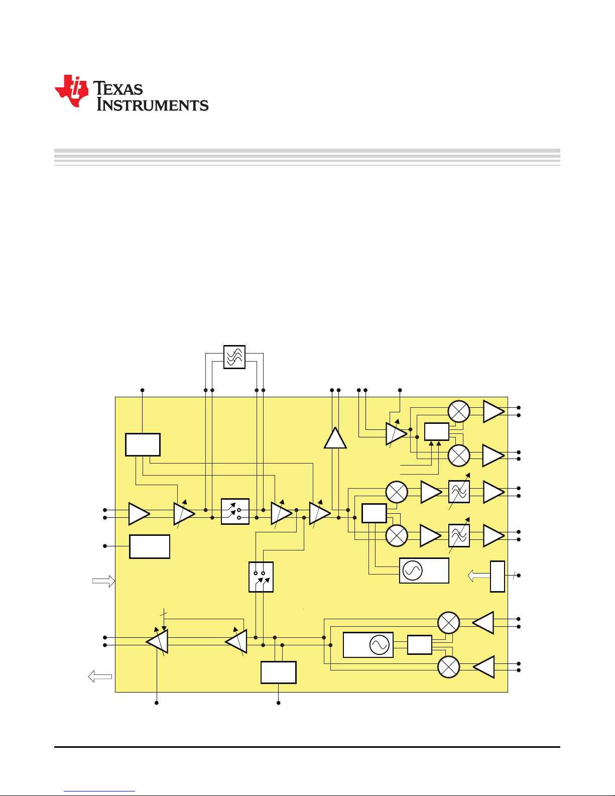
Figure 1. TRF2443 Block Diagram
Page 2

www.ti.com
Contents
1 EVM Circuit Overview ....................................................................................................... 4
1.1 DC POWER ......................................................................................................... 4
1.2 Reference Clock .................................................................................................... 5
1.3 Communications .................................................................................................... 5
1.4 Transmitter ........................................................................................................... 5
1.5 Receiver .............................................................................................................. 6
1.6 XPIC Receiver....................................................................................................... 9
2 GUI Overview ............................................................................................................... 10
2.1 GUI for Synthesizers .............................................................................................. 12
2.2 GUI for Receiver ................................................................................................... 14
2.3 GUI Transmitter.................................................................................................... 15
2.4 GUI for XPIC Receiver ........................................................................................... 15
3 TRF2443 EVM Operating Procedures ................................................................................... 16
3.1 Power Up ........................................................................................................... 16
3.2 Receiver ............................................................................................................ 17
3.3 XPICOUT Amplifier ............................................................................................... 18
3.4 Transmitter ......................................................................................................... 19
3.5 EEPROM ........................................................................................................... 20
3.6 XPIC RECEIVER .................................................................................................. 21
4 Physical Description ....................................................................................................... 23
4.1 EVM Top Layer Drawing ......................................................................................... 23
4.2 Bill of Materials .................................................................................................... 24
4.3 Schematics ......................................................................................................... 26
List of Figures
1 TRF2443 Block Diagram .................................................................................................... 1
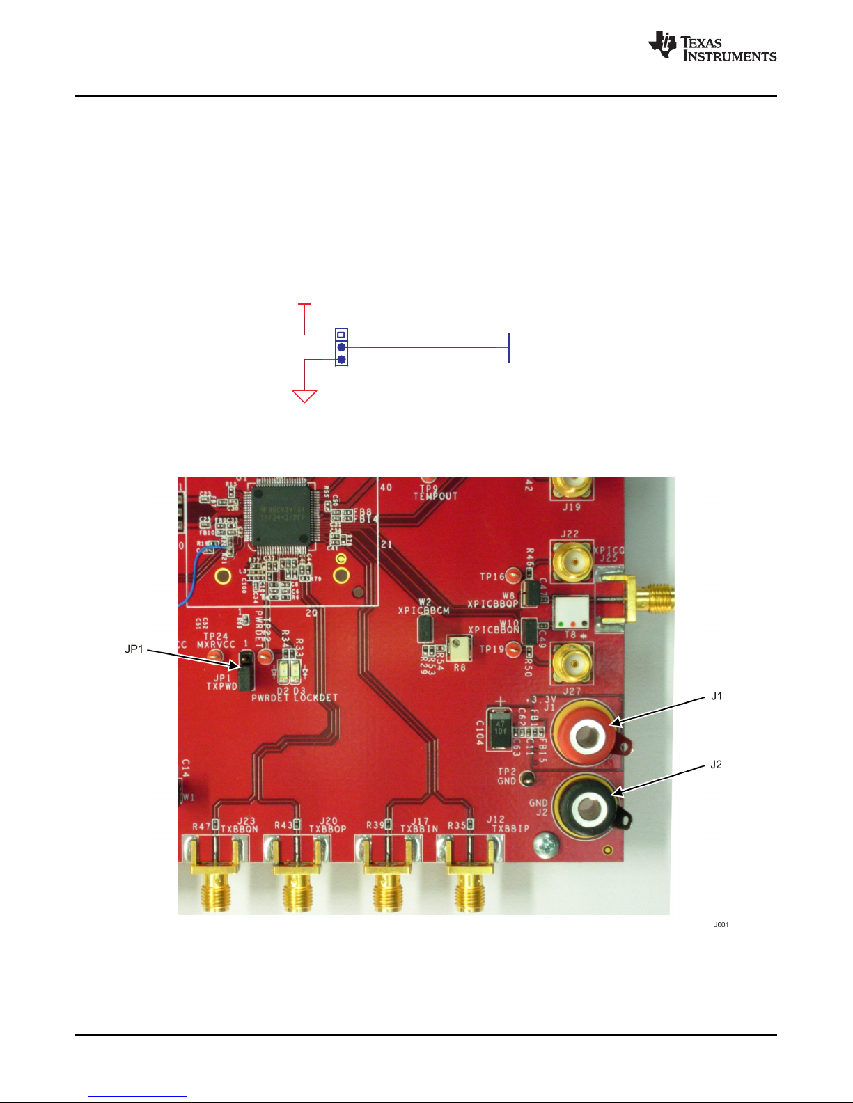
2 TXPWD Header JP1 Schematic ........................................................................................... 4
3 EVM DC Power: J1, J2, and JP1 .......................................................................................... 4
4 EVM Reference Clock J3 and USB Port J5 .............................................................................. 5
5 TX Baseband Inputs ......................................................................................................... 6
6 J7 (RXIN) ..................................................................................................................... 6
7 RX Baseband Outputs ...................................................................................................... 7
8 SAW Filter Path .............................................................................................................. 8
9 XPIC RX ...................................................................................................................... 9
10 TRF2443 GUI Quick-Set Tab ............................................................................................. 10
11 TRF2443 GUI Advanced Tab ............................................................................................. 11
12 Load All Registers .......................................................................................................... 12
13 Reset USB .................................................................................................................. 12
14 Synthesizer Programming ................................................................................................. 12
15 RX GUI ...................................................................................................................... 14
16 RX AGC GUI ................................................................................................................ 14
17 Transmitter GUI............................................................................................................. 15
18 XPIC Receiver GUI ........................................................................................................ 15
19 XPIC AGC GUI ............................................................................................................. 15
20 Programmed ICC GUI Settings ........................................................................................... 16
21 Load All Registers .......................................................................................................... 16
22 Receiver SAW Disabled GUI Settings ................................................................................... 17
23 Receiver SAW Enabled GUI Settings ................................................................................... 18
24 Receiver XPICOUT GUI Settings ........................................................................................ 19
25 TX Max Gain GUI Settings ................................................................................................ 19
26 GUI Settings for TX Carrier Leakage .................................................................................... 20
27 GUI Show Readback ...................................................................................................... 20
2 List of Figures SLWU065 – September 2009
Submit Documentation Feedback
Page 3

www.ti.com
28 GUI Select EEPROM Readback ......................................................................................... 20
29 Read I/Q Carrier Leakage Trim Values B < 10,5> ...................................................................... 21
30 TX Carrier Leakage Trim .................................................................................................. 21
31 XPIC Receiver Max Gain GUI ............................................................................................ 22
32 XPIC Receiver Min Gain GUI ............................................................................................. 22
33 TRF2443 EVM Top Layer ................................................................................................. 23
34 Schematic (1 of 5) .......................................................................................................... 26
35 Schematic (2 of 5) .......................................................................................................... 27
36 Schematic (3 of 5) .......................................................................................................... 28
37 Schematic (4 of 5) .......................................................................................................... 29
38 Schematic (5 of 5) .......................................................................................................... 30
List of Tables
1 Bill of Materials ............................................................................................................. 24
SLWU065 – September 2009 List of Tables 3
Submit Documentation Feedback
Page 4
GND
+3.3V
JP1
TXPWD
1
3
2
TXPWD
80
SHUNT 2-3
S006
EVM Circuit Overview
1 EVM Circuit Overview
1.1 DC POWER
The TRF2443 EVM requires a 3.3V dc power-supply connected to between J1 (3.3V) and J2 (GND). The
TRF2443 allows for analog or digital control of the transmitter power supply. Pin 1 (TXPWD) of the device
provides the analog control and is connected to header JP1 (TXPWD) on the EVM. When pins 1 and 2 of
header JP1 are shorted, 3.3V is fed to the TXPWD pin and the transmitter is disabled. When pins 2 and 3
of header JP1 are shorted, 0V is fed to the TXPWD pin and the transmitter is enabled (see Figure 2 and
Figure 3 ). With header JP1 enabling the transmitter, it is still possible for the transmitter to be off due to
the state of the digital TX control.
www.ti.com
Figure 2. TXPWD Header JP1 Schematic
List of Tables4 SLWU065 – September 2009
Figure 3. EVM DC Power: J1, J2, and JP1
Submit Documentation Feedback
Page 5
www.ti.com
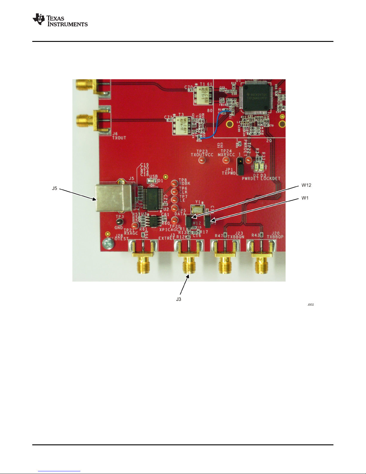
1.2 Reference Clock
The TRF2443 EVM allows for either an external reference chosen by the user or an internal oscillator at
20 MHz provided on the EVM board. If an external reference is to be used the signal should be fed into
SMA connector J3 (EXTREF) and jumpers W1 and W12 should be removed (see Figure 4 ).
EVM Circuit Overview
Figure 4. EVM Reference Clock J3 and USB Port J5
1.3 Communications
The EVM is equipped with USB communications which provide the interface between a computer's USB
port and the TRF2443s SPI port via J5 as shown in Figure 4 . A CD containing the GUI to control the
TRF2443 is provided within the EVM kit. An overview of the GUI is provided in this document
1.4 Transmitter
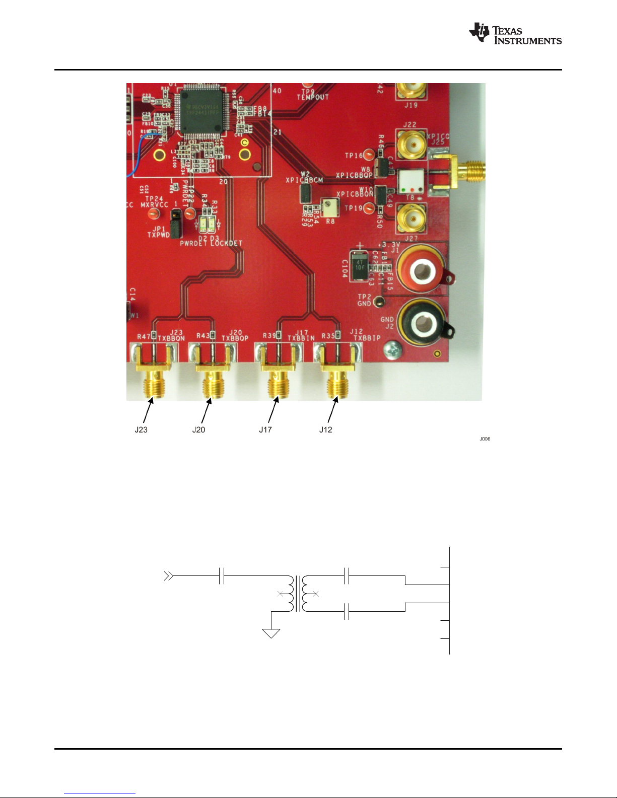
The EVM is configured for differential I/Q input signals via four SMA connectors. For the upper sideband,
the I signals are connected to J12 (TXBBIP) and J17 (TXBBIN). The Q signals are connected to J23
(TXBBQN) and J20 (TXBBQP) (see Figure 5 ). SMA connector J6 (TXOUT), not shown below, is used to
monitor the RF output signal from the transmitter.
SLWU065 – September 2009 List of Tables 5
Submit Documentation Feedback
Page 6
RXIN
50 OHM DIFF
50 OHM
220pF220pF
RXINP
68
RXINN
69
GNDRX
70
GNDRX
71
VCCRX
67
220pF
S007
EVM Circuit Overview
www.ti.com
1.5 Receiver
The EVM is configured for single ended RX input signal via SMA connector J7 (RXIN). This input is taken
through a 1:1 balun to provide differential inputs to the device. The device presents 50 so no external
termination resistor is required.
6 List of Tables SLWU065 – September 2009
Figure 5. TX Baseband Inputs
Figure 6. J7 (RXIN)
Submit Documentation Feedback
Page 7
www.ti.com
EVM Circuit Overview
The baseband I/Q signals can be measured balanced or unbalanced. The I output is taken from the
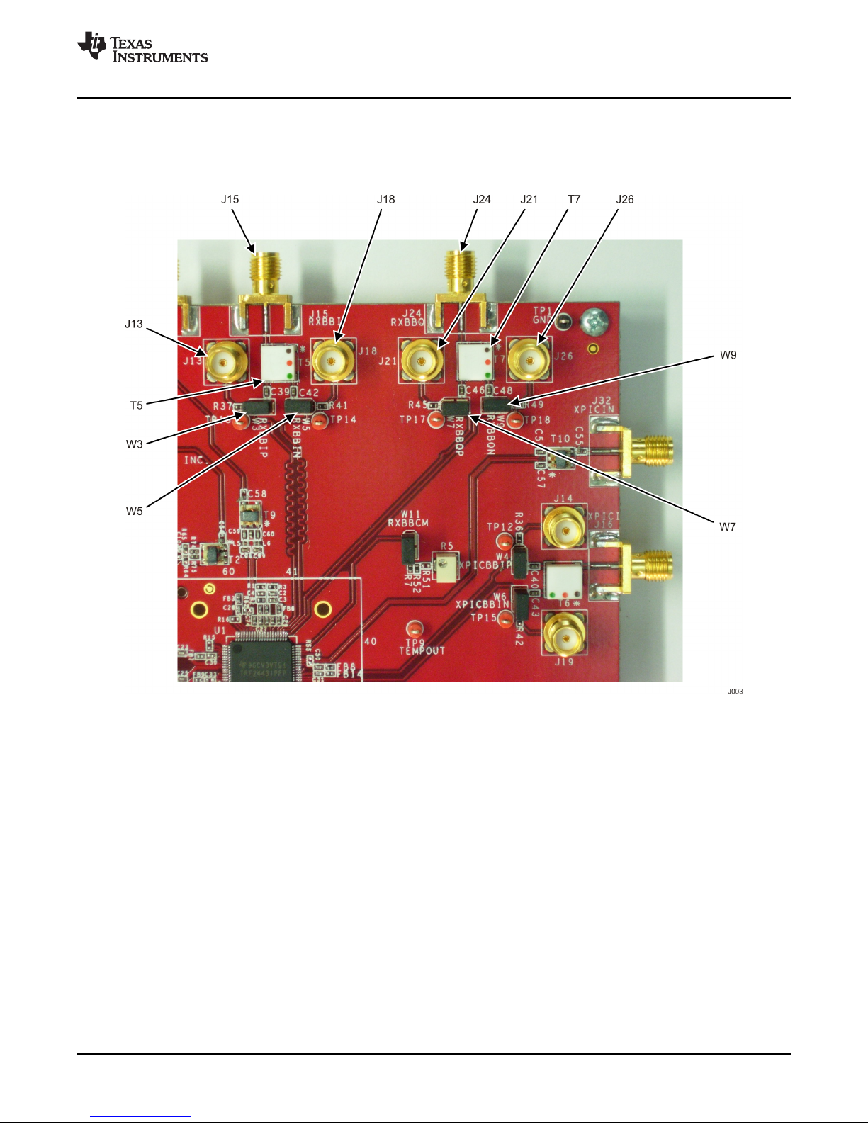
unbalanced port J15 (RXBBI) through balun T5 or from the balanced ports of J13 (I+) and J18 (I-).
Likewise, the Q output is taken from the unbalanced port J24 (RXBBQ) through balun T7 or the balanced
ports of J21 (Q+) and J26 (Q-). For balanced mode measurements, jumpers W3, W5, W7 and W9 must
be removed.
SLWU065 – September 2009 List of Tables 7
Submit Documentation Feedback
Figure 7. RX Baseband Outputs
Page 8
EVM Circuit Overview
www.ti.com
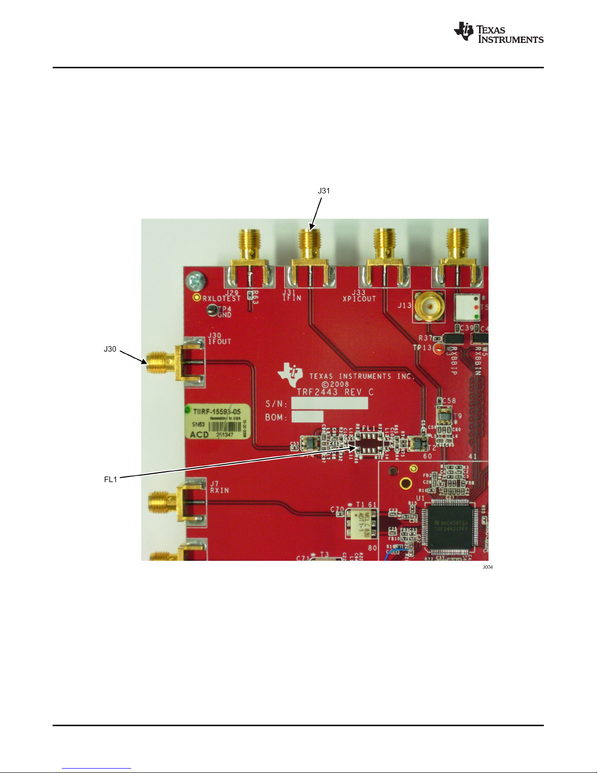
The TRF2443 RX path allows the use of an external SAW filter. An internal switch, which is programmable
through the serial interface, gives the flexibility to utilize the external filter (see Figure 1 ). The internal
switch is controlled via the serial programming interface through bit EN_SAW. By programming EN_SAW
to 1, the external path is selected, whereas a 0 engages the internal bypass switch. When EN_SAW is set
to 1 the IF signal will be routed out of the IC to SMA connector J30 (IFOUT) (see Figure 8 ). At this point,
the user has the flexibility to insert a filter of choice outside the TRF2443 EVM. (The board does contain a
place holder (FL1) for a SAW filter but is not populated. In this way, the user has the flexibility to use a
filter of his choice). For initial evaluation, an 8-10 dB pad can be used in lieu of a filter to emulate the
insertion loss of a typical filter. The user must route the signal from J30 (IFOUT) to J31 (IFIN) with the filter
or pad included.
List of Tables8 SLWU065 – September 2009
Figure 8. SAW Filter Path
Submit Documentation Feedback
Page 9
www.ti.com
1.6 XPIC Receiver
EVM Circuit Overview
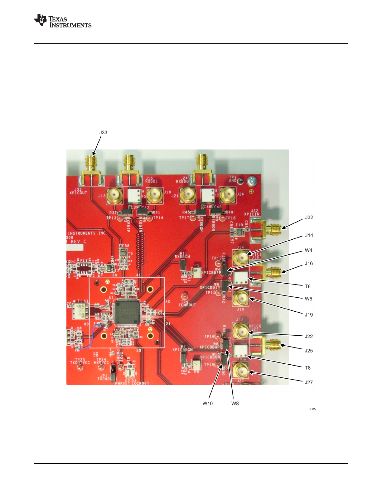
The TRF2443 provides an auxiliary receiver chain that can be used for cross-polarization interference
cancellation purposes. The EVM is configured for a single-ended output signal (intended for the secondary
XPIC RX path) at J33 (XPICOUT). The input to the XPIC receiver (from the XPICOUT of the secondary
XPIC RX path) is available at SMA connector J32 (XPICIN). This input is taken through a 1:1.5 balun to
provide differential inputs to the device. The device presents 75 so no external termination resistor is
required. The XPIC baseband I and Q signals can be measured balanced or unbalanced. The I output is
taken from the unbalanced port J16 (XPICI) through balun T6 or from the balanced ports of J14 (I+) and
J19 (I-). Likewise, the Q output is taken from the unbalanced port J25 (XPICQ) through balun T8 or the
balanced ports of J22 (Q+) and J27 (Q-). For balanced mode measurements, jumpers W4, W6, W8, and
W10 must be removed (see Figure 9 ).
SLWU065 – September 2009 List of Tables 9
Submit Documentation Feedback
Figure 9. XPIC RX
Page 10

GUI Overview
www.ti.com
2 GUI Overview
The TRF2443 EVM kit includes a graphical user interface for controlling the device. The GUI contains two
tabs labeled "Quick-set" and "Advanced" (see Figure 10 and Figure 11 )
10 List of Tables SLWU065 – September 2009
Figure 10. TRF2443 GUI Quick-Set Tab
Submit Documentation Feedback
Page 11

www.ti.com
GUI Overview
Evaluation and testing of the device can be done entirely using on the "Quick-set" tab. The "Advanced"
tab is used for debugging and specific optimization of the device if required by an application. Using the
"Advanced" tab without an understanding of what is being controlled can result in an unrecoverable state
of the IC whereby a power reset would be required.
SLWU065 – September 2009 List of Tables 11
Submit Documentation Feedback
Figure 11. TRF2443 GUI Advanced Tab
Page 12

GUI Overview
www.ti.com
When an input to the GUI is changed, the GUI should send this new value to the device automatically
once the cursor has clicked on another field besides the field being changed. It is good practice, however,
to reload all registers once changes to inputs have been made. This can be achieved by clicking on the
"OFF" button below "Load All" in the bottom right corner of the GUI (see Figure 12 ).
Figure 12. Load All Registers
If there is ever a doubt as to the integrity of the communications between the GUI and the device, a USB
reset is in order. Press the Reset USB button near the top left corner of the GUI and then reload all
registers again (see Figure 13 ).
Figure 13. Reset USB
An explanation of all the fields within the Quick-set tab is provided by device functionality beginning with
the synthesizers.
2.1 GUI for Synthesizers
The TX and RX synthesizers are controlled using the group of dialog boxes under "Quick-Synth" (see
Figure 14 ).
12 List of Tables SLWU065 – September 2009
Figure 14. Synthesizer Programming
Submit Documentation Feedback
Page 13

www.ti.com
GUI Overview
Ref Freq[MHz]
Specify the reference frequency being provided to the EVM. If the on-board oscillator is used, this will be
20MHz. If an external oscillator is to be used, specify its frequency in this field.
TX VCO [MHz]
This field is a calculation based on the other inputs provided. The TX VCO is guaranteed to operate
between 2640MHz and 2800MHz.
TX Freq. [MHz]
The TX LO Frequency can be programmed to a frequency within the TX Synth Range selected previously.
Entering a value outside of this range is not permitted and will default to the closest value within this
range. When TX Freq. is specified, the corresponding TX VCO will be calculated.
PFD_TX [MHz]
Specify the channel resolution desired of the LO by selecting the PFD frequency. Note that the PLL loop
filters are optimized for a PFD frequency of 20MHz. Deviating from 20MHz will impact the phase noise of
the system.
RX VCO [MHz]
This field is a calculation based on the other inputs provided. The RX VCO is guaranteed to operate
between 2240MHz and 2640MHz.
RX Freq. [MHz]
The RX LO Frequency can be programmed to a frequency within the RX Synth Range selected
previously. Entering a value outside of this range is not permitted and will default to the closest value
within this range. When RX Freq. is specified, the corresponding RX VCO will be calculated.
PFD_RX [MHz]
Specify the channel resolution desired of the LO by selecting the PFD frequency. Note that the PLL loop
filters on the EVM are optimized for a PFD frequency of 20MHz. Deviating from 20MHz will impact the
stability and phase noise of the system.
T/RX Cal Enable
Toggling this invokes a calibration of the RX and TX PLLs and initiates locking the synthesizers. This field
must be toggled ON in order to lock the synthesizers. Loading all registers using the button on the bottom
right corner of the GUI does not perform this task.
TX Synth Range
The TRF2443 transmitter LO can be programmed to a frequency between 165–175MHz or 330–350MHz.
Select the range that covers the desired to program the appropriate dividers.
RX Synth Range
The TRF2243 receiver LO can be programmed to a frequency between 140–165MHz or 280–330MHz.
Select the range that covers the desired application to program the appropriate dividers.
SLWU065 – September 2009 List of Tables 13
Submit Documentation Feedback
Page 14

GUI Overview
2.2 GUI for Receiver
www.ti.com
The TRF2243 receiver is controlled using the group of dialog boxes to the left half of the Quick-TRX
section (see Figure 15 ).
Figure 15. RX GUI
LNA Attn [dB]
Specifies the LNA attenuation desired in dB.
Enable SAW
Specifies whether the external SAW filter path or the internal bypass path is used for the receiver.
RX BB Gain Set
Specifies the gain setting for the RX baseband section. The value entered here is a gain setting and not
gain in dB. This value is 9 dB less than the actual gain (i.e., enter 0 for 9dB of gain; enter 24 for 33dB of
gain on the RX baseband).
RX DC Offset En
Toggling this button invokes a DC offset calibration of the RX baseband circuitry. This is recommended
after changing the RX BB Gain.
RX LPF Bypass
Specify whether to bypass the internal low pass filter or not.
LPF BW Adj
If RX LPF Bypass is OFF then the low pass filter is enabled and its corner frequency can be programmed
to any of 128 states specified to cover 2 MHz to 11MHz corner frequency [see TRF2443 datasheet for
detailed explanation (SLWS217 )]
RX BB 3dB Attn
Specify whether to enable a 3 dB attenuator at the output of the device. This can be used to tradeoff noise
and IP3 in some configurations.
RX AGC
The analog gain control of the receiver chain is located in the upper right corner of the GUI and is in mV
(see Figure 16 ) .
List of Tables14 SLWU065 – September 2009
Figure 16. RX AGC GUI
Submit Documentation Feedback
Page 15

www.ti.com
2.3 GUI Transmitter
Control of the transmitter is located in the second column within the Quick-TRX section (see Figure 17 ).
TX Attn [dB]
Controls the attenuation from maximum gain of the transmitter chain.
T/RX Loopback
Enables the path for looping back the TX signal into the receiver with a 0 dB loss or a 20 dB loss in the
path depending on selection. This can be used for calibrating the RX baseband low pass filter corner
frequency or calibrating the TX modulator LO leakage calibration [see TRF2443 datasheet for detailed
explanation (SLWS217 )].
2.4 GUI for XPIC Receiver
Control of the XPIC receiver is located in the second column within the Quick-TRX section (see
Figure 18 ).
GUI Overview
Figure 17. Transmitter GUI
Figure 18. XPIC Receiver GUI
XPIC BB Gain [dB]
Specifies the gain setting for the XPIC RX baseband section. The value entered here is a gain setting and
not gain in dB. This value is 9 dB less than the actual gain (i.e., enter 0 for 9dB of gain or enter 5 for 14dB
of gain).
XPIC DC Offset En
Toggling this button invokes a DC offset calibration of the XPIC RX baseband circuitry. This is
recommended after changed the XPIC BB Gain.
RX AGC
The analog gain control of the XPIC receiver chain is located in the upper right corner of the GUI and is in
mV (see Figure 19 ).
Figure 19. XPIC AGC GUI
SLWU065 – September 2009 List of Tables 15
Submit Documentation Feedback
Page 16

TRF2443 EVM Operating Procedures
3 TRF2443 EVM Operating Procedures
This section will outline step by step the procedures necessary to test the following functions of the
TRF2443:
3.1 Power Up
a. Initial ICC
i. Apply 3.3V DC between J1 and J2 connections on board.
ii. Approximately 760mA should be drawn from the power supply.
b. Programmed ICC
i. Apply reference clock either externally or using on board oscillator (see section Reference Clock)
ii. Apply USB connection between computer with loaded GUI and USB port J5 on the EVM and press
the Reset USB button in the upper left corner of the GUI.
iii. Change the GUI inputs as shown in Figure 20 .
www.ti.com
Figure 20. Programmed ICC GUI Settings
empty para to keep v. from separating
iv. Load all registers by pressing the OFF button below Load All in the bottom right corner of the GUI
to load all registers to the device (see Figure 21 ).
Figure 21. Load All Registers
v. Toggle the T/Rx Cal Enable button to lock the synthesizers.
vi. Approximately 1070mA of current should be drawn from the power supply with this device
configuration.
List of Tables16 SLWU065 – September 2009
Submit Documentation Feedback
Page 17

www.ti.com
TRF2443 EVM Operating Procedures
3.2 Receiver
a. SAW path disabled
i. Program GUI as shown in Figure 22 .
ii. Toggle the T/Rx Cal Enable button to lock the synthesizers.
Figure 22. Receiver SAW Disabled GUI Settings
iii. Apply CW signal to J7-RXIN port at 140.1MHz, -88dBm.
iv. Measure output on spectrum analyzer at J15 (RXBBI) or J24 (RXBBQ) at 100kHz.
v. In this configuration, the chip typically shows about 84dB gain. Therefore, one should typically see
-4dBm at the output of the TRF2443. However, transformers T5 and T7 at the RX baseband
outputs transform 800-ohms to 50-ohms resulting in a 12dB loss factor. There is an additional 1-dB
of losses in the path. Therefore, -4dBm at the output of the TRF2443 will be -17dBm at the 50-ohm
input of the spectrum analyzer. Gain is calculated as Power at the spectrum analyzer + 13dB - Pin.
SLWU065 – September 2009 List of Tables 17
Submit Documentation Feedback
Page 18

TRF2443 EVM Operating Procedures
2. SAW path enabled
i. Configure EVM with a cable connecting J30 (IFOUT) to J31 (IFIN). Insert a SAW filter or a 10dB
ii. Program GUI as shown in Figure 23 .
iii. Toggle the T/Rx Cal Enable button to lock the synthesizers.
www.ti.com
pad if desired (see Section 1.5 ).
3.3 XPICOUT Amplifier
Figure 23. Receiver SAW Enabled GUI Settings
iv. Apply CW signal to J7(RXIN) port at 140.1MHz, -90dBm.
v. Measure output on spectrum analyzer at J15(RXBBI) or J24(RXBBQ) at 100kHz.
vi. In this configuration, the chip typically shows about 86dB gain. Therefore, one should typically see
-4dBm at the output of the TRF2443. However, transformers T5 and T7 at the RX baseband
outputs transform 800- Ω to 50- Ω resulting in a 12dB loss factor. There is an additional 1-dB of
losses in the path. Therefore, -4dBm at the output of the TRF2443 will be -17dBm at the 50- Ω
input of the spectrum analyzer. Gain is calculated as Power at the spectrum analyzer + 13dB - Pin.
a. GAIN
i. Program GUI as shown in Figure 24 .
ii. Toggle the T/Rx Cal Enable button to lock the synthesizers.
18 List of Tables SLWU065 – September 2009
Submit Documentation Feedback
Page 19

www.ti.com
TRF2443 EVM Operating Procedures
Figure 24. Receiver XPICOUT GUI Settings
iii. Apply CW signal to J7 (RXIN) port at 140MHz, -32dBm.
iv. Measure output on spectrum analyzer at J15 (RXBBI) or J24 (RXBBQ) at 100kHz.
v. Adjust RX AGC voltage until -17dBm is measured at spectrum analyzer (corresponds to -4dBm at
TRF2443 output).
vi. Once this is achieved measure J33 (XPICOUT) port with a spectrum analyzer. Power out should
be between -10dBm and -14dBm.
3.4 Transmitter
a. GAIN
i. Program GUI as shown in Figure 25 .
ii. Toggle the T/Rx Cal Enable button to lock the synthesizers.
Figure 25. TX Max Gain GUI Settings
iii. Using a DAC or Arbitrary Waveform generator to create IQ baseband signals, apply IQ signals to
J23 (TXBBQN), J20 (TXBBQP), J17 (TXBBIN), J12 (TXBBIP). Set instrument to 50- Ω output
impedance. Each of the four IQ signals should be 1MHz, -16dBm (corresponding to -13dBm
differentially on 100- Ω differentially, or, -23dBVrms-diff.)
iv. Measure output on spectrum analyzer at J6 (TXOUT) at 341MHz. The chip typically shows 4dBm
SLWU065 – September 2009 List of Tables 19
Submit Documentation Feedback
Page 20

TRF2443 EVM Operating Procedures
b. GAIN RANGE
i. Change the TX ATTN [dB] setting in the GUI to determine that the output power is dropping
3.5 EEPROM
a. The purpose of this section is to Readback EEPROM content and verify EEPROM contains the stored
trim values to optimize TX Carrier leakage. See TRF2443 EEPROM User's Guide for detailed
explanation of the EEPROM within the TRF2443 (SLWU064 )].
i. Program GUI as shown in Figure 26 .
output power.
approximately 1.0 every 2
www.ti.com
nd
step.
Figure 26. GUI Settings for TX Carrier Leakage
ii. At bottom of GUI on Quick-set page, click on Show Readback Button as shown in Figure 27 .
Figure 27. GUI Show Readback
iii. Set the RdBk Reg field to EEPROM and click the Readback Button.
iv. The contents of EEPROM register 1 and 2 will be shown as is evident by the first five address bits
(LSB) to the left as shown in Figure 28 .
Figure 28. GUI Select EEPROM Readback
v. The data from REG 1 < 10,5> is Q-trim data and from REG2 < 10,5> is the I-trim data. One can scroll
to bit 5 by using the bottom scroll dialog box as shown in Figure 29 below.
20 List of Tables SLWU065 – September 2009
Submit Documentation Feedback
Page 21

www.ti.com
TRF2443 EVM Operating Procedures
Figure 29. Read I/Q Carrier Leakage Trim Values B < 10,5>
vi. Record the decimal equivalent of REG 1 < 10,5> as the Q-trim data and the decimal equivalent of
REG2 < 10,5> as the I-trim data (in this example I=45 and Q=2).
vii. The two decimal trim values obtained above must be translated. If the decimal value is between 0
and 31, no translation is necessary and the decimal value is the value needed for the subsequent
operation. However, if the decimal value is between 32 and 63, translate the value by 31 - Decimal
Trim Value (ie. in this example, I=-14 and Q=2).
viii. Click the Advanced tab at the top of the GUI. The second subsection of the first column contains
two fields called TX DC OFFSET I and TX DC OFFSET Q. Set these two fields to the
corresponding values that were translated in the previous step. Figure 30 shows a value of -14 for
the I-trim value and 2 for the Q-trim value. Determine that the data has been written to the device
by clicking the mouse in some other field other than these two fields.
ix. With the input signal setup as in 4.a.iii, measure the carrier leakage at SMA connector J6
(TXOUT). The typical value should be lower than -40dBm.
3.6 XPIC RECEIVER
a. GAIN Max
i. Program GUI as shown in Figure 31 .
ii. Toggle the T/Rx Cal Enable button to lock the synthesizers.
SLWU065 – September 2009 List of Tables 21
Submit Documentation Feedback
Figure 30. TX Carrier Leakage Trim
Page 22

TRF2443 EVM Operating Procedures
iii. Apply CW signal to J32 (XPICIN) of 140.1 MHz, -32dBm.
iv. Measure output at 100kHz at J16 (XPICI) or J25 (XPICQ) on a spectrum analyzer.
v. Calculate Gain = (Pout at spectrum analyzer + 13) - Pin. Typical gain value should be greater than
b. MIN GAIN
i. Change XPIC AGC voltage from 700mV to 0mV as shown in Figure 32 .
www.ti.com
Figure 31. XPIC Receiver Max Gain GUI
25dB.
ii. Adjust Pin until -17dBm is measured on output spectrum analyzer.
iii. Calculate Gain = (Pout at spectrum analyzer +13) - Pin. Typical value should be around 4dB.
List of Tables22 SLWU065 – September 2009
Figure 32. XPIC Receiver Min Gain GUI
Submit Documentation Feedback
Page 23

J16
XPICBBI
J25
XPICBBQ
J1
VCC
J2
GND
J32
XPICIN
J7
RXIN
J6
TXOUT
J5
USB
J28
TXLOTEST
J3
REFIN
J23
TXBBQN
J20
TXBBQP
J17
TXBBIN
J12
TXBBIP
J29
RXLOTEST
J31
IFIN
J33
XPICOUT
J15
RXBBI
J24
RXBBQ
J30
IFOUT
ASSEMBLY TOP
TRF2443 REV C
COMPONENT SIDE (S01)
www.ti.com
4 Physical Description
4.1 EVM Top Layer Drawing
Physical Description
Figure 33. TRF2443 EVM Top Layer
SLWU065 – September 2009 List of Tables 23
Submit Documentation Feedback
Page 24

Physical Description
4.2 Bill of Materials
Table 1. Bill of Materials
Item QTY Part Reference Value PCB Footprint Mfr_Name Mfr_Part_Number Note
No.
1 17 C1 C14 C18 C21 0.1 µ F 0402 PANASONIC ECJ-0EB1C104K
2 1 C2 680pF 0402 MURATA GRM1555C1H681JA01D
3 1 C3 47pF 0402 MURATA GRM1555C1H470JZ01D
4 1 C4 22pF 0402 MURATA GRM1555C1H220JZ01D
5 1 C6 560pF 0402 MURATA GRM1555C1H561JA01D
6 2 C8 C9 56pF 0402 MURATA GRM1555C1H560JD01D
7 5 C11 C38 C41 C44 1 µ F 0402 PANASONIC ECJ-0EB1A105M
8 9 C15 C26 C30 C31 1000pF 0402 MURATA GRM1555C1H102JA01D
9 1 C17 0.01 µ F 0402 PANASONIC ECJ-0EB1E103K
10 2 C19 C20 47pF 0402 PANASONIC ECJ-0EC1H470J
11 3 C22 C24 C71 100pF 0402 MURATA GRM1555C1H101JZ01D
12 13 C23 C25 C53 C54 220pF 0402 MURATA GRM1555C1H221JA01D
13 5 C27 C28 C35 C37 4.7pF 0402 MURATA GRM1555C1H4R7CZ01D
14 8 C39 C40 C42 C43 2.2 µ F 0402 KEMET C0402C225M9PAC
15 0 C94 C95 4.7pF 0402 MURATA GRM1555C1H4R7CZ01D_ DNI
16 4 C96 C97 C98 C99 15pF 0402 PANASONIC ECJ-0EC1H150J
17 0 C100 C101 470pF IND_0402 MURATA GRM155R71H471KA01D_ DNI
18 2 C102 C103 150 0402 PANASONIC ERJ-2RKF1500X_DNI DNI
19 1 C104 47 µ F TANT_D NIC COMPONENTS NTC-T476K10TRD
20 1 D1 BLUE LED_0805 PANASONIC LNJ906W5BUX
21 2 D2 D3 GREEN LED_1206 LITE-ON LTST-C150KGKT
22 15 FB1 FB2 FB3 FB4 120 0402 MURATA BLM15AG121SNIB
23 0 FL1 140MHz SM_FILTER_197X275_10 TAI-SAW TECHNOLOGY TB0364A_DNI DNI
24 1 J1 RED JACK_THVT_BANANA_500DIA ALLIED ELECTRONICS ST-351A
25 1 J2 BLK JACK_THVT_BANANA_500DIA ALLIED ELECTRONICS ST-351B
26 17 J3 J6 J7 J12 J15 SMA_END_LAUNCH SMA_ALT_2 Johnson Components 142-0701-851
27 1 J5 USB_B_S_F_B_TH CON_THRT_USB_B_F SAMTEC USB-B-S-F-B-TH
28 8 J13 J14 J18 J19 SMA_THVT SMA_THVT_320X320 Johnson Components 142-0701-231
29 1 JP1 JUMPER_1X3_100 HDR_THVT_1x3_100_M SAMTEC TSW-103-07-L-S (SHUNT 2-3)
30 0 L1 L2 560nH IND_0402 COILCRAFT 0402AF-561XJLB_DNI DNI
31 2 L3 L4 68nH IND_0402 COILCRAFT 0402CS-68NXJLU
32 4 L5 L6 L7 L8 82nH ind_0402 COILCRAFT 0402CS-82NXJLW
33 0 L11 L12 36 ind_0402 PANASONIC ERJ-2RKF36R0X_DNI DNI
34 0 L13 L14 0 ind_0402 PANASONIC ERJ-2GE0R00X_DNI DNI
35 2 L15 L16 39nH 0402 COILCRAFT 0402CS-39NXGL
36 4 MT2 MT4 MT6 STANDOFF mfg125_plated KEYSTONE 3480
37 1 R1 1.0K 0402 PANASONIC ERJ-2RKF1001X
C29 C33 C36 C51
C52 C61 C64 C65
C66 C67 C72 C73
C74
C45
C32 C34 C50 C62
C75
C55 C56 C57 C58
C59 C60 C68 C69
C70
C63
C46 C47 C48 C49
FB5 FB6 FB7 FB8
FB9 FB10 FB11
FB12 FB13 FB14
FB15
J16 J17 J20 J23
J24 J25 J28 J29
J30 J31 J32 J33
J21 J22 J26 J27
MT8
DNI
DNI
CORPS
www.ti.com
24 List of Tables SLWU065 – September 2009
Submit Documentation Feedback
Page 25

www.ti.com
Physical Description
Table 1. Bill of Materials (continued)
Item QTY Part Reference Value PCB Footprint Mfr_Name Mfr_Part_Number Note
No.
38 29 R2 R11 R19 R30 0 0402 PANASONIC ERJ-2GE0R00X
39 1 R3 4.02K 0402 PANASONIC ERJ-2RKF4021X
40 1 R4 1.24K 0402 PANASONIC ERJ-2RKF1241X
41 2 R5 R8 5K POT VAR_RES_SMVT_3214W BOURNS 3214W-1-502E
42 1 R6 4.99K 0402 PANASONIC ERJ-2RKF4991X
43 2 R7 R29 10K 0402 PANASONIC ERJ-2GEJ103X
44 0 R12 R15 R16 49.9 0402 PANASONIC ERJ-2RKF49R9X_DNI DNI
45 0 R51 R54 0 0402 PANASONIC ERJ-2GE0R00X_DNI DNI
46 1 R14 15K 0402 PANASONIC ERJ-2GEJ153X
47 1 R18 49.9 0402 PANASONIC ERJ-2RKF49R9X
48 0 R22 R23 100 0402 PANASONIC ERJ-2RKF1000X_DNI DNI
49 2 R33 R34 1K 0402 PANASONIC ERJ-2GEJ102X
50 2 R52 R53 12K 0402 PANASONIC ERJ-2GEJ123X
51 0 R55 R62 75 0402 PANASONIC ERJ-2RKF75R0X_DNI DNI
52 3 R57 R58 R59 10 0402 PANASONIC ERJ-2RKF10R0X
53 1 R66 0 0402 PANASONIC ERJ-EGE0R00X
54 2 R68 R69 0 0805 PANASONIC ERJ-2GEY0R00V
55 1 R77 590 0402 PANASONIC ERJ-2RKF5900X
56 2 R78 R79 100 0402 PANASONIC ERJ-2RKF1000X
57 1 T1 ADT1-1 TRANS_SMVT_CD542_6 MINI-CIRCUITS ADT1-1
58 2 T2 T4 TC1-1 XFMR_5_150X150_50 MINI-CIRCUITS TC1-1
59 1 T3 ADT4-1T TRANS_SMVT_CD542_6 MINI-CIRCUITS ADT4-1T
60 4 T5 T6 T7 T8 TTWB-16-BL TRANS_SMVT_TTWB_6 CoilCraft TTWB-16-BL
61 2 T9 T10 TC1.5-52T XFMR_5_150X150_50 MINI-CIRCUITS TC1.5-52T+
62 4 TP1 TP2 TP3 TP4 BLK TP_THVT_100_RND KEYSTONE 5001
63 18 TP5 TP6 TP7 TP8 RED TP_THVT_100_RND KEYSTONE 5000
64 1 U1 TRF2443 SOCKET QFP QFP_80_OZTEK_0P50MM_CUSTOM Texas Instruments TRF2443
65 1 U2 FT245RL ssop_28_413x220_26 FTDI Chip FT245RL
66 1 U3 TLV5638-EP SOIC_8_197X157_50 TI TLV5638QDREP
67 12 W1 W2 W3 W4 JUMPER - 2 PIN HDR_THVT_1x2_100_M SAMTEC HTSW-102-07-L-S
68 1 Y1 20MHz OSC_4_SM_205X134 FOX ELECTRONICS FOX924B-20
69 4 FOR THE SCREW PANHEAD Building Fasteners PMSSS 440 0038 PH OR
70 12 FOR ITEM 67 SHUNT KELTRON MJ-5.97-G OR SHUNT FOR
71 1 FOR ITEM 29 SHUNT2-3 KELTRON MJ-5.97-G OR SEE NOTES
72 1 TRF2443 REV D TI TRF2443 REV D
Notes: 1. USE WATER SOLUBABLE FLUX DURING BOARD ASSEMBLY.
R31 R32 R35 R36
R37 R39 R41 R42
R43 R45 R46 R47
R49 R50 R56 R60
R61 R63 R64 R65
R67 R72 R73 R74
R75
TP9 TP12 TP13
TP14 TP15 TP16
TP17 TP18 TP19
TP20 TP21 TP22
TP23 TP24
W5 W6 W7 W8
W9 W10 W11
W12
STANDOFFS 4-40 3/8 EQUIVALENT
EQUIVALENT JUMPER
EQUIVALENT
BARE BOARDS
2. DNI = DO NOT INSTALL COMPONENT.
3. INSTALL ITEM 71 JP1 SHUNT 2-3
4. RoHS COMPLIANT AND LEAD FREE ASSEMBLY.
SLWU065 – September 2009 List of Tables 25
Submit Documentation Feedback
Page 26

5
5
4
4
3
3
2
2
1
1
D
D
C
C
B
B
A
A
GND
GND
GND
GND
GND
GND
GND
GND
GND
+3.3V
GND
+3.3V
GND
+3.3V
+3.3V
GND
+3.3V
GND
GND
GND
+3.3V
GND
GND
GND
GND
GND
GND
GND
GND
CPOUTRXSH4
VTUNERX
SH4
CPOUTTXSH4
VTUNETX SH4
TXLOTEST SH4
RXLOTEST SH4
XPICBBCM
SH4
RXBBCM SH4
RXAGC SH4
DATASH3,4
CLOCKSH3,4
AGCLESH3
XPICAGC SH4
Title
Size
Document Number Rev
Date: Sheet
of
TRF2443 EVM - SCH
D
TRF2443 EVM
B
1 5
Monday,August 24, 2009
Title
Size
Document Number Rev
Date: Sheet
of
TRF2443 EVM - SCH
D
TRF2443 EVM
B
1 5
Monday,August 24, 2009
Title
Size
Document Number Rev
Date: Sheet
of
TRF2443 EVM - SCH
D
TRF2443 EVM
B
1 5
Monday,August 24, 2009
RX VCO SELECT
TX VCO SELECT
F=2240 MHZ
LBW=100KHZ
F=2720 MHz
LBW=100 kHz
RJ HOPPENSTEIN
Engineer:
Drawn By:
JV SMITH
DC POWER PORT
ISOLATE THESE GNDS
WITH U1-51 AND
C27's GND
ISOLATE THESE GNDS
WITH U1-8 AND
C37
's GND
NOTES:
1. ASSEMBLY MUST BE RoHS COMPLIANT AND LEAD FREE.
2. DNI - DO NOT INSTALL COMPONENT.
120
FB1
120
FB1
C8
56pFC856pF
1 2
J2
BLK
GNDJ2BLK
GND
R52
12K
R52
12K
R56
0 OHM
R56
0 OHM
1
2
C11
1uF
C11
1uF
R1
1.0KR11.0K
1
2
TP1
BLK
GND
TP1
BLK
GND
C63
4.7pF
C63
4.7pF
1 2
R53
12K
R53
12K
R3
4.02KR34.02K
1 2
TP2
BLK
GND
TP2
BLK
GND
C9
56pFC956pF
1 2
TP3
BLK
GND
TP3
BLK
GND
C61
0.1uF
C61
0.1uF
R2
0 OHMR20 OHM
1
2
R61
0 OHM
R61
0 OHM
1
2
R51
0 OHM
DNI
R51
0 OHM
DNI
1
2
R7
10KR710K
C4
22pFC422pF
R6
4.99KR64.99K
1 2
MS A
DEN
J29
SMA_END_LAUNCH
MS A
DEN
J29
SMA_END_LAUNCH
1
5234
R5910R59
10
1
2
W11W11
1
2
R5710R57
10
1
2
R60
0 OHM
R60
0 OHM
1
2
MS
A
DEN
J28
SMA_END_LAUNCH
MS
A
DEN
J28
SMA_END_LAUNCH
1
5234
+
C104
47uF
10V+C104
47uF
10V
SHUNTSHUNT
U3
TLV5638-EPU3TLV5638-EP
DIN1SCLK2CS3OUTA
4
OUTB
7
VDD
8
AGND
5
REF
6
120
FB15
120
FB15
R63
0 OHM
R63
0 OHM
1
2
C6
560pFC6560pF
C62
1000pF
C62
1000pF
1 2
W2W2
1
2
C2
680pFC2680pF
R4
1.24KR41.24K
1
2
C3
47pFC347pF
1 2
TP4
BLK
GND
TP4
BLK
GND
R5810R58
10
1
2
SHUNTSHUNT
R54
0 OHM
DNI
R54
0 OHM
DNI
1
2
R29
10K
R29
10K
R8
5K POTR85K POT
1 3
2
TP20
RED
TP20
RED
R30
0 OHM
R30
0 OHM
1
2
J1
RED
+3.3VinJ1RED
+3.3Vin
TP21
RED
TP21
RED
R5
5K POTR55K POT
1 3
2
S001
Physical Description
www.ti.com
4.3 Schematics
26 List of Tables SLWU065 – September 2009
Figure 34. Schematic (1 of 5)
Submit Documentation Feedback
Page 27

5
5
4
4
3
3
2
2
1
1
D
D
C
C
B
B
A
A
+3.3V
GND
GND
GND
GND
GND
GND
GND
GND
GND
+3.3V
+3.3V
GND
REFIN SH4
IFOUTPSH4
IFOUTNSH4
IFINP
SH4
IFINN SH4
Title
Size
Document Number Rev
Date: Sheet
of
TRF2443 EVM - SCH
D
TRF2443 EVM
B
2 5
Monday,August 24, 2009
Title
Size
Document Number Rev
Date: Sheet
of
TRF2443 EVM - SCH
D
TRF2443 EVM
B
2 5
Monday,August 24, 2009
Title
Size
Document Number Rev
Date: Sheet
of
TRF2443 EVM - SCH
D
TRF2443 EVM
B
2 5
Monday,August 24, 2009
RF/IF FREQ REF
INTERFACE
50 OHM
50 OHM
50 OHM DIFF
50 OHM DIFF
L12
36
DNI
L12
36
DNI
1
2
R32
0 OHM
R32
0 OHM
1 2
MSA
D EN
J31
SMA_END_LAUNCH
IFIN
MSA
D EN
J31
SMA_END_LAUNCH
IFIN
1
5234
R16
49.9
DNI
R16
49.9
DNI
1 2
FL1
140MHz
DNI
FL1
140MHz
DNI
GND1
1
INP
9
OUTP
4
INN
10
OUTN
5
GND2
2
GND3
3
GND4
6
GND5
7
GND6
8
C102
150
DNI
C102
150
DNI
R75
0 OHM
R75
0 OHM
1
2
T2
TC1-1T2TC1-1
514
3
C54 220pFC54 220pF
C66
0.1uF
C66
0.1uF
1
2
R73
0 OHM
R73
0 OHM
1 2
C68 220pFC68 220pF
C53 220pFC53 220pF
R67
0 OHM
R67
0 OHM
MS A
DE N
J3
SMA_END_LAUNCH
EXT_REF
MS A
DE N
J3
SMA_END_LAUNCH
EXT_REF
1
5234
C97
15pF
C97
15pF
L14
0
DNI
L14
0
DNI
1
2
SHUNTSHUNT
R15
49.9
DNI
R15
49.9
DNI
1 2
SHUNTSHUNT
L7
82nHL782nH
12
R66
0 OHM
R66
0 OHM
R11
0 OHM
R11
0 OHM
1 2
C14
0.1uF
C14
0.1uF
12
R74
0 OHM
R74
0 OHM
1
2
L8
82nHL882nH
12
Y1
20MHzY120MHz
VDD
4
GND
2
OUT
3
C103
150
DNI
C103
150
DNI
L1
1
36
DNI
L1
1
36
DNI
1
2
R72
0 OHM
R72
0 OHM
1 2
C98
15pF
C98
15pF
MSA
D EN
J30
SMA_END_LAUNCH
IFOUT
MSA
D EN
J30
SMA_END_LAUNCH
IFOUT
1
5234
R64
0 OHM
R64
0 OHM
1 2
L13
0
DNI
L13
0
DNI
1
2
W12W12
1
2
C69 220pFC69 220pF
W1W1
1
2
R65
0 OHM
R65
0 OHM
1 2
R31
0 OHM
R31
0 OHM
1 2
C15
1000pF
C15
1000pF
1
2
R12
49.9
DNI
R12
49.9
DNI
1 2
T4
TC1-1T4TC1-1
514
3
S002
www.ti.com
Physical Description
SLWU065 – September 2009 List of Tables 27
Submit Documentation Feedback
Figure 35. Schematic (2 of 5)
Page 28

5
5
4
4
3
3
2
2
1
1
D
D
C
C
B
B
A
A
TXOUTVCC
TXOUTVCC
TXOUTVCC
GND
GND
GND
GND
GND
GND
GND
GND
GND
GND
GND
GND
GND
GND
GND
GND
GND
+3.3V
GND
GND
RXINPSH4
RXINNSH4
TXOUTPSH4
TXOUTNSH4
CLOCK SH1,4
DATA SH1,4
LE SH4
RDBK SH4
AGCLE SH1
Title
Size
Document Number Rev
Date: Sheet
of
TRF2443 EVM - SCH
D
TRF2443 EVM
B
3 5
Monday,August 24, 2009
Title
Size
Document Number Rev
Date: Sheet
of
TRF2443 EVM - SCH
D
TRF2443 EVM
B
3 5
Monday,August 24, 2009
Title
Size
Document Number Rev
Date: Sheet
of
TRF2443 EVM - SCH
D
TRF2443 EVM
B
3 5
Monday,August 24, 2009
50 OHM DIFF
USB INTERFACE
50 OHM
50 OHM
50 OHM
50 OHM
STANDOFFS AND THEIR SCREWS
200 OHM DIFF
TXOUTVCC
MT8MT8
1
C95
4.7pF
DNI
C95
4.7pF
DNI
C20
47pF
C20
47pF
TP6
RED
TP6
RED
MT2MT2
1
R23
100
DNI
R23
100
DNI
1 2
SCREW P
ANHEAD #4-40 x 3/8"
SCREW P
ANHEAD #4-40 x 3/8"
TP23
RED
TP23
RED
R18
49.9
R18
49.9
1 2
C94
4.7pF
DNI
C94
4.7pF
DNI
U2
FT245RLU2FT245RL
USBDM16USBDP15VCCIO4NC18RESET19NC224OSCI27OSCO283V3OUT17AGND25GND7GND18GND21TEST
26
PWREN
12WR14
D1
5
D7
6D59D610
TXE
22
D42D3
1
1
RXF
23
D0
1
RD
13
VCC
20
D2
3
SCREW PANHEAD #4-40 x 3/8"SCREW PANHEAD #4-40 x 3/8"
J5
USB_B_S_F_B_TH
USB_CONN
J5
USB_B_S_F_B_TH
USB_CONN
VCC
1
-DATA
2
+DA
TA
3
GND
4
GND15GND2
6
C22
100pF
C22
100pF
C71
100pF
C71
100pF
C52
0.1uF
C52
0.1uF
1
2
C17
.01uF
C17
.01uF
T3
ADT4-1TT3ADT4-1T
3
4
516
2
C24 100pFC24 100pF
C21
0.1uF
C21
0.1uF
L15
39nH
L15
39nH
1 2
L1
560nH
DNI
L1
560nH
DNI
12
D1
BLUED1BLUE
1
2
MSA
D
E
N
J7
RXINP
MSA
D
E
N
J7
RXINP
1
5234
SCREW PANHEAD #4-40 x 3/8"SCREW PANHEAD #4-40 x 3/8"
120
FB2
120
FB2
R68
0 OHM
R68
0 OHM
12
L2
560nH
DNI
L2
560nH
DNI
12
R22
100
DNI
R22
100
DNI
1 2
TP8
RED
TP8
RED
R14
15K
R14
15K
TP5
RED
TP5
RED
C23 220pFC23 220pF
L16
39nH
L16
39nH
1 2
MT6MT6
1
SCREW PANHEAD #4-40 x 3/8"SCREW PANHEAD #4-40 x 3/8"
C51
0.1uF
C51
0.1uF
1
2
R19
0 OHM
R19
0 OHM
1
2
C65
0.1uF
C65
0.1uF
1
2
TP7
RED
TP7
RED
C1
0.1uFC10.1uF
1
2
C25 220pFC25 220pF
C19
47pF
C19
47pF
C70 220pFC70 220pF
T1
ADT1-1T1ADT1-1
3
4
516
2
MT4MT4
1
C18
0.1uF
C18
0.1uF
MSA
D EN
J6
TXOUTP
MSA
D EN
J6
TXOUTP
1
5234
S003
Physical Description
www.ti.com
List of Tables28 SLWU065 – September 2009
Figure 36. Schematic (3 of 5)
Submit Documentation Feedback
Page 29

5
5
4
4
3
3
2
2
1
1
D
D
C
C
B
B
A
A
GND
GND
GND
+3.3V
GND
GND
GND
GND
GND
GND
GND
GND
GND
GND
GND
+3.3V
GND
GND
GND
GND
GND
GND
GND
GND
GND
GND
GND
GND
GND
GND
GND
+3.3V
GND
GND
GND
+3.3V
GND
GND
GND
GND
GND
GND
GND
GND
GND
+3.3V
+3.3V
+3.3V
GND
+3.3V
+3.3V
+3.3V
+3.3V
+3.3V
GND
TXLOTESTSH1
VTUNETXSH1
CPOUTTXSH1
REFIN SH2
TXBBQN SH5
TXBBQP
SH5
TXBBIN
SH5
TXBBIP SH5
XPICBBQNSH5
XPICBBQPSH5
XPICBBINSH5
XPICBBIP
SH5
XPICINN
SH5
XPICINP
SH5
RXBBQN SH5
RXBBQP SH5
RXBBIN SH5
RXBBIP SH5
CPOUTRX
SH1
VTUNERX SH1
RXLOTESTSH1
XPICOUTNSH5
XPICOUTPSH5
IFINNSH2
IFINPSH2
RXBBCM SH1
XPICBBCMSH1
XPICAGC SH1
RXAGCSH1
RDBKSH3
IFOUTPSH2
IFOUTNSH2
RXINPSH3
RXINNSH3
CLOCKSH1,3
LESH3
DA
TASH1,3
TXOUTPSH3
TXOUTNSH3
Title
Size Document Number Rev
Date: Sheet
of
TRF2443 EVM - SCH
D
TRF2443 EVM
B
4 5
Tuesday,August 25, 2009
Title
Size Document Number Rev
Date: Sheet
of
TRF2443 EVM - SCH
D
TRF2443 EVM
B
4 5
Tuesday,August 25, 2009
Title
Size Document Number Rev
Date: Sheet
of
TRF2443 EVM - SCH
D
TRF2443 EVM
B
4 5
Tuesday,August 25, 2009
MXRVCC
C74
0.1uF
C74
0.1uF
C30
1000pF
C30
1000pF
1 2
C67
0.1uF
C67
0.1uF
120
FB1
1
120
FB1
1
TP24
RED
TP24
RED
JP1
TXPWD
JP1
TXPWD
1
3
2
R77
590
R77
590
R341KR34
1K
1
2
C33
0.1uF
C33
0.1uF
D2
GREEND2GREEN
1
2
C100 470pF
DNI
C100 470pF
DNI
R331KR33
1K
1
2
C28
4.7pF
C28
4.7pF
12
U1
TRF2443 SOCKET QFPU1TRF2443 SOCKET QFP
IFOUTN62IFOUTP63RDBKSPI64RXAGC65GND66RXINP68RXINN69GNDRX70GNDRX71CLKSPI73DATASPI74VCCSPI75VCCTX76TXOUTP77TXOUTN78GNDTX
79
TXPWD
1
MIXINDN
2
MIXINDP
3
PWRDET
4
LOCKDET
5
TXLOTEST
6
VCCVCOTX
7
VTUNETX
9
CPOUTTX
10
VCCPLLTX
12
VCCDIGTX
13
VCCREF
15
REFIN
16
GNDREF
17
TXBBQN
19
TXBBQP
20
TXBBIN
21
TXBBIP
22
GNDXPIC
23
XPICBBCM
24
XPICBBQN
25
XPICBBQP
26
XPICBBIN
27
XPICBBIP
28
VCCXPIC
29
XPICAGC
30
VCCXPIC2
33
XPICINN
34
XPICINP
35
TEMPOUT
37
LDCAP
38
RXBBCM
40
RXBBQN
41
RXBBQP
42
RXBBIN
43
RXBBIP
44
VCCDIGRX
46
XPICOUTP
55
VCCIFIN
56
IFINP
57
IFINN
58
VCCPLLRX
47
CPOUTRX
49
VTUNERX
50
VCCVCORX
52
RXLOTEST
53
XPICOUTN
54
GNDIFIN2
60
GND
32
GNDRX3
61
VCCRX
67
LESPI
72
GND
31
GNDTX2
80
GNDVCOTX
8
GNDPLLTX
11
GND
36
GND
39
GNDIFIN
59
GNDVCORX
51
GNDPLLRX
48
GNDDIGRX
45
GNDDIGTX
14
GND
18
MH182MH283MH384MH4
85
PWRPAD
81
C101 470pF
DNI
C101 470pF
DNI
120
FB4
120
FB4
120
FB9
120
FB9
C35
4.7pF
C35
4.7pF
12
C36
0.1uF
C36
0.1uF
120
FB12
120
FB12
120
FB13
120
FB13
D3
GREEND3GREEN
1
2
120
FB7
120
FB7
C31
1000pF
C31
1000pF
1 2
C26
1000pF
C26
1000pF
12
TP22
RED
TP22
RED
C37
4.7pF
C37
4.7pF
12
120
FB6
120
FB6
SHUNT 2-3SHUNT 2-3
R69
0 OHM
R69
0 OHM
12
120
FB3
120
FB3
C32
1000pF
C32
1000pF
1 2
120
FB8
120
FB8
C50
1000pF
C50
1000pF
1 2
C73
0.1uF
C73
0.1uF
120
FB5
120
FB5
C29
0.1uF
C29
0.1uF
C72
0.1uF
C72
0.1uF
C34
1000pF
C34
1000pF
1
2
C75
1000pF
C75
1000pF
1
2
120
FB10
120
FB10
L4
68nHL468nH
L3
68nHL368nH
C27
4.7pF
C27
4.7pF
1 2
TP9
RED
TP9
RED
120
FB14
120
FB14
S004
www.ti.com
Physical Description
SLWU065 – September 2009 List of Tables 29
Submit Documentation Feedback
Figure 37. Schematic (4 of 5)
Page 30

5
5
4
4
3
3
2
2
1
1
D
D
C
C
B
B
A
A
GND
GND
GND
GND
GND
GND
GND
GND
GND
GND
GND
GND
GND
GND
GND
GND
GND
GND
GND
GND
GND
GND
GND
GND
GND
+3.3V
+3.3V
TXBBIPSH4
TXBBINSH4
TXBBQPSH4
TXBBQNSH4
RXBBIPSH4
RXBBINSH4
RXBBQPSH4
RXBBQNSH4
XPICBBIPSH4
XPICBBINSH4
XPICBBQPSH4
XPICBBQNSH4
XPICINPSH4
XPICINNSH4
XPICOUTPSH4
XPICOUTNSH4
Title
Size Document Number Rev
Date: Sheet
of
TRF2443 EVM - SCH
D
TRF2443 EVM
B
5 5
Monday,August 24, 2009
Title
Size Document Number Rev
Date: Sheet
of
TRF2443 EVM - SCH
D
TRF2443 EVM
B
5 5
Monday,August 24, 2009
Title
Size Document Number Rev
Date: Sheet
of
TRF2443 EVM - SCH
D
TRF2443 EVM
B
5 5
Monday,August 24, 2009
50 OHM
50 OHM
75 OHM DIFF
75 OHM DIFF
50 OHM
50 OHM
MSA
D EN
J14
SMA_THVT
MSA
D EN
J14
SMA_THVT
1
5234
SHUNTSHUNT
C58 220pFC58 220pF
R47
0 OHM
R47
0 OHM
1
2
W6W6
1
2
T5
TTWB-16-BL
T5
TTWB-16-BL
163
4
5
2
T8
TTWB-16-BL
T8
TTWB-16-BL
163
4
5
2
TP17
RED
TP17
RED
R50
0 OHM
R50
0 OHM
MSA
D EN
J20
SMA_END_LAUNCH
TXBBQP
MSA
D EN
J20
SMA_END_LAUNCH
TXBBQP
1
5234
C96
15pF
C96
15pF
C42
2.2uF
C42
2.2uF
SHUNTSHUNT
MSA
D EN
J15
SMA_END_LAUNCH
RXBBI
MSA
D EN
J15
SMA_END_LAUNCH
RXBBI
1
5234
R78
100
R78
100
1 2
R5575DNI
R5575DNI
1 2
TP12
RED
TP12
RED
W7W7
1
2
W4W4
1
2
T10
TC1.5-52T
T10
TC1.5-52T
514
3
2
SHUNTSHUNT
MSA
D EN
J23
SMA_END_LAUNCH
TXBBQN
MSA
D EN
J23
SMA_END_LAUNCH
TXBBQN
1
5234
MSA
D
E
N
J26
SMA_THVT
MSA
D
E
N
J26
SMA_THVT
1
5234
TP18
RED
TP18
RED
L6
82nHL682nH
12
SHUNTSHUNT
C57 220pFC57 220pF
C41 1uFC41 1uF
1
2
MSA
D EN
J19
SMA_THVT
MSA
D EN
J19
SMA_THVT
1
5234
TP15
RED
TP15
RED
R43
0 OHM
R43
0 OHM
1
2
MSA
D EN
J24
SMA_END_LAUNCH
RXBBQ
MSA
D EN
J24
SMA_END_LAUNCH
RXBBQ
1
5234
MSA
D EN
J18
SMA_THVT
MSA
D EN
J18
SMA_THVT
1
5234
TP13
RED
TP13
RED
MSA
D EN
J16
SMA_END_LAUNCH
XPICI
MSA
D EN
J16
SMA_END_LAUNCH
XPICI
1
5234
W8W8
1
2
L5
82nHL582nH
12
C44 1uFC44 1uF
1
2
W10W10
1
2
R35
0 OHM
R35
0 OHM
1
2
SHUNTSHUNT
W5W5
1
2
MSA
D
E
N
J32
SMA_END_LAUNCH
XPICIN
MSA
D
E
N
J32
SMA_END_LAUNCH
XPICIN
1
5234
SHUNTSHUNT
C48
2.2uF
C48
2.2uF
TP19
RED
TP19
RED
C99
15pF
C99
15pF
R79
100
R79
100
1 2
T7
TTWB-16-BL
T7
TTWB-16-BL
163
4
5
2
C46
2.2uF
C46
2.2uF
MSA
D EN
J25
SMA_END_LAUNCH
XPICQ
MSA
D EN
J25
SMA_END_LAUNCH
XPICQ
1
5234
C39
2.2uF
C39
2.2uF
TP16
RED
TP16
RED
C43
2.2uF
C43
2.2uF
R46 0 OHMR46 0 OHM
W3W3
1
2
C64
0.1uF
C64
0.1uF
1
2
C56 220pFC56 220pF
R6275DNI
R6275DNI
1 2
MSA
D EN
J22
SMA_THVT
MSA
D EN
J22
SMA_THVT
1
5234
C38 1uFC38 1uF
1
2
T6
TTWB-16-BL
T6
TTWB-16-BL
163
4
5
2
C40
2.2uF
C40
2.2uF
C55 220pFC55 220pF
TP14
RED
TP14
RED
C45 1uFC45 1uF
1
2
R37 0 OHMR37 0 OHM
R39
0 OHM
R39
0 OHM
1
2
SHUNTSHUNT
R45 0 OHMR45 0 OHM
MSA
D
E
N
J27
SMA_THVT
MSA
D
E
N
J27
SMA_THVT
1
5234
R41
0 OHM
R41
0 OHM
C49
2.2uF
C49
2.2uF
M
S
A
D EN
J12
SMA_END_LAUNCH
TXBBIP
M
S
A
D EN
J12
SMA_END_LAUNCH
TXBBIP
1
5234
MSA
D EN
J13
SMA_THVT
MSA
D EN
J13
SMA_THVT
1
5234
SHUNTSHUNT
C47
2.2uF
C47
2.2uF
C60 220pFC60 220pF
R36 0 OHMR36 0 OHM
MSA
D
E
N
J17
SMA_END_LAUNCH
TXBBIN
MSA
D
E
N
J17
SMA_END_LAUNCH
TXBBIN
1
5234
C59 220pFC59 220pF
R49
0 OHM
R49
0 OHM
MSA
D
E
N
J33
SMA_END_LAUNCH
XPICOUT
MSA
D
E
N
J33
SMA_END_LAUNCH
XPICOUT
1
5234
W9W9
1
2
R42
0 OHM
R42
0 OHM
T9
TC1.5-52TT9TC1.5-52T
514
3
2
MSA
D EN
J21
SMA_THVT
MSA
D EN
J21
SMA_THVT
1
5234
S005
Physical Description
www.ti.com
List of Tables30 SLWU065 – September 2009
Figure 38. Schematic (5 of 5)
Submit Documentation Feedback
Page 31

IMPORTANT NOTICE
Texas Instruments Incorporated and its subsidiaries (TI) reserve the right to make corrections, modifications, enhancements, improvements,
and other changes to its products and services at any time and to discontinue any product or service without notice. Customers should
obtain the latest relevant information before placing orders and should verify that such information is current and complete. All products are
sold subject to TI’s terms and conditions of sale supplied at the time of order acknowledgment.
TI warrants performance of its hardware products to the specifications applicable at the time of sale in accordance with TI’s standard
warranty. Testing and other quality control techniques are used to the extent TI deems necessary to support this warranty. Except where
mandated by government requirements, testing of all parameters of each product is not necessarily performed.
TI assumes no liability for applications assistance or customer product design. Customers are responsible for their products and
applications using TI components. To minimize the risks associated with customer products and applications, customers should provide
adequate design and operating safeguards.
TI does not warrant or represent that any license, either express or implied, is granted under any TI patent right, copyright, mask work right,
or other TI intellectual property right relating to any combination, machine, or process in which TI products or services are used. Information
published by TI regarding third-party products or services does not constitute a license from TI to use such products or services or a
warranty or endorsement thereof. Use of such information may require a license from a third party under the patents or other intellectual
property of the third party, or a license from TI under the patents or other intellectual property of TI.
Reproduction of TI information in TI data books or data sheets is permissible only if reproduction is without alteration and is accompanied
by all associated warranties, conditions, limitations, and notices. Reproduction of this information with alteration is an unfair and deceptive
business practice. TI is not responsible or liable for such altered documentation. Information of third parties may be subject to additional
restrictions.
Resale of TI products or services with statements different from or beyond the parameters stated by TI for that product or service voids all
express and any implied warranties for the associated TI product or service and is an unfair and deceptive business practice. TI is not
responsible or liable for any such statements.
TI products are not authorized for use in safety-critical applications (such as life support) where a failure of the TI product would reasonably
be expected to cause severe personal injury or death, unless officers of the parties have executed an agreement specifically governing
such use. Buyers represent that they have all necessary expertise in the safety and regulatory ramifications of their applications, and
acknowledge and agree that they are solely responsible for all legal, regulatory and safety-related requirements concerning their products
and any use of TI products in such safety-critical applications, notwithstanding any applications-related information or support that may be
provided by TI. Further, Buyers must fully indemnify TI and its representatives against any damages arising out of the use of TI products in
such safety-critical applications.
TI products are neither designed nor intended for use in military/aerospace applications or environments unless the TI products are
specifically designated by TI as military-grade or "enhanced plastic." Only products designated by TI as military-grade meet military
specifications. Buyers acknowledge and agree that any such use of TI products which TI has not designated as military-grade is solely at
the Buyer's risk, and that they are solely responsible for compliance with all legal and regulatory requirements in connection with such use.
TI products are neither designed nor intended for use in automotive applications or environments unless the specific TI products are
designated by TI as compliant with ISO/TS 16949 requirements. Buyers acknowledge and agree that, if they use any non-designated
products in automotive applications, TI will not be responsible for any failure to meet such requirements.
Following are URLs where you can obtain information on other Texas Instruments products and application solutions:
Products Applications
Amplifiers amplifier.ti.com Audio www.ti.com/audio
Data Converters dataconverter.ti.com Automotive www.ti.com/automotive
DLP® Products www.dlp.com Broadband www.ti.com/broadband
DSP dsp.ti.com Digital Control www.ti.com/digitalcontrol
Clocks and Timers www.ti.com/clocks Medical www.ti.com/medical
Interface interface.ti.com Military www.ti.com/military
Logic logic.ti.com Optical Networking www.ti.com/opticalnetwork
Power Mgmt power.ti.com Security www.ti.com/security
Microcontrollers microcontroller.ti.com Telephony www.ti.com/telephony
RFID www.ti-rfid.com Video & Imaging www.ti.com/video
RF/IF and ZigBee® Solutions www.ti.com/lprf Wireless www.ti.com/wireless
Mailing Address: Texas Instruments, Post Office Box 655303, Dallas, Texas 75265
Copyright © 2009, Texas Instruments Incorporated
Page 32

Mouser Electronics
Authorized Distributor
Click to View Pricing, Inventory, Delivery & Lifecycle Information:
Texas Instruments:
TRF2443EVM
 Loading...