TRF2052
LOW-VOLTAGE 2-GHz SYNTHESIZER
SLWS066 – JULY 1998
1
POST OFFICE BOX 655303 • DALLAS, TEXAS 75265
D
3-V Power Supply Operation
D
2-GHz Operation
D
Normal and Speed-Up Charge Pumps
D
Dual PLL: One RF and One IF
D
Additional, Directly Accessible
Power-Down Modes
description
The TRF2052 is a dual-channel, low-power,
phase-locked loop (PLL) frequency synthesizer
component designed specifically for digitally enhanced cordless telephone (DECT) applications.
The device is suitable for a variety of applications
up through 2 GHz. A speed-up integral charge pump is used for fast channel switching. The simple serial
interface is compatible with the extended performance mode (EPM) of other devices in Texas Instruments’
synthesizer family.
Along with the external loop filters, the TRF2052 provides all functions for voltage-controlled oscillators (VCO)
in a dual-PLL frequency synthesizer system. A main channel is provided for RF frequencies and an auxiliary
channel for IF frequencies. The current-output charge pumps directly drive passive RC filter networks, to
generate VCO control voltages. Fast main-channel frequency switching is achieved with a charge pump
arrangement that increases the current drive and alters the loop-filter frequency response during a portion of
the switching interval.
The speed-up mode is controlled by the serial interface strobe signal, which goes high when a new frequency
is loaded. At this time, the internal speed-up timer is activated and it enables the speed-up mode into the
speed-up timer for the preprogrammed duration. During speed-up mode, the charge pump current to the
external loop filter can be changed in two ways. First, the main charge pump current can be increased. Second,
an additional integral charge pump can be separately and directly connected to the external loop-filter capacitor
to further decrease the loop-filter charge and discharge times.
Caution. These devices have limited built-in gate protection. The leads should be shorted together or the device placed in conductive
foam during storage or handling to prevent electrostatic damage to the MOS gates.
Please be aware that an important notice concerning availability, standard warranty, and use in critical applications of
Texas Instruments semiconductor products and disclaimers thereto appears at the end of this data sheet.
Copyright 1998, Texas Instruments Incorporated
PRODUCTION DATA information is current as of publication date.
Products conform to specifications per the terms of Texas Instruments
standard warranty. Production processing does not necessarily include
testing of all parameters.
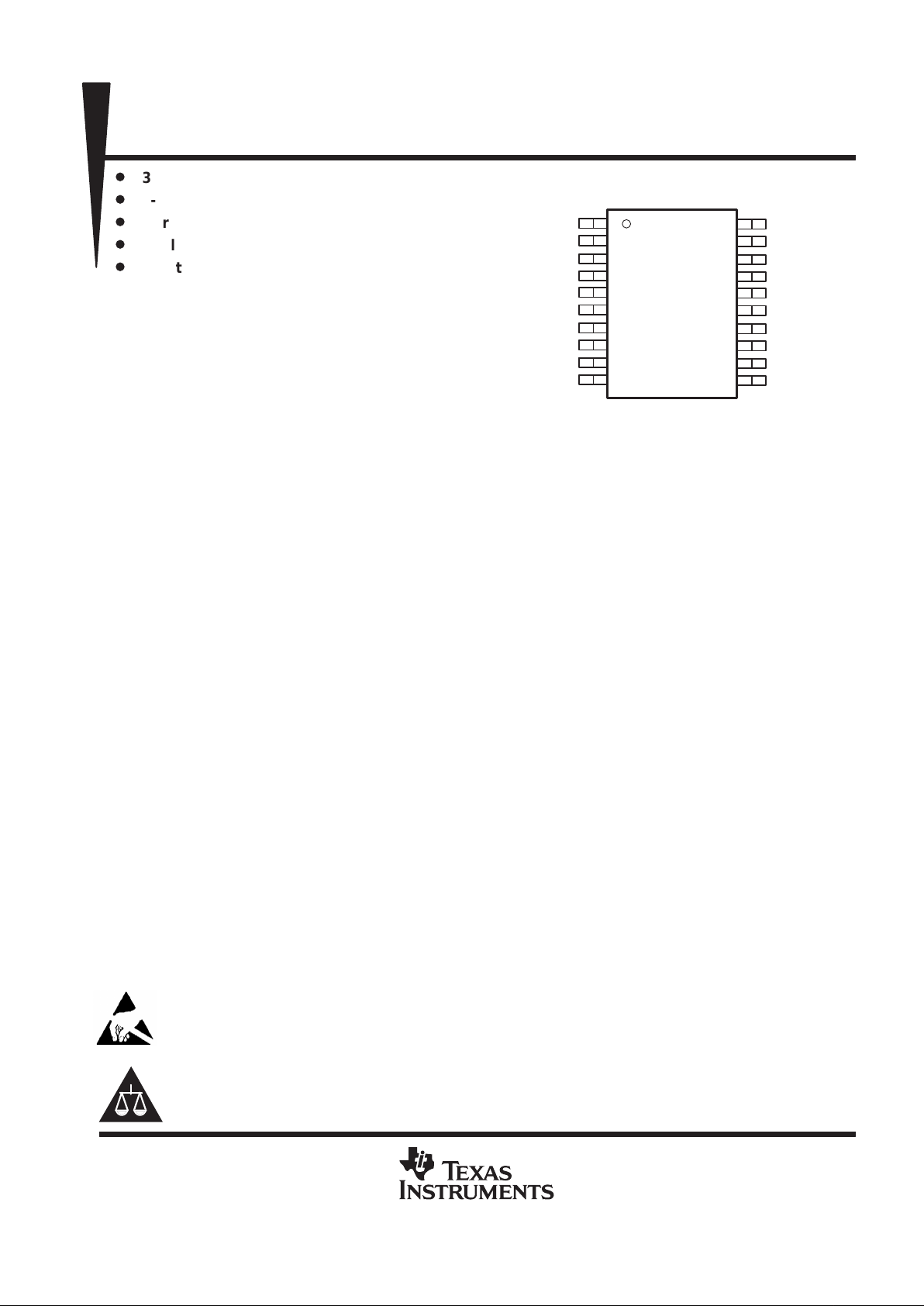
1
2
3
4
5
6
7
8
9
10
20
19
18
17
16
15
14
13
12
11
CLOCK
DATA
STROBE
VSS
RFINP
RFINN
VCCP
REFIN
RA
AUXIN
VDD
NENM
LOCK
NENA
RN
VDDA
PHP
PHI
VSSA
PHA
PW PACKAGE
(TOP VIEW)

TRF2052
LOW-VOLTAGE 2-GHz SYNTHESIZER
SLWS066 – JULY 1998
2
POST OFFICE BOX 655303 • DALLAS, TEXAS 75265
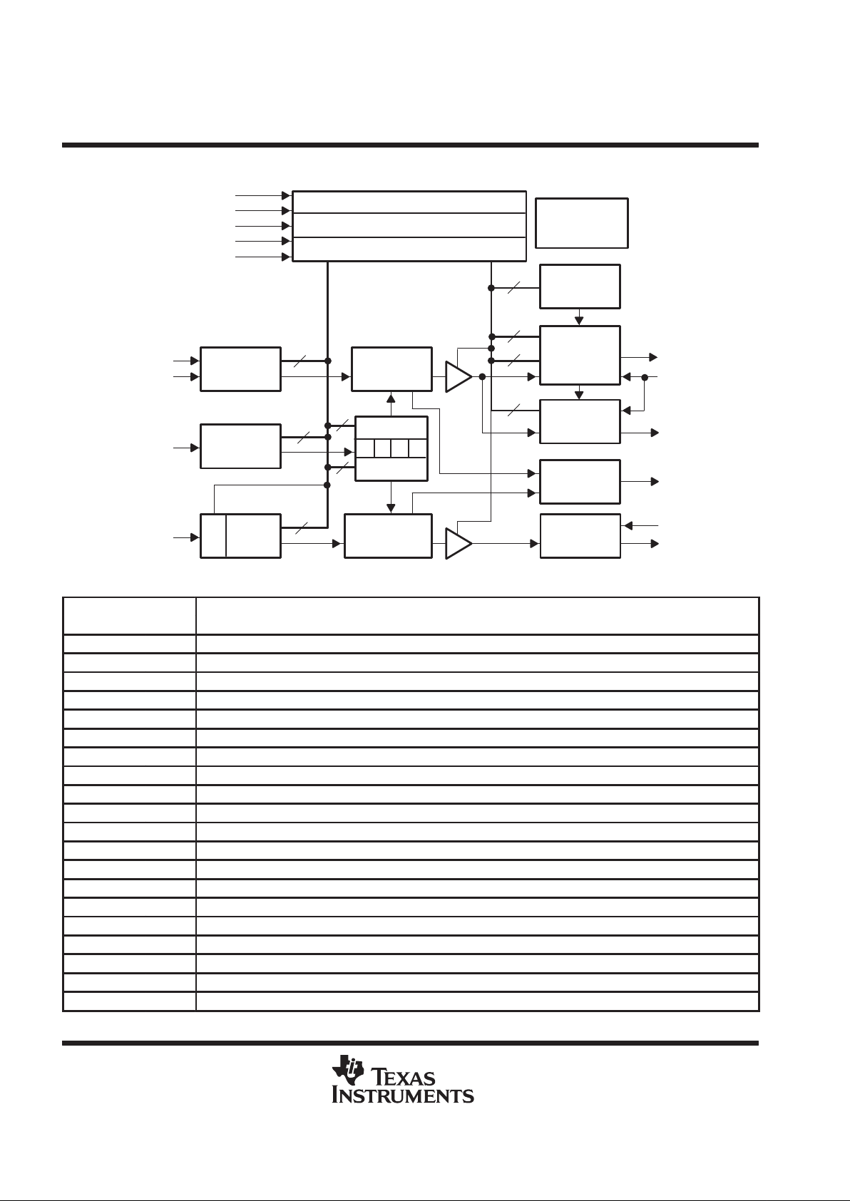
functional block diagram
Serial Control Shift Register
Control and Selection
Internal Control Register
Band Gap
and Bias
DATA
CLOCK
STROBE
NENM
NENA
Main Divider
N
Main Phase
Detector
MCP
1/–1
Speed-Up
Counter
G
Main
Charge Pump
CN
CL
Intergral
Charge Pump
CK
SELECT
SELECT
1 2 4 8
Reference
Divider
M
SM
2 Lock
Detector
Auxiliary
Divider
NA
Auxiliary
Phase Detector
ACP
1/–1
4/1
PA
Auxiliary
Charge Pump
PHP
RN
PHI
LOCK
RA
PHA
RFINP
RFINN
REFIN
AUXIN
2
1
3
19
17
3
5
6
8
10
14
16
13
18
9
11
18
12
12
8
8
2
4
SA
2
Terminal Functions
TERMINAL
NAME NO.
DESCRIPTION
AUXIN 10 Auxiliary channel RF input
CLOCK 1 Serial interface clock signal
DATA 2 Serial interface data signal
LOCK 18 Lock detector output
NENA 17 Enable signal for the auxiliary channel/main channel/open loop. See modes of operation logic table. Active low
NENM 19 Enable signal for the auxiliary channel/main channel/open loop. See modes of operation logic table. Active low
PHA 11 Auxiliary charge pump output
PHI 13 Integral charge pump output
PHP 14 Main (proportional) charge pump output
RA 9 Resistor to VSSA sets auxiliary charge pump current
REFIN 8 Reference frequency input signal
RFINN 6 Prescaler negative RF input
RFINP 5 Prescaler positive RF input
RN 16 Resistor to VSSA sets main charge pump current
STROBE 3 Serial interface load signal
VCCP 7 Prescaler positive supply voltage
VDD 20 Digital supply voltage
VDDA 15 Analog supply voltage
VSS 4 Digital/prescaler ground
VSSA 12 Analog ground

TRF2052
LOW-VOLTAGE 2-GHz SYNTHESIZER
SLWS066 – JULY 1998
3
POST OFFICE BOX 655303 • DALLAS, TEXAS 75265
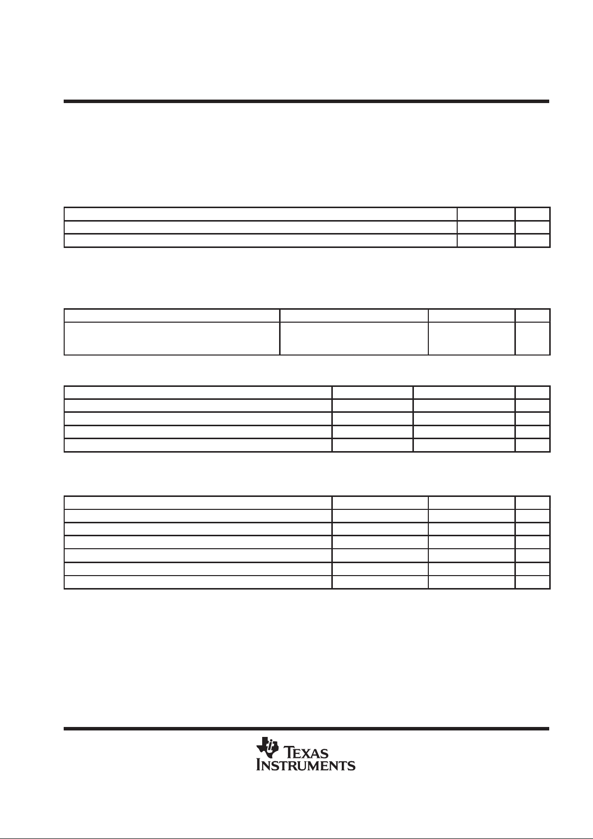
absolute maximum ratings over operating free-air temperature (unless otherwise noted)
Supply voltage range (See Note 1) –0.6 to 4.7 Vdc. . . . . . . . . . . . . . . . . . . . . . . . . . . . . . . . . . . . . . . . . . . . . . . . .
Input voltage, logic signals –0.6 to 4.7 Vdc. . . . . . . . . . . . . . . . . . . . . . . . . . . . . . . . . . . . . . . . . . . . . . . . . . . . . . . .
Storage temperature range –65°C to 150°C. . . . . . . . . . . . . . . . . . . . . . . . . . . . . . . . . . . . . . . . . . . . . . . . . . . . . . . .
ESD protection, all pins, human body model 1 kV. . . . . . . . . . . . . . . . . . . . . . . . . . . . . . . . . . . . . . . . . . . . . . . . . . .
NOTE 1: Voltage values are with respect to VSSA.
recommended operating conditions
MIN MAX UNIT
Supply voltage, VCCP, VDD, VDDA 2.7 3.3 V
Operating free-air temperature, T
A
–10 55 °C
dc electrical characteristics over full range of operating conditions,
typical values are at VCCP = VDD = VDDA = 3 V, T
A
= 25°C (unless otherwise noted)
supply current
PARAMETER TEST CONDITIONS MIN TYP MAX UNIT
Average operational supply current (see Note 2)
EM = EA = 1
|I
PHA
| = 1 mA
|I
PHP S
| = 2.5 mA
ES = 0
|I
PHP N
| = 0.5 mA
|
IPHI
| = 0 mA
11.4 mA
NOTE 2: Charge pump output current not included.
digital interface
PARAMETER TEST CONDITIONS MIN TYP MAX UNIT
V
OH
High-level output voltage (LOCK) IOH = 1 mA VCC – 0.5 V
V
OL
Low-level output voltage (LOCK) IOL = –1 mA 0.5 V
V
IH
High-level input voltage (DATA, CLOCK, STROBE, NENA, NENM) IIH = 10 µA VCC – 0.5 V
V
IL
Low-level input voltage (DATA, CLOCK, STROBE, NENA, NENM) IIL = 10 µA 0.5 V
ac electrical characteristics over full range of operating conditions,
typical values are at VCCP = VDD = VDDA = 3 V, T
A
= 25°C (unless otherwise noted)
PARAMETER TEST CONDITIONS MIN TYP MAX UNIT
RF input frequency 0.1 2.0 GHz
Differential RF input voltage –16 –3 dBm
Reference input frequency 13.8 MHz
Reference input voltage 0.3 V
pp
Auxiliary input frequency (see Note 3) 150 MHz
Auxiliary input voltage 0.2 V
pp
NOTE 3: Used with predivider (1/4)
 Loading...