

TRF2052
LOW-VOLTAGE 2-GHz SYNTHESIZER
SLWS066 – JULY 1998
1
POST OFFICE BOX 655303 • DALLAS, TEXAS 75265
D
3-V Power Supply Operation
D
2-GHz Operation
D
Normal and Speed-Up Charge Pumps
D
Dual PLL: One RF and One IF
D
Additional, Directly Accessible
Power-Down Modes
description
The TRF2052 is a dual-channel, low-power,
phase-locked loop (PLL) frequency synthesizer
component designed specifically for digitally enhanced cordless telephone (DECT) applications.
The device is suitable for a variety of applications
up through 2 GHz. A speed-up integral charge pump is used for fast channel switching. The simple serial
interface is compatible with the extended performance mode (EPM) of other devices in Texas Instruments’
synthesizer family.
Along with the external loop filters, the TRF2052 provides all functions for voltage-controlled oscillators (VCO)
in a dual-PLL frequency synthesizer system. A main channel is provided for RF frequencies and an auxiliary
channel for IF frequencies. The current-output charge pumps directly drive passive RC filter networks, to
generate VCO control voltages. Fast main-channel frequency switching is achieved with a charge pump
arrangement that increases the current drive and alters the loop-filter frequency response during a portion of
the switching interval.
The speed-up mode is controlled by the serial interface strobe signal, which goes high when a new frequency
is loaded. At this time, the internal speed-up timer is activated and it enables the speed-up mode into the
speed-up timer for the preprogrammed duration. During speed-up mode, the charge pump current to the
external loop filter can be changed in two ways. First, the main charge pump current can be increased. Second,
an additional integral charge pump can be separately and directly connected to the external loop-filter capacitor
to further decrease the loop-filter charge and discharge times.
Caution. These devices have limited built-in gate protection. The leads should be shorted together or the device placed in conductive
foam during storage or handling to prevent electrostatic damage to the MOS gates.
Please be aware that an important notice concerning availability, standard warranty, and use in critical applications of
Texas Instruments semiconductor products and disclaimers thereto appears at the end of this data sheet.
Copyright 1998, Texas Instruments Incorporated
PRODUCTION DATA information is current as of publication date.
Products conform to specifications per the terms of Texas Instruments
standard warranty. Production processing does not necessarily include
testing of all parameters.
1
2
3
4
5
6
7
8
9
10
20
19
18
17
16
15
14
13
12
11
CLOCK
DATA
STROBE
VSS
RFINP
RFINN
VCCP
REFIN
RA
AUXIN
VDD
NENM
LOCK
NENA
RN
VDDA
PHP
PHI
VSSA
PHA
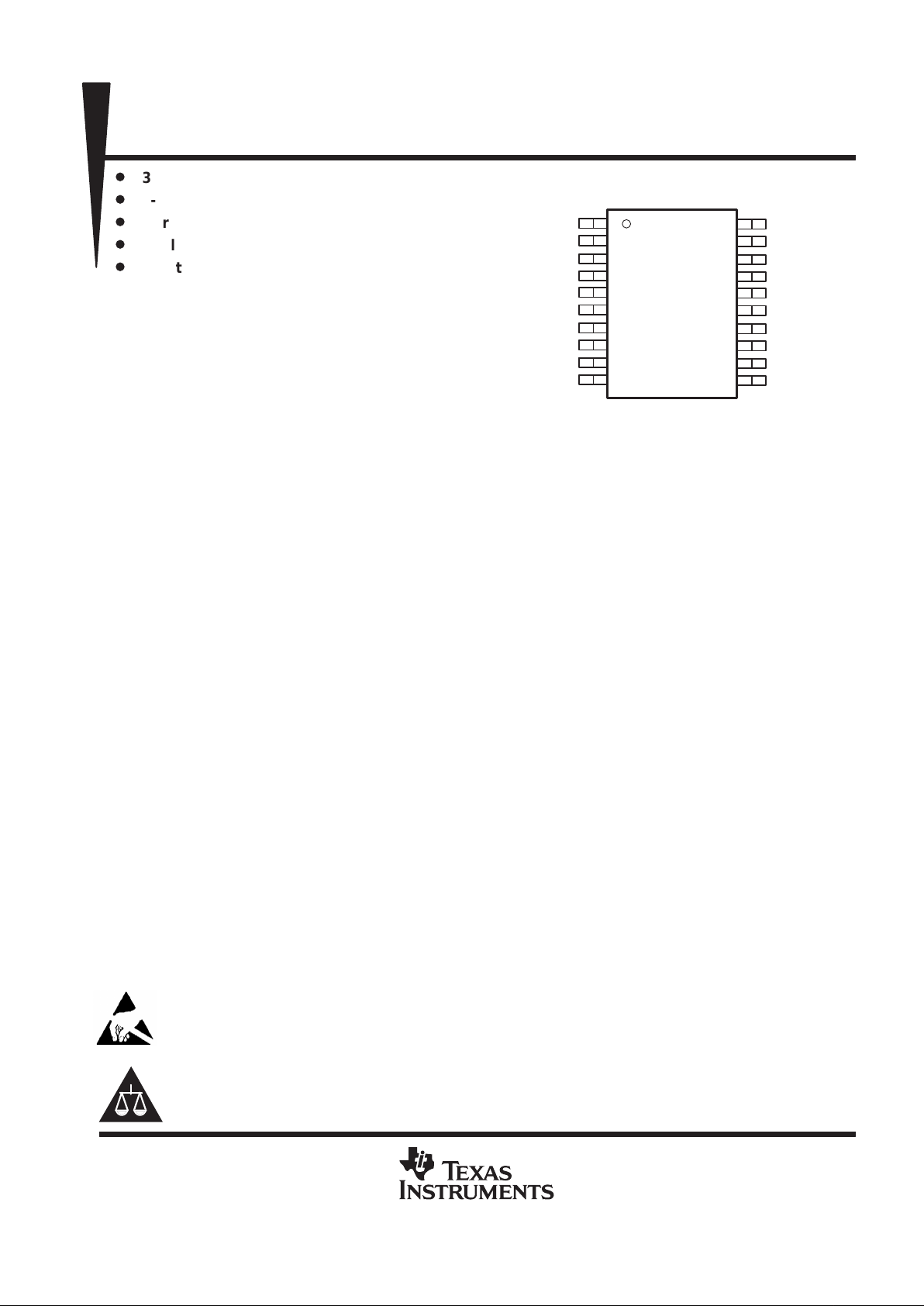
PW PACKAGE
(TOP VIEW)
TRF2052
LOW-VOLTAGE 2-GHz SYNTHESIZER
SLWS066 – JULY 1998
2
POST OFFICE BOX 655303 • DALLAS, TEXAS 75265
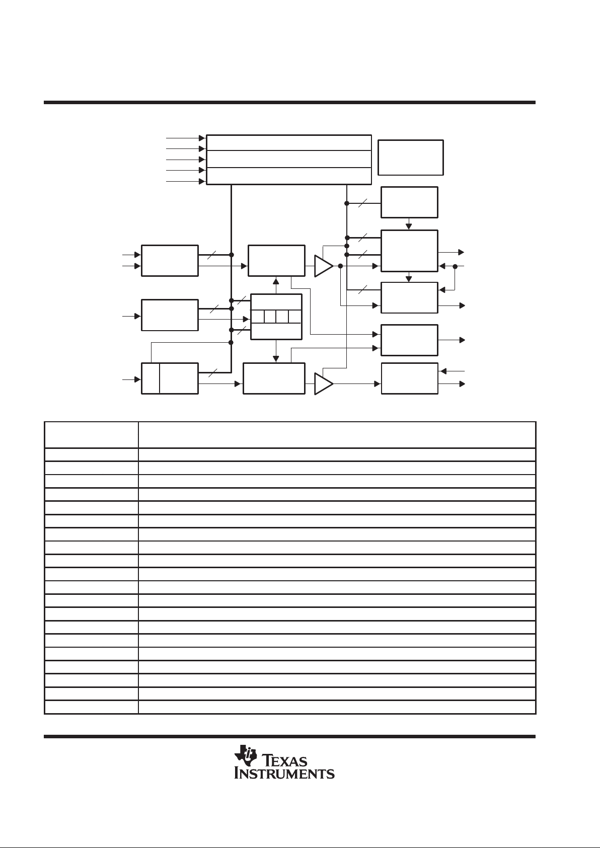
functional block diagram
Serial Control Shift Register
Control and Selection
Internal Control Register
Band Gap
and Bias
DATA
CLOCK
STROBE
NENM
NENA
Main Divider
N
Main Phase
Detector
MCP
1/–1
Speed-Up
Counter
G
Main
Charge Pump
CN
CL
Intergral
Charge Pump
CK
SELECT
SELECT
1 2 4 8
Reference
Divider
M
SM
2 Lock
Detector
Auxiliary
Divider
NA
Auxiliary
Phase Detector
ACP
1/–1
4/1
PA
Auxiliary
Charge Pump
PHP
RN
PHI
LOCK
RA
PHA
RFINP
RFINN
REFIN
AUXIN
2
1
3
19
17
3
5
6
8
10
14
16
13
18
9
11
18
12
12
8
8
2
4
SA
2
Terminal Functions
TERMINAL
NAME NO.
DESCRIPTION
AUXIN 10 Auxiliary channel RF input
CLOCK 1 Serial interface clock signal
DATA 2 Serial interface data signal
LOCK 18 Lock detector output
NENA 17 Enable signal for the auxiliary channel/main channel/open loop. See modes of operation logic table. Active low
NENM 19 Enable signal for the auxiliary channel/main channel/open loop. See modes of operation logic table. Active low
PHA 11 Auxiliary charge pump output
PHI 13 Integral charge pump output
PHP 14 Main (proportional) charge pump output
RA 9 Resistor to VSSA sets auxiliary charge pump current
REFIN 8 Reference frequency input signal
RFINN 6 Prescaler negative RF input
RFINP 5 Prescaler positive RF input
RN 16 Resistor to VSSA sets main charge pump current
STROBE 3 Serial interface load signal
VCCP 7 Prescaler positive supply voltage
VDD 20 Digital supply voltage
VDDA 15 Analog supply voltage
VSS 4 Digital/prescaler ground
VSSA 12 Analog ground
TRF2052
LOW-VOLTAGE 2-GHz SYNTHESIZER
SLWS066 – JULY 1998
3
POST OFFICE BOX 655303 • DALLAS, TEXAS 75265
absolute maximum ratings over operating free-air temperature (unless otherwise noted)
Supply voltage range (See Note 1) –0.6 to 4.7 Vdc. . . . . . . . . . . . . . . . . . . . . . . . . . . . . . . . . . . . . . . . . . . . . . . . .
Input voltage, logic signals –0.6 to 4.7 Vdc. . . . . . . . . . . . . . . . . . . . . . . . . . . . . . . . . . . . . . . . . . . . . . . . . . . . . . . .
Storage temperature range –65°C to 150°C. . . . . . . . . . . . . . . . . . . . . . . . . . . . . . . . . . . . . . . . . . . . . . . . . . . . . . . .
ESD protection, all pins, human body model 1 kV. . . . . . . . . . . . . . . . . . . . . . . . . . . . . . . . . . . . . . . . . . . . . . . . . . .
NOTE 1: Voltage values are with respect to VSSA.
recommended operating conditions
MIN MAX UNIT
Supply voltage, VCCP, VDD, VDDA 2.7 3.3 V
Operating free-air temperature, T
A
–10 55 °C
dc electrical characteristics over full range of operating conditions,
typical values are at VCCP = VDD = VDDA = 3 V, T
A
= 25°C (unless otherwise noted)
supply current
PARAMETER TEST CONDITIONS MIN TYP MAX UNIT
Average operational supply current (see Note 2)
EM = EA = 1
|I
PHA
| = 1 mA
|I
PHP S
| = 2.5 mA
ES = 0
|I
PHP N
| = 0.5 mA
|
IPHI
| = 0 mA
11.4 mA
NOTE 2: Charge pump output current not included.
digital interface
PARAMETER TEST CONDITIONS MIN TYP MAX UNIT
V
OH
High-level output voltage (LOCK) IOH = 1 mA VCC – 0.5 V
V
OL
Low-level output voltage (LOCK) IOL = –1 mA 0.5 V
V
IH
High-level input voltage (DATA, CLOCK, STROBE, NENA, NENM) IIH = 10 µA VCC – 0.5 V
V
IL
Low-level input voltage (DATA, CLOCK, STROBE, NENA, NENM) IIL = 10 µA 0.5 V
ac electrical characteristics over full range of operating conditions,
typical values are at VCCP = VDD = VDDA = 3 V, T
A
= 25°C (unless otherwise noted)
PARAMETER TEST CONDITIONS MIN TYP MAX UNIT
RF input frequency 0.1 2.0 GHz
Differential RF input voltage –16 –3 dBm
Reference input frequency 13.8 MHz
Reference input voltage 0.3 V
pp
Auxiliary input frequency (see Note 3) 150 MHz
Auxiliary input voltage 0.2 V
pp
NOTE 3: Used with predivider (1/4)

TRF2052
LOW-VOLTAGE 2-GHz SYNTHESIZER
SLWS066 – JULY 1998
4
POST OFFICE BOX 655303 • DALLAS, TEXAS 75265
charge pump output currents
The steepness of the phase detector charge-pump chains is determined by external resistors between the
dedicated pins RA and RN and ground, as well as by user programmable variables. The charts that follow
indicate how the charge-pump peak currents can be set by the external resistors and the control variables.
auxiliary charge pump
PARAMETER TEST CONDITIONS MIN TYP MAX UNIT
|I
PHA
| Open loop mode (NENA = 1) 0 vV
PHA
vV
DDA
10 pA
|I
PHA
| Closed loop mode (NENA = 0)
0.5 V vV
PHA
vV
DDA
– 0.5 V,
RA w = 18 kΩ
20 × 1.25/RA[kΩ] mA
main charge pump
PARAMETER TEST CONDITIONS MIN TYP MAX UNIT
|I
PHM_N
| Normal mode
0.5 V vV
PHP
vV
DDA
– 0.5 V,
18.75/(RN[kΩ] + 0.75) ×
CN/256
mA
|I
PHM_S
| Speed-up mode (see Note 4)
R
N
w = 18
kΩ
|I
PHM_N
| × (1 + 2CL + 1) mA
4. The maximum allowable current is 12 mA. It is recommended to use the speedup mode only before the PLL is locked. Switching
between speedup and normal modes as well as changing the current setting factor CN, under PLL operation, may cause
disturbances in the VCO control voltage.
integral charge pump
PARAMETER TEST CONDITIONS MIN TYP MAX UNIT
|I
PHI_N
| Normal mode 0 vV
PHI
vV
DDA
0 mA
|I
PHI_S
| Speed-up mode (see Note 5)
0.5 V vV
PHI
vV
DDA
– 0.5 V,
RN w = 18 kΩ,
|I
PHM_S
| v 16 mA
|I
PHM_N
| × 2CL + 1 × CK mA
5. Maximum allowable current is 24 mA
The instantaneous values of the charge pump currents are related to the phase error by:
I
PH_inst
+
Q
error
2
p
I
PH_peak
modes of operation
†
CHIP MODE NENM NENA ACTIVE STAGES
Both synthesizers on 0 0 Everything on
Main synthesizers on 0 1 Only auxiliary charge pump set to triple state; everything else working
Auxiliary synthesizer on 1 0 Main loop disabled, auxiliary loop working
Shutdown 1 1 All off
†
Enable signals, NENM and NENA, are active low.
timing requirements, serial data interface (see Figure 1)
PARAMETER MIN MAX UNIT
f
(CLOCK)
Clock frequency 10 MHz
t
w(CLKHI)
Clock high-time pulse width, Clock high 30 ns
t
w(CLKLO)
Clock low-time pulse width, Clock low 30 ns
t
su(D)
Set-up time, data valid before CLOCK↑ 30 ns
t
h(D)
Hold time, data valid after CLOCK↑ 30 ns
t
su(STROBE)
Set-up time, STROBE↑ before CLOCK↑ 30 ns
t
w(STROBEHI)
STROBE high-time pulse width, STROBE high 30 ns
t
w(STROBELO)
STROBE low-time pulse width, STROBE low 30 ns
(1)

TRF2052
LOW-VOLTAGE 2-GHz SYNTHESIZER
SLWS066 – JULY 1998
5
POST OFFICE BOX 655303 • DALLAS, TEXAS 75265
P ARAMETER MEASUREMENT INFORMATION
t
su(STROBE)
t
su(D)
t
h(D)
DATA
CLOCK
STROBE
t
w(CLKH)
t
w(STROBEHI)
t
w(STROBELO)
f(CLOCK)
t
w(CLKLO)
Figure 1. Serial-Data Interface Timing

TRF2052
LOW-VOLTAGE 2-GHz SYNTHESIZER
SLWS066 – JULY 1998
6
POST OFFICE BOX 655303 • DALLAS, TEXAS 75265
PRINCIPLES OF OPERATION
serial control
The TRF2052 internal registers contain all the user programmable variables such as divider ratios, charge pump
settings, etc. They are programmed using a three-wire (CLOCK, DATA, STROBE) serial interface.
At every rising slope of the CLOCK signal, the actual logical value on the DA TA pin is written into a 24-bit shift
register. A rising slope on the STROBE pin causes the actual content of the shift register to be input as a control
word.
The control word is, therefore, 24-bits long and the first incoming bit functions as the least significant bit (LSB),
bit 0. If the most significant bit (MSB), bit 23, is 1, the word functions as control word A. If the MSB is 0, bits 20
to 22 become address bits, which label the words as control word B through E, respectively . To fully program
the synthesizer, four words must be sent: A, B, C, and D. Word E is for test purposes only.
The position of the individual variables within the control words is illustrated in Figure 2. T able 1 briefly describes
their functions. The G parameter, which specifies the duration of the speed-up mode in reference divider cycles,
splits into most significant (G2) and least significant (G1) nibbles.
0G1 N
1 0 0 0 CN CK CL
M
C
P
1001 NA
1 0 1 0 NR SM SA
1111
MSB
Last In
LSB
First In
A
B
C
D
E
E
M
E
A
TST<10:0>
23 22 21 20 1918 17 16 15 14 13 12 11 10 9 8 7 6 5 4 3 2 1 0
nc
G2
A
C
P
P
A
nc
ESP
M
nc
Figure 2. Serial Word Format

TRF2052
LOW-VOLTAGE 2-GHz SYNTHESIZER
SLWS066 – JULY 1998
7
POST OFFICE BOX 655303 • DALLAS, TEXAS 75265
PRINCIPLES OF OPERATION
Table 1. Function Table
SYMBOL BITS FUNCTION
N 18 Overall main divider integer division ratio
CN 8 Binary current setting factor for main charge pumps
G2 4 MS bits for the speed-up mode duration (number of reference divider cycles)
G1 4 LS bits for the speed-up mode duration (number of reference divider cycles)
CK 4 Binary acceleration factor for integral charge pump current
CL 2 Binary acceleration factor for increase in main charge pump current during speed-up mode
MCP 1 Main charge pump polarity
ACP 1 Auxiliary charge pump polarity
NA 12 Auxiliary divider ratio
PA 1 Auxiliary prescaler select:
0 = divide by 4
1 = divide by 1
NR 12 Reference divider ratio
SM 2 Reference select for main phase detector
EM 1 Main divider enable flag
SA 2 Reference select for auxiliary phase detector
EA 1 Auxiliary divider enable flag
ES 1 Speed-up mode standby control:
0 = speed-up charge pump switches off completely if no fast mode
1 = speed-up charge pump always in standby
PM 1 Phase detector mode. Change between two modes for reset pulse generation:
0 = analog internal generated delay
1 = high-pulse duration for REF-CLOCK
RF inputs
The differential main divider input has a resistance of several kW and can be matched to the system impedance
by an external resistor. To form a single ended input, any one of the input pins can be grounded by a blocking
capacitor.
The auxiliary channel RF and reference inputs have a high resistance, as well, and are single ended. If needed,
matching can be accomplished with an external resistor.
enabling the PLLs
Both PLLs can be enabled and disabled independently , either by the serial control variables EM and EA or by
the digital inputs pins NENM and NENA.
The serial control variables and the hardware signal NENM disable the charge pump and the divider of the
corresponding loop, while NENA affects the auxiliary charge pump output only . This helps to avoid spikes that
might occur after re–enabling the auxiliary loop by the serial interface.

TRF2052
LOW-VOLTAGE 2-GHz SYNTHESIZER
SLWS066 – JULY 1998
8
POST OFFICE BOX 655303 • DALLAS, TEXAS 75265
MECHANICAL DATA
PW (R-PDSO-G**) PLASTIC SMALL-OUTLINE PACKAGE
4040064/E 08/96
14 PIN SHOWN
Seating Plane
0,05 MIN
1,20 MAX
1
A
7
14
0,19
4,50
4,30
8
6,20
6,60
0,30
0,75
0,50
0,25
Gage Plane
0,15 NOM
0,65
M
0,10
0°–8°
0,10
PINS **
A MIN
A MAX
DIM
2,90
3,10
8
4,90
5,10
14
6,60
6,404,90
5,10
16
7,70
20
7,90
24
9,60
9,80
28
NOTES: A. All linear dimensions are in millimeters.
B. This drawing is subject to change without notice.
C. Body dimensions do not include mold flash or protrusion not to exceed 0,15.
D. Falls within JEDEC MO-153

IMPORTANT NOTICE
T exas Instruments and its subsidiaries (TI) reserve the right to make changes to their products or to discontinue
any product or service without notice, and advise customers to obtain the latest version of relevant information
to verify, before placing orders, that information being relied on is current and complete. All products are sold
subject to the terms and conditions of sale supplied at the time of order acknowledgement, including those
pertaining to warranty, patent infringement, and limitation of liability.
TI warrants performance of its semiconductor products to the specifications applicable at the time of sale in
accordance with TI’s standard warranty. Testing and other quality control techniques are utilized to the extent
TI deems necessary to support this warranty. Specific testing of all parameters of each device is not necessarily
performed, except those mandated by government requirements.
CERT AIN APPLICATIONS USING SEMICONDUCTOR PRODUCTS MAY INVOLVE POTENTIAL RISKS OF
DEATH, PERSONAL INJURY, OR SEVERE PROPERTY OR ENVIRONMENTAL DAMAGE (“CRITICAL
APPLICATIONS”). TI SEMICONDUCTOR PRODUCTS ARE NOT DESIGNED, AUTHORIZED, OR
WARRANTED TO BE SUITABLE FOR USE IN LIFE-SUPPORT DEVICES OR SYSTEMS OR OTHER
CRITICAL APPLICATIONS. INCLUSION OF TI PRODUCTS IN SUCH APPLICA TIONS IS UNDERST OOD TO
BE FULLY AT THE CUSTOMER’S RISK.
In order to minimize risks associated with the customer’s applications, adequate design and operating
safeguards must be provided by the customer to minimize inherent or procedural hazards.
TI assumes no liability for applications assistance or customer product design. TI does not warrant or represent
that any license, either express or implied, is granted under any patent right, copyright, mask work right, or other
intellectual property right of TI covering or relating to any combination, machine, or process in which such
semiconductor products or services might be or are used. TI’s publication of information regarding any third
party’s products or services does not constitute TI’s approval, warranty or endorsement thereof.
Copyright 1998, Texas Instruments Incorporated
 Loading...