

Texas Instruments TPS76933DBVR, TPS76930DBVT, TPS76930DBVR, TPS76928DBVT, TPS76928DBVR Datasheet
...
TPS76901, TPS76912, TPS76915, TPS76918, TPS76925
TPS76927, TPS76928, TPS76930, TPS76933, TPS76950
ULTRALOW-POWER 100-mA LOW-DROPOUT LINEAR REGULATORS
SLVS203D – JUNE 1999 – REVISED APRIL 2000
1
POST OFFICE BOX 655303 • DALLAS, TEXAS 75265
D
100-mA Low-Dropout Regulator
D
Available in 1.2-V, 1.5-V, 1.8-V, 2.5-V, 2.7-V,
2.8-V, 3.0-V, 3.3-V, and 5-V Fixed-Output and
Adjustable Versions
D
Only 17 µA Quiescent Current at 100 mA
D
1 µA Quiescent Current in Standby Mode
D
Dropout Voltage Typically 71 mV at 100mA
D
Over Current Limitation
D
–40°C to 125°C Operating Junction
T emperature Range
D
5-Pin SOT-23 (DBV) Package
description
The TPS769xx family of low-dropout (LDO)
voltage regulators offers the benefits of low
dropout voltage, ultralow-power operation, and
miniaturized packaging. These regulators feature
low dropout voltages and ultralow quiescent
current compared to conventional LDO
regulators. Offered in a 5-terminal small outline
integrated-circuit SOT-23 package, the
TPS769xx series devices are ideal for
micropower operations and where board space is
at a premium.
A combination of new circuit design and process
innovation has enabled the usual PNP pass
transistor to be replaced by a PMOS pass
element. Because the PMOS pass element
behaves as a low-value resistor, the dropout
voltage is very low, typically 71 mV at 100 mA of
load current (TPS76950), and is directly proportional to the load current. Since the PMOS pass element is a
voltage-driven device, the quiescent current is ultralow (28 µA maximum) and is stable over the entire range
of output load current (0 mA to 100 mA). Intended for use in portable systems such as laptops and cellular
phones, the ultralow-dropout voltage feature and ultralow-power operation result in a significant increase in
system battery operating life.
The TPS769xx also features a logic-enabled sleep mode to shut down the regulator, reducing quiescent current
to 1 µA typical at T
J
= 25°C. The TPS769xx is offered in 1.2-V, 1.5-V, 1.8-V, 2.5-V, 2.7-V, 2.8-V, 3.0-V, 3.3-V,
and 5-V fixed-voltage versions and in a variable version (programmable over the range of 1.2 V to 5.5 V).
Copyright 2000, Texas Instruments Incorporated
PRODUCTION DATA information is current as of publication date.
Products conform to specifications per the terms of Texas Instruments
standard warranty. Production processing does not necessarily include
testing of all parameters.
Please be aware that an important notice concerning availability, standard warranty, and use in critical applications of
Texas Instruments semiconductor products and disclaimers thereto appears at the end of this data sheet.
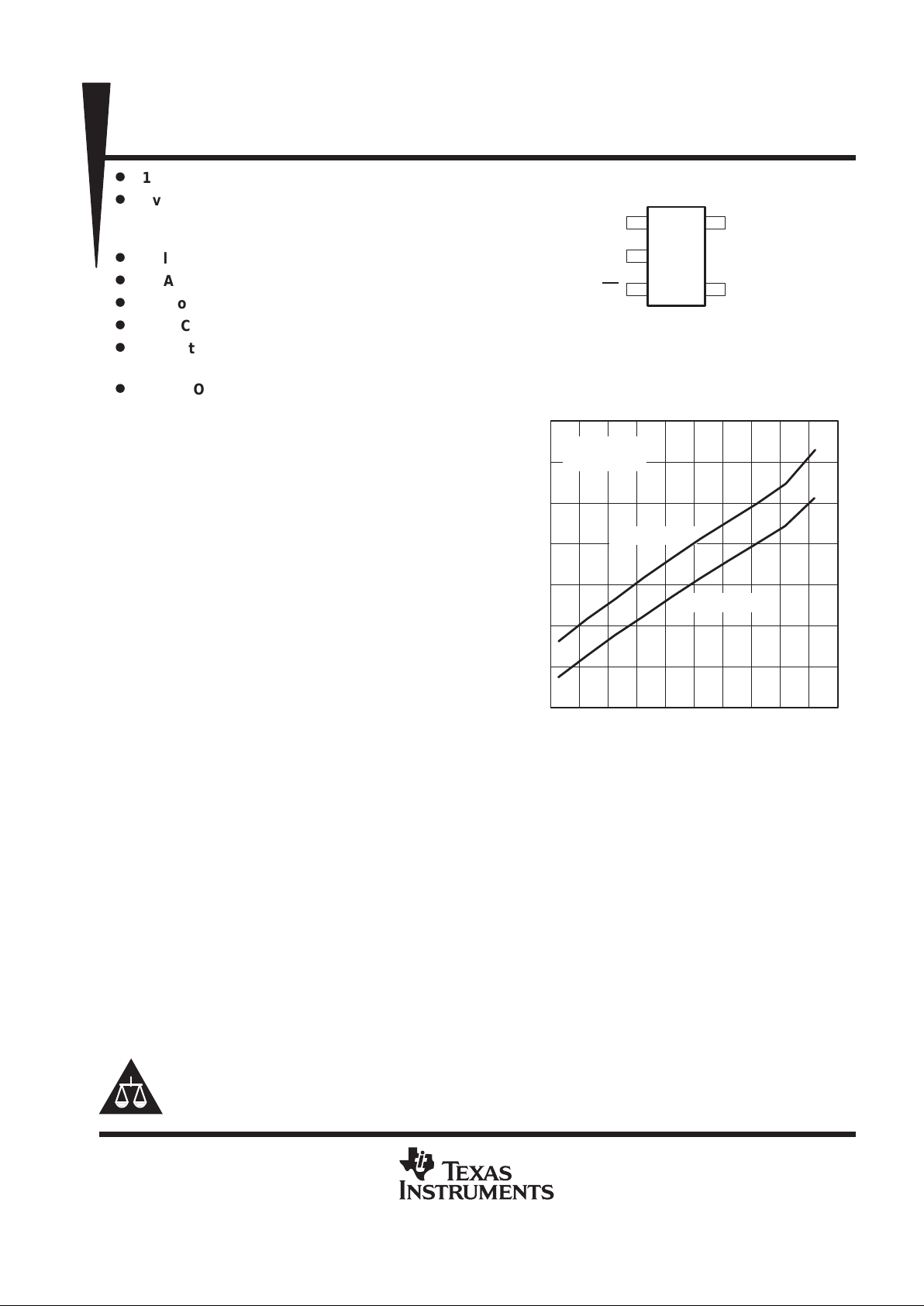
3
2
4
5
DBV PACKAGE
(TOP VIEW)
1
IN
GND
EN
OUT
NC/FB
TA – Free-Air Temperature – °C
15
22
TPS76933
GROUND CURRENT
vs
FREE-AIR TEMPERATURE
Ground Current – Aµ
VI = 4.3 V
CO = 4.7 µF
–40 0–20 20 140–60 40 80 100 12060
21
20
19
18
17
16
IO = 0 mA
IO = 100 mA
TPS76901, TPS76912, TPS76915, TPS76918, TPS76925
TPS76927, TPS76928, TPS76930, TPS76933, TPS76950
ULTRALOW-POWER 100-mA LOW-DROPOUT LINEAR REGULATORS
SLVS203D – JUNE 1999 – REVISED APRIL 2000
2
POST OFFICE BOX 655303 • DALLAS, TEXAS 75265
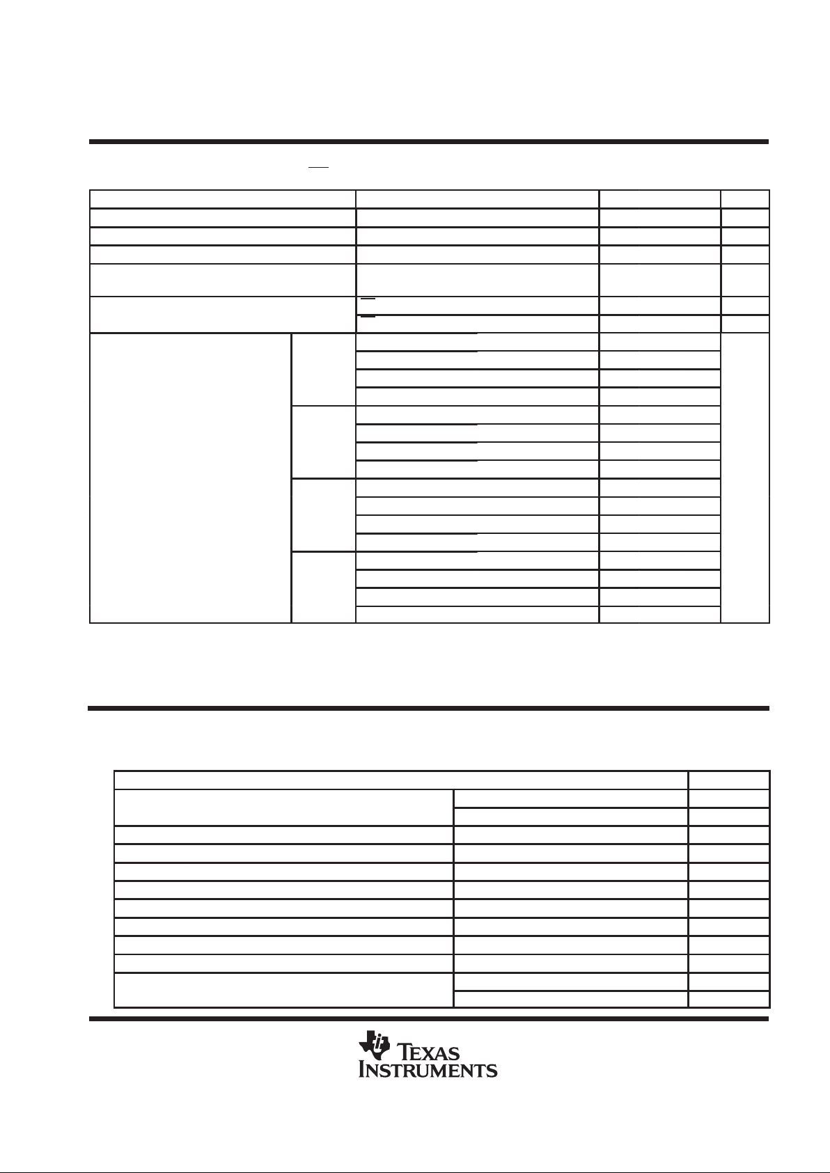
AVAILABLE OPTIONS
T
J
VOLTAGE PACKAGE PART NUMBER SYMBOL
Variable
1.2V to 5.5V
TPS76901DBVT†TPS76901DBVR
‡
PCFI
1.2 V TPS76912DBVT†TPS76912DBVR
‡
PCGI
1.5 V TPS76915DBVT†TPS76915DBVR
‡
PCHI
1.8 V
TPS76918DBVT†TPS76918DBVR
‡
PCII
–40°C to 125°C
2.5 V
SOT-23
TPS76925DBVT†TPS76925DBVR
‡
PCJI
2.7 V
(DBV)
TPS76927DBVT†TPS76927DBVR
‡
PCKI
2.8 V TPS76928DBVT†TPS76928DBVR
‡
PCLI
3.0 V TPS76930DBVT†TPS76930DBVR
‡
PCMI
3.3 V TPS76933DBVT†TPS76933DBVR
‡
PCNI
5.0 V TPS76950DBVT†TPS76950DBVR
‡
PCOI
†
The DBVT indicates tape and reel of 250 parts.
‡
The DBVR indicates tape and reel of 3000 parts.
functional block diagram
TPS76901
OUT
IN
FB
GND
EN
V
REF
TPS76912/15/18/25/27/28/30/33/50
OUT
IN
GND
EN
V
REF
Current Limit
/ Thermal
Protection
Current Limit
/ Thermal
Protection
TPS76901, TPS76912, TPS76915, TPS76918, TPS76925
TPS76927, TPS76928, TPS76930, TPS76933, TPS76950
ULTRALOW-POWER 100-mA LOW-DROPOUT LINEAR REGULATORS
SLVS203D – JUNE 1999 – REVISED APRIL 2000
3
POST OFFICE BOX 655303 • DALLAS, TEXAS 75265
Terminal Functions
TERMINAL
NAME NO.
I/O
DESCRIPTION
GND 2 Ground
EN 3 I Enable input
FB 4 I Feedback voltage (TPS76901 only)
IN 1 I Input supply voltage
NC 4 No connection (Fixed options only)
OUT 5 O Regulated output voltage
absolute maximum ratings over operating free-air temperature range (unless otherwise noted)
Ĕ
Input voltage range
(see Note 1)
–0.3 V to 13.5 V. . . . . . . . . . . . . . . . . . . . . . . . . . . . . . . . . . . . . . . . . . . . . . . . . .
Voltage range at EN –0.3 V to VI + 0.3 V. . . . . . . . . . . . . . . . . . . . . . . . . . . . . . . . . . . . . . . . . . . . . . . . . . . . . . . . . . .
Voltage on OUT, FB 7 V. . . . . . . . . . . . . . . . . . . . . . . . . . . . . . . . . . . . . . . . . . . . . . . . . . . . . . . . . . . . . . . . . . . . . . . . . .
Peak output current Internally limited. . . . . . . . . . . . . . . . . . . . . . . . . . . . . . . . . . . . . . . . . . . . . . . . . . . . . . . . . . . . . .
ESD rating, HBM 2 kV. . . . . . . . . . . . . . . . . . . . . . . . . . . . . . . . . . . . . . . . . . . . . . . . . . . . . . . . . . . . . . . . . . . . . . . . . .
Continuous total power dissipation See Dissipation Rating Table. . . . . . . . . . . . . . . . . . . . . . . . . . . . . . . . . . . . .
Operating virtual junction temperature range, T
J
–40°C to 150°C. . . . . . . . . . . . . . . . . . . . . . . . . . . . . . . . . . . . .
Storage temperature range, T
stg
–65°C to 150°C. . . . . . . . . . . . . . . . . . . . . . . . . . . . . . . . . . . . . . . . . . . . . . . . . . .
†
Stresses beyond those listed under “absolute maximum ratings” may cause permanent damage to the device. These are stress ratings only, and
functional operation of the device at these or any other conditions beyond those indicated under “recommended operating conditions” is not
implied. Exposure to absolute-maximum-rated conditions for extended periods may affect device reliability.
NOTE 1: All voltage values are with respect to network ground terminal.
DISSIPATION RATING TABLE
PACKAGE
TA ≤ 25°C
POWER RATING
DERATING FACTOR
ABOVE TA = 25°C
TA = 70°C
POWER RATING
TA = 85°C
POWER RATING
Recommended DBV 350 mW 3.5 mW/°C 192 mW 140 mW
Absolute Maximum DBV 437 mW 3.5 mW/°C 280 mW 227 mW
recommended operating conditions
MIN NOM MAX UNIT
Input voltage, VI (see Note 2) 2.7 10 V
Output voltage range, V
O
1.2 5.5 V
Continuous output current, IO (see Note 3) 0 100 mA
Operating junction temperature, T
J
–40 125 °C
NOTES: 2. To calculate the minimum input voltage for your maximum output current, use the following formula:
VI(min) = VO(max) + VDO (max load)
3. Continuous output current and operating junction temperature are limited by internal protection circuitry , but it is not recommended
that the device operate under conditions beyond those specified in this table for extended periods of time.
TPS76901, TPS76912, TPS76915, TPS76918, TPS76925
TPS76927, TPS76928, TPS76930, TPS76933, TPS76950
ULTRALOW-POWER 100-mA LOW-DROPOUT LINEAR REGULATORS
SLVS203D – JUNE 1999 – REVISED APRIL 2000
4
POST OFFICE BOX 655303 • DALLAS, TEXAS 75265
electrical characteristics over recommended operating free-air temperature range,
V
I
= V
O(typ)
+ 1 V, I
O
= 100 mA, EN = 0 V, C
O
= 4.7 µF (unless otherwise noted)
PARAMETER TEST CONDITIONS MIN TYP MAX UNIT
1.2 V ≤ VO ≤ 5.5 V, TJ = 25°C V
O
TPS76901
1.2 V ≤ VO ≤ 5.5 V, TJ = –40°C to 125°C 0.97V
O
1.03V
O
TJ = 25°C, 2.7 V < VIN < 10 V 1.224
TPS76912
TJ = –40°C to 125°C, 2.7 V < VIN < 10 V 1.187 1.261
TJ = 25°C, 2.7 V < VIN < 10 V 1.5
TPS76915
TJ = –40°C to 125°C, 2.7 V < VIN < 10 V 1.455 1.545
TJ = 25°C, 2.8 V < VIN < 10 V 1.8
TPS76918
TJ = –40°C to 125°C, 2.8 V < VIN < 10 V 1.746 1.854
TJ = 25°C, 3.5 V < VIN < 10 V 2.5
Output voltage (10 µA to 100 mA
TPS76925
TJ = –40°C to 125°C, 3.5 V < VIN < 10 V 2.425 2.575
g( µ
load) (see Note 4)
TJ = 25°C, 3.7 V < VIN < 10 V 2.7
V
TPS76927
TJ = –40°C to 125°C, 3.7 V < VIN < 10 V 2.619 2.781
TJ = 25°C, 3.8 V < VIN < 10 V 2.8
TPS76928
TJ = –40°C to 125°C, 3.8 V < VIN < 10 V 2.716 2.884
TJ = 25°C, 4.0 V < VIN < 10 V 3.0
TPS76930
TJ = –40°C to 125°C, 4.0 V < VIN < 10 V 2.910 3.090
TJ = 25°C, 4.3 V < VIN < 10 V 3.3
TPS76933
TJ = –40°C to 125°C, 4.3 V < VIN < 10 V 3.201 3.399
TJ = 25°C, 6.0 V < VIN < 10 V 5.0
TPS76950
TJ = –40°C to 125°C, 6.0 V < VIN < 10 V 4.850 5.150
Quiescent current (GND current)
EN = 0V, 0 mA < IO < 100 mA,
TJ = 25°C
17
()
(See Note 4 and Note 5)
EN = 0V, IO = 100 mA,
TJ = –40°C to 125°C
28
µ
A
Load regulation
EN = 0V, IO = 0 to 100 mA,
TJ = 25°C
12 mV
p
VO + 1 V < VI ≤ 10 V, TJ = 25°C,
See Note 4
0.04
Output voltage line regulation (∆VO/VO) (See Note 5)
VO + 1 V < VI ≤ 10 V,
TJ = –40°C to 125°C, See Note 4
0.1
%/V
Output noise voltage
BW = 300 Hz to 50 kHz,
CO = 10 µF, TJ = 25°C
190 µVrms
Output current limit VO = 0 V, See Note 4 350 750 mA
EN = VI, 2.7 < VI < 10 V 1 µA
Standby current
TJ = –40°C to 125°C 2 µA
NOTES: 4. Minimum IN operating voltage is 2.7 V or V
O(typ)
+ 1 V , whichever is greater. Maximum IN voltage 10 V, minimum output current
10 µA, maximum output current 100 mA.
5. If VO≤ 1.8 V then V
imin
= 2.7 V, V
imax
= 10 V:
Line Reg. (mV)
+ǒ%ńVǓ
V
O
ǒ
V
imax
*
2.7 V
Ǔ
100
1000
If VO ≥ 2.5 V then V
imin
= VO + 1 V, V
imax
= 10 V:
Line Reg. (mV)
+ǒ%ńVǓ
V
O
ǒ
V
imax
*ǒVO)
1V
Ǔ
Ǔ
100
1000
TPS76901, TPS76912, TPS76915, TPS76918, TPS76925
TPS76927, TPS76928, TPS76930, TPS76933, TPS76950
ULTRALOW-POWER 100-mA LOW-DROPOUT LINEAR REGULATORS
SLVS203D – JUNE 1999 – REVISED APRIL 2000
5
POST OFFICE BOX 655303 • DALLAS, TEXAS 75265
electrical characteristics over recommended operating free-air temperature range,
V
I
= V
O(typ)
+ 1 V, I
O
= 100 mA, EN = 0 V, C
O
= 4.7 µF (unless otherwise noted) (continued)
PARAMETER TEST CONDITIONS
MIN TYP MAX UNIT
FB input current FB = 1.224 V (TPS76901) –1 1 µA
High level enable input voltage 2.7 V < VI < 10 V 1.7 V
Low level enable input voltage 2.7 V < VI < 10 V 0.9 V
Power supply ripple rejection
f = 1 kHz, CO = 10 µF,
TJ = 25°C, See Note 4
60 dB
p
EN = 0 V –1 0 1 µA
Input current (EN)
EN = V
I
–1 1 µA
IO = 50 mA, TJ = 25°C 60
IO = 50 mA, TJ = –40°C to 125°C 125
TPS76928
IO = 100 mA, TJ = 25°C 122
IO = 100 mA, TJ = –40°C to 125°C 245
IO = 50 mA, TJ = 25°C 57
IO = 50 mA, TJ = –40°C to 125°C 115
TPS76930
IO = 100 mA, TJ = 25°C 115
p
IO = 100 mA, TJ = –40°C to 125°C 230
Dropout voltage (See Note 6)
IO = 50 mA, TJ = 25°C 48
mV
IO = 50 mA, TJ = –40°C to 125°C 100
TPS76933
IO = 100 mA, TJ = 25°C 98
IO = 100 mA, TJ = –40°C to 125°C 200
IO = 50 mA, TJ = 25°C 35
IO = 50 mA, TJ = –40°C to 125°C 85
TPS76950
IO = 100 mA, TJ = 25°C 71
IO = 100 mA, TJ = –40°C to 125°C 170
NOTES: 4. Minimum IN operating voltage is 2.7 V or V
O(typ)
+ 1 V , whichever is greater. Maximum IN voltage 10 V, minimum output current
10 µA, maximum output current 100 mA.
6. IN voltage equals VO(Typ) – 100mV; TPS76901 output voltage set to 3.3V nominal with external resistor divider. TPS76912,
TPS76915, TPS76918, TPS76925, and TPS76927 dropout voltage limited by input voltage range limitations.
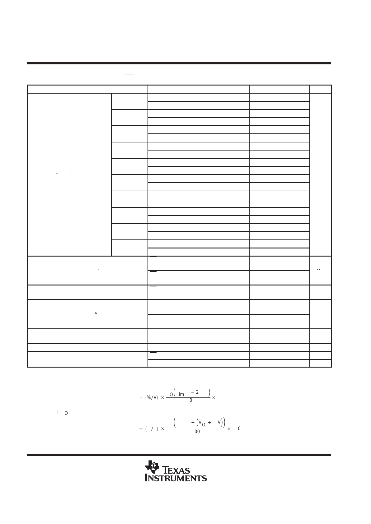
TYPICAL CHARACTERISTICS
Table of Graphs
FIGURE
p
vs Output current 1, 2, 3
VOOutput voltage
vs Free-air temperature 4, 5, 6
Ground current vs Free-air temperature 7
Output spectral noise density vs Frequency 8
Z
o
Output impedance vs Frequency 9
V
DO
Dropout voltage vs Free-air temperature 10
Ripple rejection vs Frequency 11
LDO startup time 12
Line transient response 13, 15
Load transient response 14, 16
vs Output current 17, 19
Equivalent series resistance (ESR)
vs Added ceramic capacitance 18, 20
TPS76901, TPS76912, TPS76915, TPS76918, TPS76925
TPS76927, TPS76928, TPS76930, TPS76933, TPS76950
ULTRALOW-POWER 100-mA LOW-DROPOUT LINEAR REGULATORS
SLVS203D – JUNE 1999 – REVISED APRIL 2000
6
POST OFFICE BOX 655303 • DALLAS, TEXAS 75265
TYPICAL CHARACTERISTICS
Figure 1
100
TPS76925
OUTPUT VOLTAGE
vs
OUTPUT CURRENT
2.496
2.488
2.482
20 60
2.494
2.490
2.486
40 80
2.498
0
– Output Voltage – V
V
O
2.492
2.484
VI = 3.5 V
CO = 4.7 µF
TA = 25° C
IO – Output Current – mA
Figure 2
IO – Output Current – mA
1.494
1.488
1.484
20 60
1.492
1.490
1.486
40 80
1.498
0 100
– Output Voltage – V
V
O
TPS76915
OUTPUT VOLTAGE
vs
OUTPUT CURRENT
1.496
VI = 2.7 V
CO = 4.7 µF
TA = 25° C
Figure 3
IO – Output Current – mA
TPS76933
OUTPUT VOLTAGE
vs
OUTPUT CURRENT
20 6040 800 100
– Output Voltage – V
V
O
3.280
3.274
3.270
3.278
3.276
3.272
3.284
3.282
VI = 4.3 V
CO = 4.7 µF
TA = 25° C
Figure 4
TA – Free-Air Temperature – °C
TPS76915
OUTPUT VOLTAGE
vs
FREE-AIR TEMPERATURE
1.486
1.480
–40 0
1.488
1.484
–20 20 140
1.496
–60
40 80
1.492
1.494
100 120
– Output Voltage – V
V
O
1.490
1.482
60
IO = 1 mA
VI = 2.7 V
CO = 4.7 µF
IO = 100 mA

TPS76901, TPS76912, TPS76915, TPS76918, TPS76925
TPS76927, TPS76928, TPS76930, TPS76933, TPS76950
ULTRALOW-POWER 100-mA LOW-DROPOUT LINEAR REGULATORS
SLVS203D – JUNE 1999 – REVISED APRIL 2000
7
POST OFFICE BOX 655303 • DALLAS, TEXAS 75265
TYPICAL CHARACTERISTICS
Figure 5
TA – Free-Air Temperature – °C
TPS76925
OUTPUT VOLTAGE
vs
FREE-AIR TEMPERATURE
2.476
2.492
2.486
2.496
– Output Voltage – V
V
O
2.478
2.490
2.480
2.494
2.482
–40 0–20 20 140–60 40 80 100 12060
IO = 1 mA
IO = 100 mA
VI = 3.5 V
CO = 4.7 µF
2.488
2.484
Figure 6
TA – Free-Air Temperature – °C
TPS76933
OUTPUT VOLTAGE
vs
FREE-AIR TEMPERATURE
3.265
3.260
3.255
3.270
3.285
3.275
3.280
– Output Voltage – V
V
O
–40 0–20 20 140–60 40 80 100 12060
IO = 100 mA
VI = 4.3 V
CO = 4.7 µF
IO = 1 mA
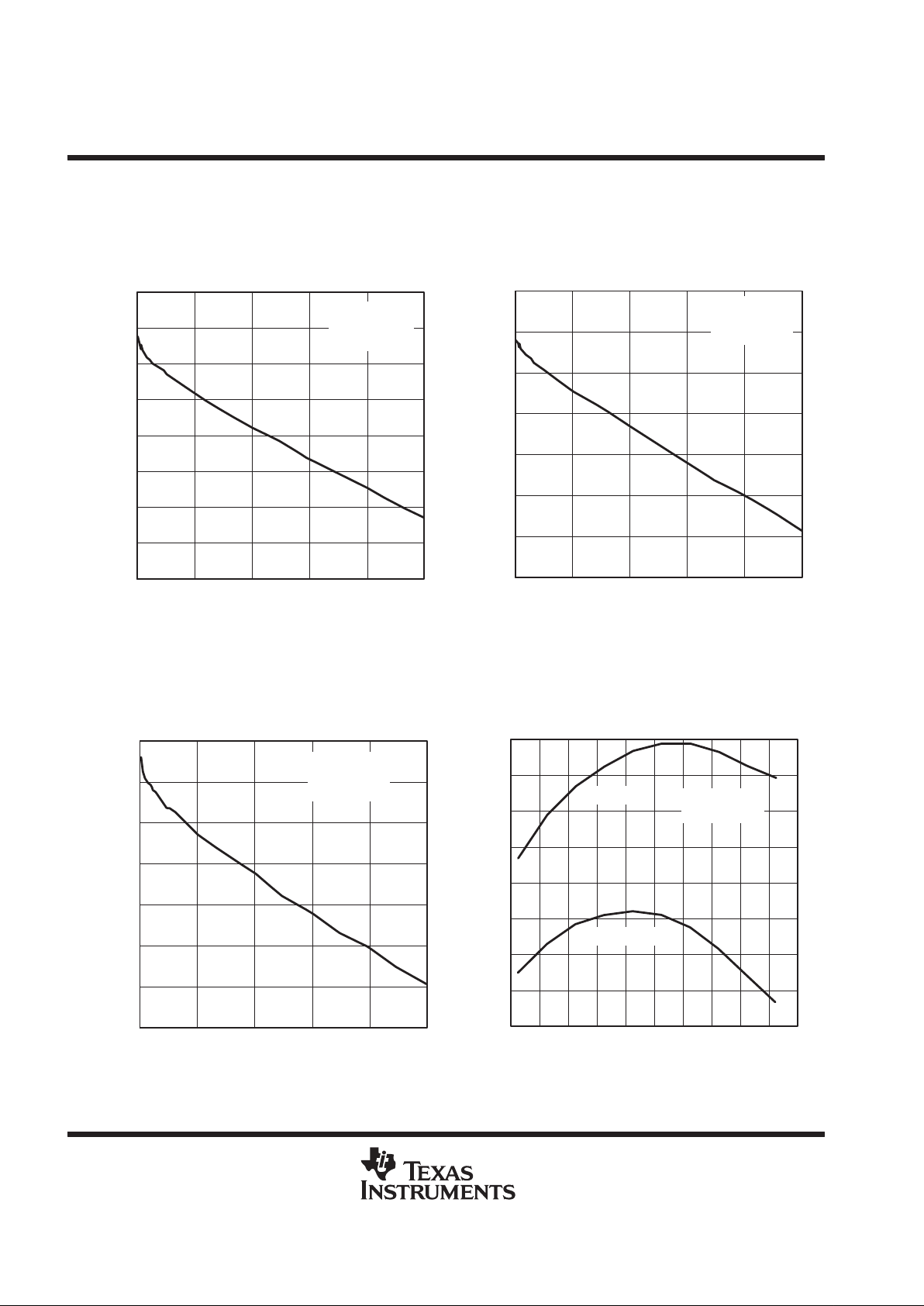
Figure 7
TA – Free-Air Temperature – °C
15
22
TPS76933
GROUND CURRENT
vs
FREE-AIR TEMPERATURE
Ground Current – Aµ
VI = 4.3 V
CO = 4.7 µF
–40 0–20 20 140–60 40 80 100 12060
21
20
19
18
17
16
IO = 0 mA
IO = 100 mA
Figure 8
f – Frequency – Hz
1k 10k 100k
CO = 10 µF
IO = 1 mA
VI = 4.3 V
0
1.6
1
2
0.2
1.4
0.4
1.8
0.6
1.2
0.8
100
CO = 4.7 µF
IO = 1 mA
CO = 4.7 µF
IO = 100 mA
CO = 10 µF
IO = 100 mA
V HzOutput Spectral Noise Density – µ
TPS76933
OUTPUT SPECTRAL NOISE DENSITY
vs
FREQUENCY

TPS76901, TPS76912, TPS76915, TPS76918, TPS76925
TPS76927, TPS76928, TPS76930, TPS76933, TPS76950
ULTRALOW-POWER 100-mA LOW-DROPOUT LINEAR REGULATORS
SLVS203D – JUNE 1999 – REVISED APRIL 2000
8
POST OFFICE BOX 655303 • DALLAS, TEXAS 75265
TYPICAL CHARACTERISTICS
Figure 9
100 1 M10 1 k
f – Frequency – Hz
10 k
– Output Impedance –Z
o
Ω
OUTPUT IMPEDANCE
vs
FREQUENCY
0
1.6
1
2
0.2
1.4
0.4
1.8
0.6
1.2
0.8
100 k
VI = 4.3 V
CO = 4.7 µF
ESR = 0.3 Ω
TA = 25° C
IO = 100 mA
IO = 1 mA
Figure 10
TA – Free-Air Temperature – °C
1
1000
10
100
VI = 3.2 V
CO = 4.7 µF
– Dropout Voltage – mV
V
DO
TPS76933
DROPOUT VOLTAGE
vs
FREE-AIR TEMPERATURE
–40 0–20 20 140–60 40 80 100 12060
IO = 10 mA
IO = 100 mA
Figure 11
10 M1 M100 k10 k1 k100
Ripple Rejection – dB
f – Frequency – Hz
RIPPLE REJECTION
vs
FREQUENCY
100
60
50
40
30
20
10
0
–10
10
TPS76933
VI = 4.3 V
CO = 4.7 µF
ESR = 0.3 Ω
70
80
90
IO = 100 mA
IO = 1 mA
Figure 12
LDO STARTUP TIME
t – Time – µs
0604020 80 100 140120 160 180 200
V
O
EN
TPS76901, TPS76912, TPS76915, TPS76918, TPS76925
TPS76927, TPS76928, TPS76930, TPS76933, TPS76950
ULTRALOW-POWER 100-mA LOW-DROPOUT LINEAR REGULATORS
SLVS203D – JUNE 1999 – REVISED APRIL 2000
9
POST OFFICE BOX 655303 • DALLAS, TEXAS 75265
TYPICAL CHARACTERISTICS
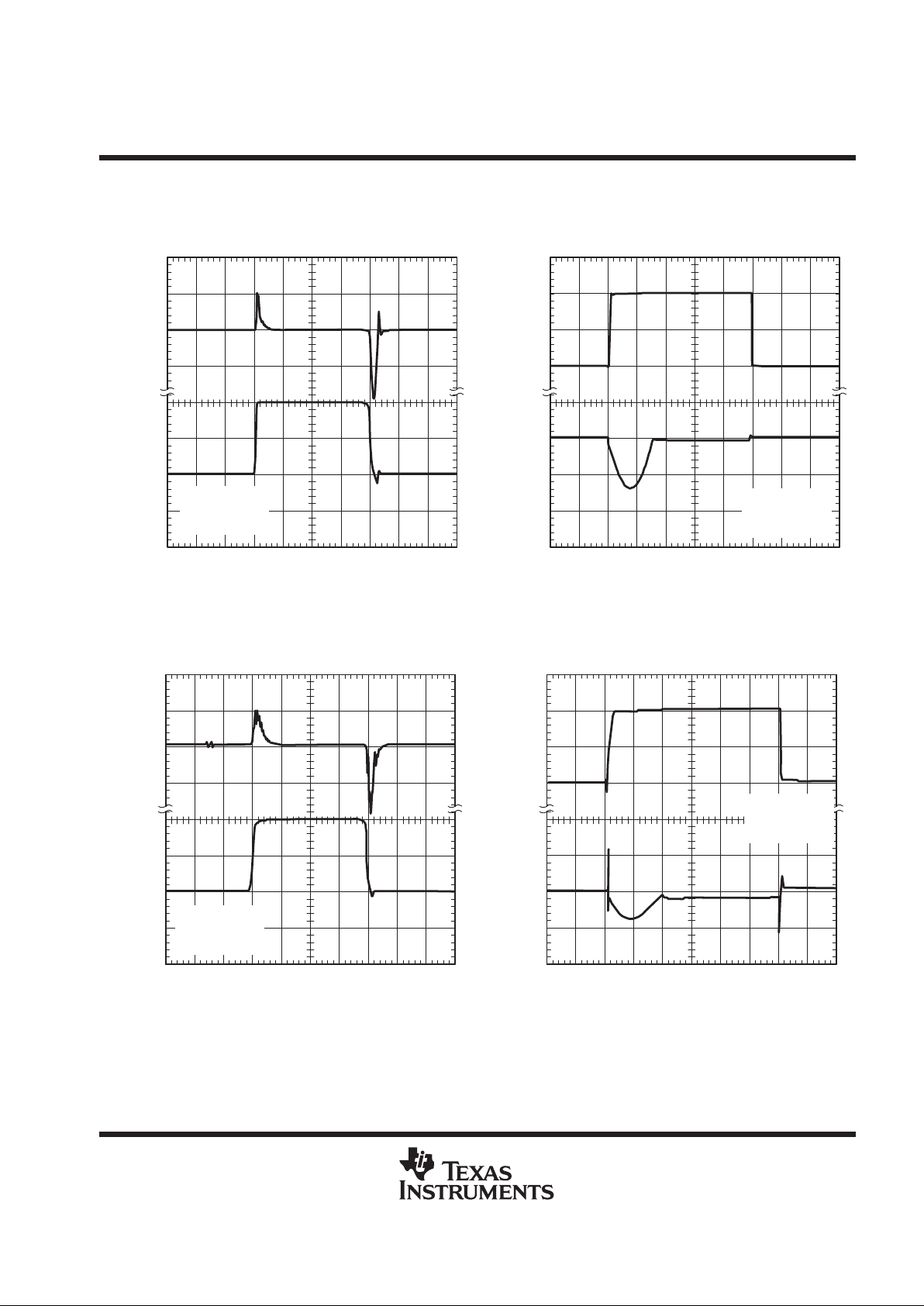
Figure 13
3.7
TPS76915
LINE TRANSIENT RESPONSE
V
O
t – Time – µs
0604020 80 100 140120 160 180 200
– Output Voltage – mV
IL = 10 mA
CO = 4.7 µF
ESR = 0.3 Ω
V
I
– Input Voltage – V
2.7
10
0
–10
Figure 14
t – Time – µs
TPS76915
LOAD TRANSIENT RESPONSE
0
0
0604020 80 100 140120 160 180 200
Current Load – mA
100
VI = 2.7 V
CO = 10 µF
ESR = 0.3 Ω
–200
–400
V
O
Output Voltage – mV
∆
– Change In
Figure 15
TPS76933
LINE TRANSIENT RESPONSE
t – Time – µs
5.3
V
O
0604020 80 100 140120 160 180
– Output Voltage – mVV
I
– Input Voltage – V
IL = 10 mA
CO = 4.7 µF
ESR = 0.3 Ω
4.3
10
0
–10
Figure 16
t – Time – µs
TPS76933
LOAD TRANSIENT RESPONSE
0
0604020 80 100 140120 160 180
Current Load – mA
100
VI = 4.3 V
CO = 4.7 µF
ESR = 0.3 Ω
100
0
–100
V
O
Output Voltage – mV
∆
– Change In

TPS76901, TPS76912, TPS76915, TPS76918, TPS76925
TPS76927, TPS76928, TPS76930, TPS76933, TPS76950
ULTRALOW-POWER 100-mA LOW-DROPOUT LINEAR REGULATORS
SLVS203D – JUNE 1999 – REVISED APRIL 2000
10
POST OFFICE BOX 655303 • DALLAS, TEXAS 75265
TYPICAL CHARACTERISTICS
Figure 17
1
0 25 50 75 100
100
IO – Output Current – mA
ESR – Equivalent Series Resistance – Ω
10
Region of Instability
VIN = 4.3 V
CO = 4.7 µF
3.3 V LDO
TPS76933
TYPICAL REGIONS OF STABILITY
EQUIVALENT SERIES RESISTANCE (ESR)
†
vs
OUTPUT CURRENT
0.1
Region of Stability
Figure 18
0 0.1 0.2 0.3 0.4 0.5
Added Ceramic Capacitance – µF
0.6 0.7 0.8 0.9 1
1
100
ESR – Equivalent Series Resistance – Ω
10
Region of Instability
Region of Stability
VIN = 4.3 V
CO = 4.7 µF
IL = 100 mA
TPS76933
TYPICAL REGIONS OF STABILITY
EQUIVALENT SERIES RESISTANCE (ESR)
vs
ADDED CERAMIC CAPACITANCE
Figure 19
IO – Output Current – mA
1
0 25 50 75 100
100
ESR – Equivalent Series Resistance – Ω
10
VIN = 4.3 V
CO = 10 µF
3.3 V LDO
TPS76933
TYPICAL REGIONS OF STABILITY
EQUIVALENT SERIES RESISTANCE (ESR)
†
vs
OUTPUT CURRENT
Region of Instability
Region of Stability
0.1
Figure 20
Added Ceramic Capacitance – µF
0 0.1 0.2 0.3 0.4 0.5 0.6 0.7 0.8 0.9 1
1
100
ESR – Equivalent Series Resistance – Ω
10
Region of Instability
Region of Stability
VIN = 4.3 V
CO = 10 µF
IL = 100 mA
TPS76933
TYPICAL REGIONS OF STABILITY
EQUIVALENT SERIES RESISTANCE (ESR)
vs
ADDED CERAMIC CAPACITANCE
TPS76901, TPS76912, TPS76915, TPS76918, TPS76925
TPS76927, TPS76928, TPS76930, TPS76933, TPS76950
ULTRALOW-POWER 100-mA LOW-DROPOUT LINEAR REGULATORS
SLVS203D – JUNE 1999 – REVISED APRIL 2000
11
POST OFFICE BOX 655303 • DALLAS, TEXAS 75265
APPLICATION INFORMATION
The TPS769xx family of low-dropout (LDO) regulators have been optimized for use in battery-operated
equipment. They feature extremely low dropout voltages, low quiescent current (17 µA nominally), and enable
inputs to reduce supply currents to 1 µA when the regulators are turned off.
device operation
The TPS769xx uses a PMOS pass element to dramatically reduce both dropout voltage and supply current over
more conventional PNP-pass-element LDO designs. The PMOS pass element is a voltage-controlled device
and, unlike a PNP transistor, it does not require increased drive current as output current increases. Supply
current in the TPS769xx is essentially constant from no load to maximum load.
Current limiting and thermal protection prevent damage by excessive output current and/or power dissipation.
The device switches into a constant-current mode at approximately 350 mA; further load reduces the output
voltage instead of increasing the output current. The thermal protection shuts the regulator off if the junction
temperature rises above approximately 165°C. Recovery is automatic when the junction temperature drops
approximately 25°C below the high temperature trip point. The PMOS pass element includes a back gate diode
that conducts reverse current when the input voltage level drops below the output voltage level.
A voltage of 1.7 V or greater on the EN
input will disable the TPS769xx internal circuitry, reducing the supply
current to 1µA. A voltage of less than 0.9 V on the EN input will enable the TPS769xx and will enable normal
operation to resume. The EN input does not include any deliberate hysteresis, and it exhibits an actual switching
threshold of approximately 1.5 V.
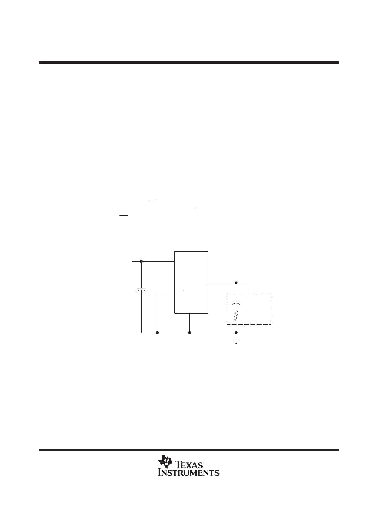
A typical application circuit is shown in Figure 21.
C1
1 µF
†
TPS76912, TPS76915, TPS76918, TPS76925, TPS76927, TPS76928,
TPS76930, TPS76933, TPS76950 (fixed-voltage options).
NC/FB
OUT
1
3
IN
EN
GND
2
4
5
V
I
ESR = 0.2 Ω
V
O
4.7 µF
+
TPS769xx
†
Figure 21. Typical Application Circuit
TPS76901, TPS76912, TPS76915, TPS76918, TPS76925
TPS76927, TPS76928, TPS76930, TPS76933, TPS76950
ULTRALOW-POWER 100-mA LOW-DROPOUT LINEAR REGULATORS
SLVS203D – JUNE 1999 – REVISED APRIL 2000
12
POST OFFICE BOX 655303 • DALLAS, TEXAS 75265
APPLICATION INFORMATION
external capacitor requirements
Although not required, a 0.047-µF or larger ceramic input bypass capacitor, connected between IN and GND
and located close to the TPS769xx, is recommended to improve transient response and noise rejection. A
higher-value electrolytic input capacitor may be necessary if large, fast-rise-time load transients are anticipated
and the device is located several inches from the power source.
Like all low dropout regulators, the TPS769xx requires an output capacitor connected between OUT and GND
to stabilize the internal control loop. The minimum recommended capacitance is 4.7 µF. The ESR (equivalent
series resistance) of the capacitor should be between 0.2 Ω and 10 Ω. to ensure stability . Capacitor values larger
than 4.7 µF are acceptable, and allow the use of smaller ESR values. Capacitances less than 4.7 µF are not
recommended because they require careful selection of ESR to ensure stability. Solid tantalum electrolytic,
aluminum electrolytic, and multilayer ceramic capacitors are all suitable, provided they meet the requirements
described above. Most of the commercially available 4.7 µF surface-mount solid tantalum capacitors, including
devices from Sprague, Kemet, and Nichico, meet the ESR requirements stated above. Multilayer ceramic
capacitors may have very small equivalent series resistances and may thus require the addition of a low value
series resistor to ensure stability.
CAP ACIT OR SELECTION
PART NO. MFR. VALUE MAX ESR
†
SIZE (H × L × W)
†
T494B475K016AS KEMET 4.7 µF 1.5 Ω 1.9 × 3.5 × 2.8
195D106x0016x2T SPRAGUE 10 µF 1.5 Ω 1.3 × 7.0 × 2.7
695D106x003562T SPRAGUE 10 µF 1.3 Ω 2.5 × 7.6 × 2.5
TPSC475K035R0600 AVX 4.7 µF 0.6 Ω 2.6 × 6.0 × 3.2
†
Size is in mm. ESR is maximum resistance in Ohms at 100 kHz and TA = 25°C. Contact manufacturer for minimum ESR values.
TPS76901, TPS76912, TPS76915, TPS76918, TPS76925
TPS76927, TPS76928, TPS76930, TPS76933, TPS76950
ULTRALOW-POWER 100-mA LOW-DROPOUT LINEAR REGULATORS
SLVS203D – JUNE 1999 – REVISED APRIL 2000
13
POST OFFICE BOX 655303 • DALLAS, TEXAS 75265
APPLICATION INFORMATION
output voltage programming
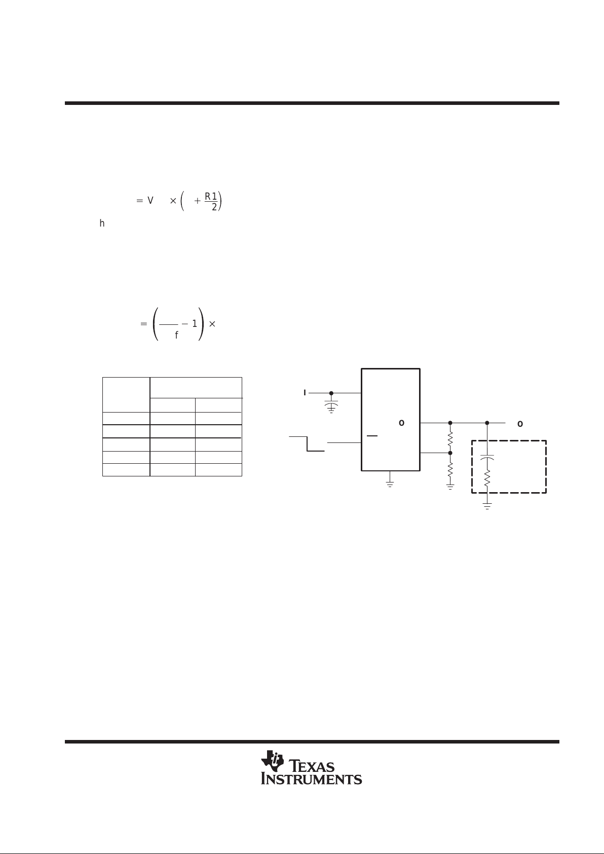
The output voltage of the TPS76901 adjustable regulator is programmed using an external resistor divider as
shown in Figure 22. The output voltage is calculated using:
VO+
V
ref
ǒ1
)
R1
R2
Ǔ
(1)
Where:
V
ref
= 1.224 V typ (the internal reference voltage)
Resistors R1 and R2 should be chosen for approximately 7-µA divider current. Lower value resistors can be
used but offer no inherent advantage and waste more power. Higher values should be avoided as leakage
currents at FB increase the output voltage error. The recommended design procedure is to choose
R2 = 169 kΩ to set the divider current at 7 µA and then calculate R1 using:
R1
+ ǒ
V
O
V
ref
*
1
Ǔ
R2
(2)
V
O
V
I
OUT
FB
R2
GND
EN
IN
≤0.9 V
≥1.7 V
TPS76901
1 µF
OUTPUT
VOLTAGE
(V)
R1 R2
2.5
3.3
3.6
4.0
5.0
174
287
324
383
523
169
169
169
169
169
OUTPUT VOLTAGE
PROGRAMMING GUIDE
DIVIDER RESISTANCE
(kΩ)
‡
‡
1% values shown.
3
1
4
2
R1
5
ESR = 0.2 Ω
4.7 µF
Figure 22. TPS76901 Adjustable LDO Regulator Programming

TPS76901, TPS76912, TPS76915, TPS76918, TPS76925
TPS76927, TPS76928, TPS76930, TPS76933, TPS76950
ULTRALOW-POWER 100-mA LOW-DROPOUT LINEAR REGULATORS
SLVS203D – JUNE 1999 – REVISED APRIL 2000
14
POST OFFICE BOX 655303 • DALLAS, TEXAS 75265
APPLICATION INFORMATION
power dissipation and junction temperature
Specified regulator operation is assured to a junction temperature of 125°C; the maximum junction temperature
should be restricted to 125°C under normal operating conditions. This restriction limits the power dissipation
the regulator can handle in any given application. T o ensure the junction temperature is within acceptable limits,
calculate the maximum allowable dissipation, P
D(max)
, and the actual dissipation, PD, which must be less than
or equal to P
D(max)
.
The maximum-power-dissipation limit is determined using the following equation:
P
D(max)
+
TJmax*T
A
R
q
JA
Where:
TJmax is the maximum allowable junction temperature
R
θJA
is the thermal resistance junction-to-ambient for the package, i.e., 285°C/W for the 5-terminal
SOT23.
T
A
is the ambient temperature.
The regulator dissipation is calculated using:
PD+ǒVI*
V
O
Ǔ
I
O
Power dissipation resulting from quiescent current is negligible. Excessive power dissipation will trigger the
thermal protection circuit.
regulator protection
The TPS769xx PMOS-pass transistor has a built-in back diode that conducts reverse current when the input
voltage drops below the output voltage (e.g., during power down). Current is conducted from the output to the
input and is not internally limited. If extended reverse voltage operation is anticipated, external limiting might
be appropriate.
The TPS769xx features internal current limiting and thermal protection. During normal operation, the TPS769xx
limits output current to approximately 350 mA. When current limiting engages, the output voltage scales back
linearly until the overcurrent condition ends. While current limiting is designed to prevent gross device failure,
care should be taken not to exceed the power dissipation ratings of the package. If the temperature of the device
exceeds approximately 165°C, thermal-protection circuitry shuts it down. Once the device has cooled down to
below approximately 140°C, regulator operation resumes.

TPS76901, TPS76912, TPS76915, TPS76918, TPS76925
TPS76927, TPS76928, TPS76930, TPS76933, TPS76950
ULTRALOW-POWER 100-mA LOW-DROPOUT LINEAR REGULATORS
SLVS203D – JUNE 1999 – REVISED APRIL 2000
15
POST OFFICE BOX 655303 • DALLAS, TEXAS 75265
MECHANICAL DATA
DBV (R-PDSO-G5) PLASTIC SMALL-OUTLINE PACKAGE
0,25
0,35
0,55
Gage Plane
0,15 NOM
4073253-4/B 10/97
2,50
3,00
0,40
0,20
1,50
1,80
45
3
3,10
1
2,70
1,00
1,30
0,05 MIN
Seating Plane
0,10
0,95
M
0,25
0°–8°
NOTES: A. All linear dimensions are in millimeters.
B. This drawing is subject to change without notice.
C. Body dimensions include mold flash or protrusion.

IMPORTANT NOTICE
T exas Instruments and its subsidiaries (TI) reserve the right to make changes to their products or to discontinue
any product or service without notice, and advise customers to obtain the latest version of relevant information
to verify, before placing orders, that information being relied on is current and complete. All products are sold
subject to the terms and conditions of sale supplied at the time of order acknowledgment, including those
pertaining to warranty, patent infringement, and limitation of liability.
TI warrants performance of its semiconductor products to the specifications applicable at the time of sale in
accordance with TI’s standard warranty. Testing and other quality control techniques are utilized to the extent
TI deems necessary to support this warranty. Specific testing of all parameters of each device is not necessarily
performed, except those mandated by government requirements.
Customers are responsible for their applications using TI components.
In order to minimize risks associated with the customer’s applications, adequate design and operating
safeguards must be provided by the customer to minimize inherent or procedural hazards.
TI assumes no liability for applications assistance or customer product design. TI does not warrant or represent
that any license, either express or implied, is granted under any patent right, copyright, mask work right, or other
intellectual property right of TI covering or relating to any combination, machine, or process in which such
semiconductor products or services might be or are used. TI’s publication of information regarding any third
party’s products or services does not constitute TI’s approval, warranty or endorsement thereof.
Copyright 2000, Texas Instruments Incorporated
 Loading...