

Texas Instruments TPS70758PWPR, TPS70758PWP, TPS70751PWPR, TPS70751PWP, TPS70748PWPR Datasheet
...
TPS70745, TPS70748, TPS70751, TPS70758, TPS70702
DUAL-OUTPUT LOW-DROPOUT VOLTAGE REGULATORS
WITH POWER UP SEQUENCING FOR SPLIT VOLTAGE DSP SYSTEMS
SLVS291 – MAY 2000
1
POST OFFICE BOX 655303 • DALLAS, TEXAS 75265
D
Dual Output Voltages for Split-Supply
Applications
D
Selectable Power Up Sequencing for DSP
Applications
D
Output Current Range of 250 mA on
Regulator 1 and 125 mA on Regulator 2
D
Fast Transient Response
D
Voltage Options are 3.3-V/2.5-V, 3.3-V/1.8-V,
3.3-V/1.5-V, 3.3-V/1.2-V, and Dual Adjustable
Outputs
D
Open Drain Power-On Reset With 120-ms
Delay
D
Open Drain Power Good for Regulator 1
D
Ultra Low 190 µA (typ) Quiescent Current
D
1 µA Input Current During Standby
D
Low Noise: 65 µV
RMS
Without Bypass
Capacitor
D
Quick Output Capacitor Discharge Feature
D
Two Manual Reset Inputs
D
2% Accuracy Over Load and Temperature
D
Undervoltage Lockout (UVLO) Feature
D
20-Pin PowerP AD TSSOP Package
D
Thermal Shutdown Protection
description
TPS707xx family devices are designed to provide
a complete power management solution for DSP,
processor power, ASIC, FPGA, and digital
applications where dual output voltage regulators
are required. Easy programmability of the
sequencing function makes this family ideal for
any DSP applications with power sequencing
requirement. Differentiated features, such as
accuracy, fast transient response, SVS supervisory circuit (power on reset), manual reset inputs,
and enable function, provide a complete system
solution.
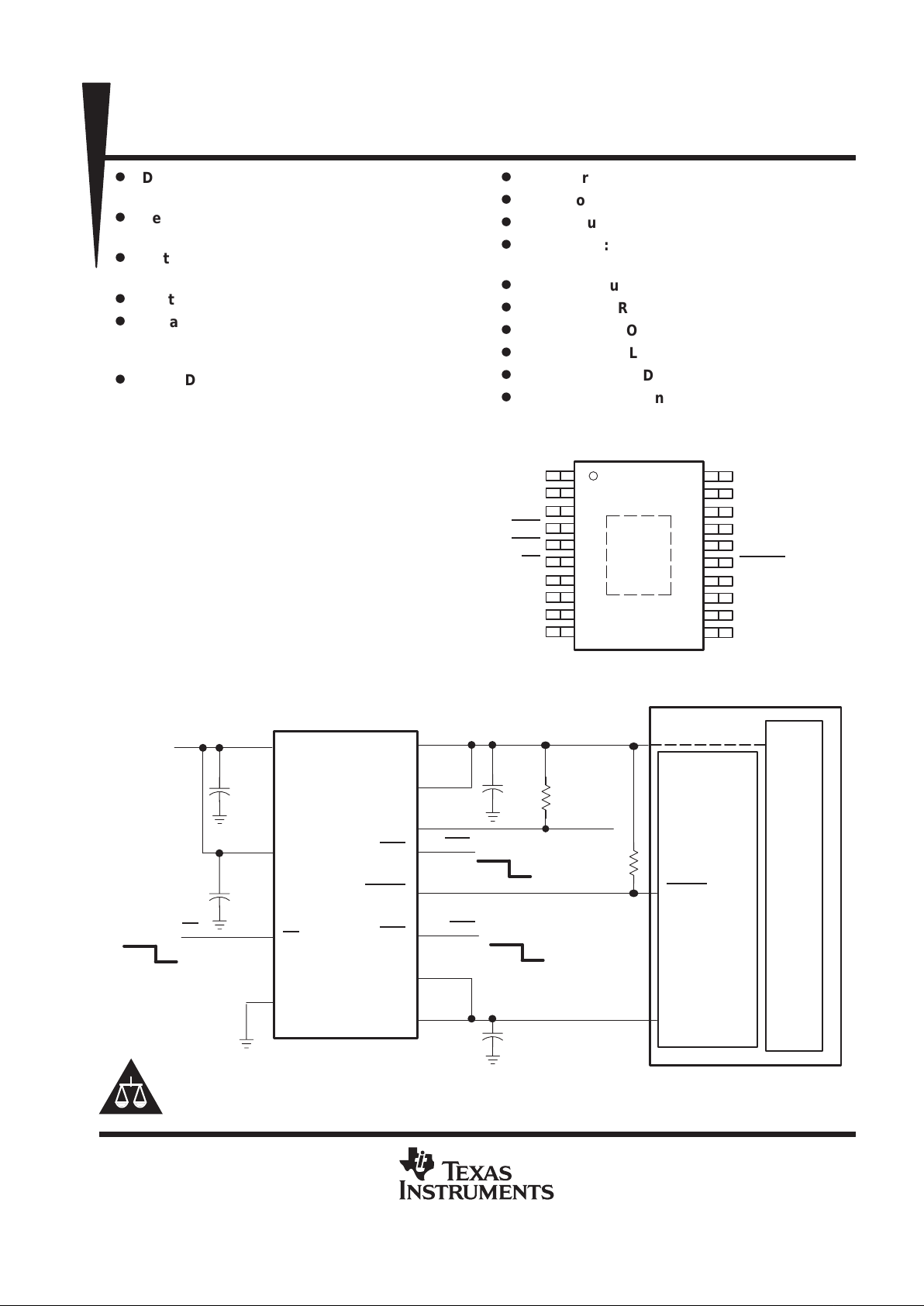
1.8 V
V
IN1
V
IN2
EN
SEQ
V
OUT1
V
SENSE1
PG1
MR2
RESET
MR1
V
SENSE2
V
OUT2
TPS70751 PWP
5 V
3.3 V
I/O
MR1
Core
0.1 µF
RESET
10 µF
10 µF
0.1 µF
DSP
MR2
PG1
EN
250 kΩ
>2 V
<0.7 V
250 kΩ
>2 V
<0.7 V
>2 V
<0.7 V
PRODUCTION DATA information is current as of publication date.
Products conform to specifications per the terms of Texas Instruments
standard warranty. Production processing does not necessarily include
testing of all parameters.
Please be aware that an important notice concerning availability, standard warranty, and use in critical applications of
Texas Instruments semiconductor products and disclaimers thereto appears at the end of this data sheet.
PowerPAD is a trademark of Texas Instruments Incorporated.
1
2
3
4
5
6
7
8
9
10
20
19
18
17
16
15
14
13
12
11
PWP PACKAGE
(TOP VIEW)
NC
V
IN1
V
IN1
MR1
MR2
EN
SEQ
GND
V
IN2
V
IN2
NC
V
OUT1
V
OUT1
V
SENSE1
/FB1
PG1
RESET
V
SENSE2
/FB2
V
OUT2
V
OUT2
NC
Copyright 2000, Texas Instruments Incorporated
TPS70745, TPS70748, TPS70751, TPS70758, TPS70702
DUAL-OUTPUT LOW-DROPOUT VOLTAGE REGULATORS
WITH POWER UP SEQUENCING FOR SPLIT VOLTAGE DSP SYSTEMS
SLVS291 – MAY 2000
2
POST OFFICE BOX 655303 • DALLAS, TEXAS 75265
description (continued)
The TPS707xx family of voltage regulators offers very low dropout voltage and dual outputs with power up
sequence control, which is designed primarily for DSP applications. These devices have extremely low noise
output performance without using any added filter bypass capacitors and are designed to have a fast transient
response and be stable with 10 uF low ESR capacitors.
These devices have fixed 3.3-V/2.5-V , 3.3-V/1.8-V , 3.3-V/1.5-V , 3.3-V/1.2-V, and adjustable/adjustable voltage
options. Regulator 1 can support up to 250 mA and regulator 2 can support up to 125 mA. Separate voltage
inputs allow the designer to configure the source power.
Because the PMOS device behaves as a low-value resistor, the dropout voltage is very low (typically 83 mV
on regulator 1) and is directly proportional to the output current. Additionally , since the PMOS pass element is
a voltage-driven device, the quiescent current is very low and independent of output loading (maximum of
230 µA over the full range of output current). This LDO family also features a sleep mode; applying a high signal
to EN
(enable) shuts down both regulators, reducing the input current to 1 µA at TJ = 25°C.
The device is enabled when the EN pin is connected to a low-level input voltage. The output voltages of the two
regulators are sensed at the V
SENSE1
and V
SENSE2
pins respectively.
The input signal at the SEQ pin controls the power-up sequence of the two regulators. When the device is
enabled and the SEQ terminal is pulled high or left open, V
OUT2
will turn on first and V
OUT1
will remain off until
V
OUT2
reaches approximately 83% of its regulated output voltage. At that time V
OUT1
will be turned on. If V
OUT2
is pulled below 83% (i.e. over load condition) V
OUT1
will be turned off. Pulling the SEQ terminal low , reverses
the power-up order and V
OUT1
will be turned on first. The SEQ pin is connected to an internal pullup current
source.
For each regulator, there is an internal discharge transistor to discharge the output capacitor when the regulator
is turned off(disabled).
The PG1 pin reports the voltage conditions at VOUT1. Power good can be used to implement a SVS for the
circuitry supplied by regulator 1.
The TPS707xx features a RESET
(SVS, POR, or Power On Reset). RESET output initiates a reset in DSP
systems and related digital applications in the event of an undervoltage condition. RESET
indicates the status
of V
OUT2
and both manual reset pins (MR1 and MR2). When V
OUT2
reaches 95% of its regulated voltage and
MR1 and MR2 are in the logic high state, RESET will go to a high impedance state after 120 ms delay . RESET
will go to logic low state when V
OUT2
regulated output voltage is pulled below 95% (i.e. over load condition) of
its regulated voltage. To monitor V
OUT1
, the PG1 output pin can be connected to MR1 or MR2.
The device has an undervoltage lockout UVLO circuit which prevents the internal regulators from turning on until
VIN1 reaches 2.5V.
AVAILABLE OPTIONS
T
J
REGULATOR 1
VO (V)
REGULATOR 2
VO (V)
TSSOP
(PWP)
3.3 V 1.2 V TPS70745PWP
3.3 V 1.5 V TPS70748PWP
°
°
3.3 V 1.8 V TPS70751PWP
–
40°C to 125°C
3.3 V 2.5 V TPS70758PWP
Adjustable
(1.22 V to 5.5 V)
Adjustable
(1.22 V to 5.5 V)
TPS70702PWP
NOTE: The TPS70702 is programmable using external resistor dividers (see
application information) The PWP package is available taped and reeled. Add
an R suffix to the device type (e.g., TPS70702PWPR).
TPS70745, TPS70748, TPS70751, TPS70758, TPS70702
DUAL-OUTPUT LOW-DROPOUT VOLTAGE REGULATORS
WITH POWER UP SEQUENCING FOR SPLIT VOLTAGE DSP SYSTEMS
SLVS291 – MAY 2000
3
POST OFFICE BOX 655303 • DALLAS, TEXAS 75265
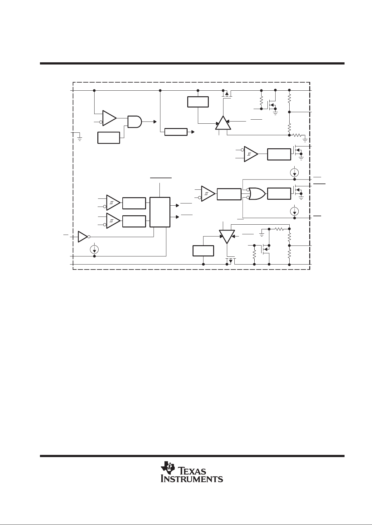
detailed block diagram – fixed voltage version
UVLO
Thermal
Shutdown
Shutdown
2.5 V
+–
Current
Sense
Reference
VREF
VREF
ENA_1
10 kΩ
Rising Edge
Deglitch
0.95 × VREF
FB2
Falling Edge
Delay
V
IN1
0.95 × VREF
FB1
Rising Edge
Deglitch
Falling Edge
Deglitch
0.83 × VREF
FB2
UV Comp
Falling Edge
Deglitch
0.83 × VREF
FB1
UV Comp
Power
Sequence
Logic
SHUTDOWN
ENA_1
ENA_2
V
IN1
Current
Sense
+–
10 kΩ
ENA_2
ENA_2
FB2
VREF
VIN1 (2 Pins)
GND
EN
SEQ
(see Note B)
VIN2 (2 Pins)
VOUT1 (2 Pins)
VSENSE1
(see Note A)
PG1
MR2
RESET
MR1
VSENSE2
(see Note A)
VOUT2(2 Pins)
FB1
V
IN1
ENA_1
NOTES: A. For most applications, V
SENSE1
and V
SENSE2
should be externally connected to V
OUT
as close as possible to the device.
For other implementations, refer to SENSE terminal connection discussion in the application information section.
B. If the SEQ terminal is floating at the input, V
OUT2
will power up first.
TPS70745, TPS70748, TPS70751, TPS70758, TPS70702
DUAL-OUTPUT LOW-DROPOUT VOLTAGE REGULATORS
WITH POWER UP SEQUENCING FOR SPLIT VOLTAGE DSP SYSTEMS
SLVS291 – MAY 2000
4
POST OFFICE BOX 655303 • DALLAS, TEXAS 75265
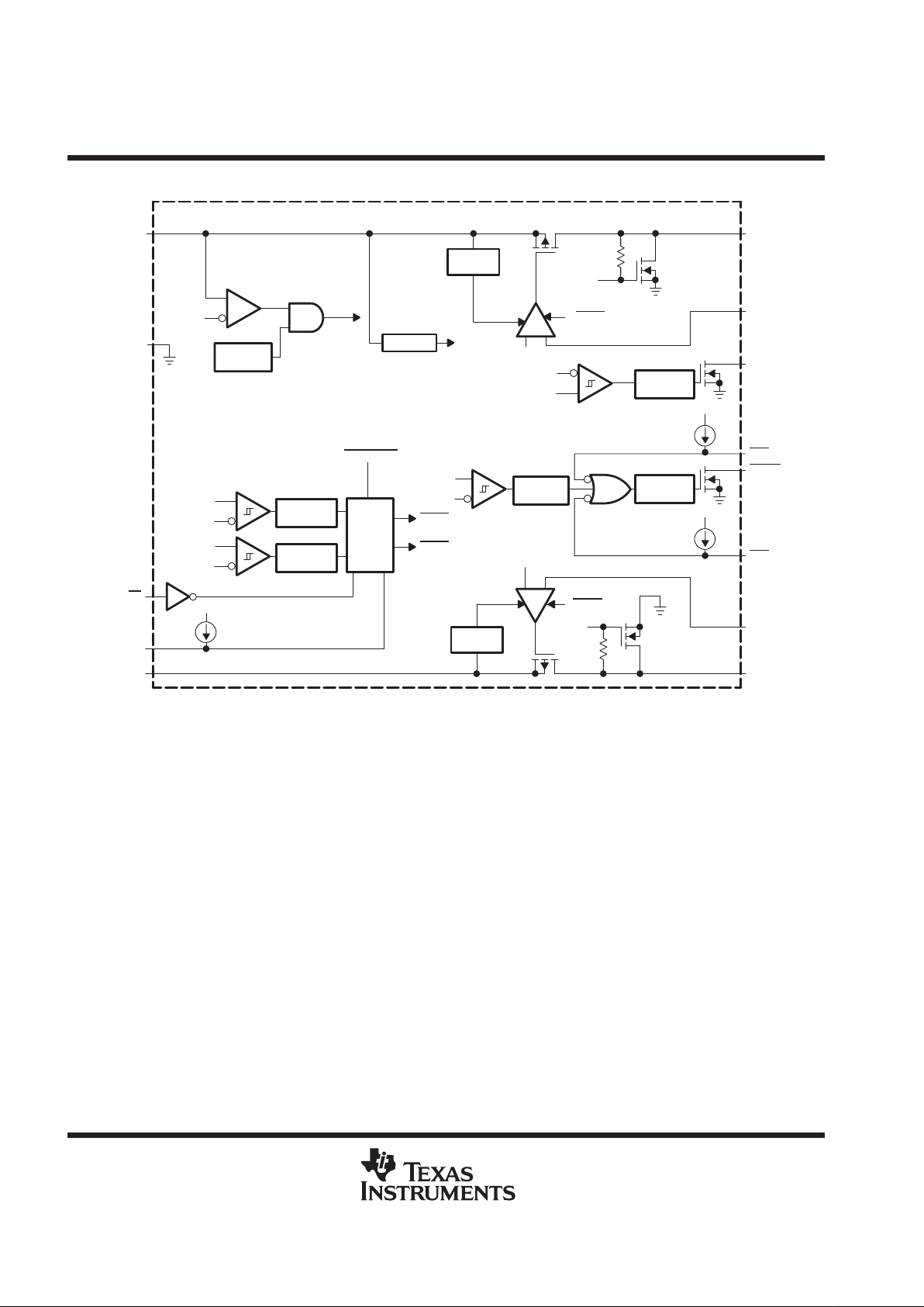
detailed block diagram – adjustable voltage version
UVLO
Thermal
Shutdown
Shutdown
2.5 V
+–
Current
Sense
Reference
VREF
VREF
ENA_1
ENA_1
Rising Edge
Deglitch
0.95 × VREF
FB2
Falling Edge
Delay
V
IN1
0.95 × VREF
FB1
Rising Edge
Deglitch
Falling Edge
Deglitch
0.83 × VREF
FB2
UV Comp
Falling Edge
Deglitch
0.83 × VREF
FB1
UV Comp
Power
Sequence
Logic
SHUTDOWN
ENA_1
ENA_2
V
IN1
Current
Sense
+–
ENA_2
ENA_2
VREF
VIN1 (2 Pins)
GND
EN
SEQ
(see Note B)
VIN2 (2 Pins)
VOUT1 (2 Pins)
FB1
(see Note A)
PG1
MR2
RESET
MR1
FB2
(see Note A)
VOUT2 (2 Pins)
V
IN1
NOTES: A. For most applications, FB1 and FB2 should be externally connected to resistor dividers as close as possible to the device.
For other implementations, refer to FB terminals connection discussion in the application information section.
B. If the SEQ terminal is floating at the input, V
OUT2
will power up first.
TPS70745, TPS70748, TPS70751, TPS70758, TPS70702
DUAL-OUTPUT LOW-DROPOUT VOLTAGE REGULATORS
WITH POWER UP SEQUENCING FOR SPLIT VOLTAGE DSP SYSTEMS
SLVS291 – MAY 2000
5
POST OFFICE BOX 655303 • DALLAS, TEXAS 75265
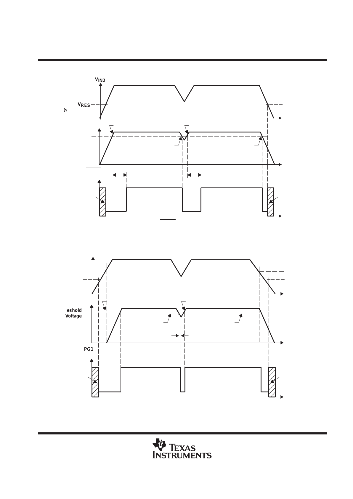
RESET timing diagram (with V
IN1
powered up and MR1 AND MR2 at logic high)
NOTES: A. V
RES
is the minimum input voltage for a valid RESET . The symbol V
res
is not currently listed within EIA or JEDEC standards
for semiconductor symbology.
V
IN2
V
RES
(see Note A)
V
RES
t
t
t
V
OUT2
Threshold
Voltage
RESET
Output
120 ms
Delay
120 ms
Delay
Output
Undefined
Output
Undefined
V
IT+
(see Note B)
V
IT–
(see Note B)
V
IT+
(see Note B)
B. VIT –Trip voltage is typically 5% lower than the output voltage (95%VO) V
IT–
to V
IT+
is the hysteresis voltage.
V
IT–
(see Note B)
PG1 timing diagram
NOTES: A. V
PG1
is the minimum input voltage for a valid PG1. The symbol V
PG1
is not currently listed within EIA or JEDEC
standards for semiconductor symbology.
V
PG1
t
t
t
Threshold
Voltage
PG1
Output
Output
Undefined
Output
Undefined
V
IT+
(see Note B)V
IT+
(see Note B)
B. VIT –Trip voltage is typically 5% lower than the output voltage (95%VO) V
IT–
to V
IT+
is the hysteresis voltage.
V
IN1
V
OUT2
V
PG1
(see Note A)
V
IT–
(see Note B)
V
IT–
(see Note B)
V
UVLO
V
UVLO
30 µs
TPS70745, TPS70748, TPS70751, TPS70758, TPS70702
DUAL-OUTPUT LOW-DROPOUT VOLTAGE REGULATORS
WITH POWER UP SEQUENCING FOR SPLIT VOLTAGE DSP SYSTEMS
SLVS291 – MAY 2000
6
POST OFFICE BOX 655303 • DALLAS, TEXAS 75265
Terminal Functions
TERMINAL
NAME
NO.
I/O
DESCRIPTION
EN 6 I Active low enable
GND 8 Ground
MR1 4 I Manual reset input 1, active low, pulled up internally
MR2 5 I Manual reset input 2, active low, pulled up internally
NC 1, 11, 20 No connection
PG1 16 O Open drain output, low when V
OUT1
voltage is less than 95% of the nominal regulated voltage
RESET 15 O Open drain output, SVS (power on reset) signal, active low
SEQ 7 I Power up sequence control: SEQ=High, V
OUT2
powers up first; SEQ=Low, V
OUT1
powers up first, SEQ
terminal pulled up internally .
V
IN1
2, 3 I Input voltage of regulator 1
V
IN2
9, 10 I Input voltage of regulator 2
V
OUT1
18, 19 O Output voltage of regulator 1
V
OUT2
12, 13 O Output voltage of regulator 2
V
SENSE2
/FB2 14 I Regulator 2 output voltage sense/ regulator 2 feedback for adjustable
V
SENSE1
/FB1 17 I Regulator 1 output voltage sense/ regulator 1 feedback for adjustable
absolute maximum ratings over operating junction temperature (unless otherwise noted)
†
Input voltage range‡:V
IN1
–0.3 V to 7 V. . . . . . . . . . . . . . . . . . . . . . . . . . . . . . . . . . . . . . . . . . . . . . . . . . . . . . . . . .
V
IN2
–0.3 V to 7 V. . . . . . . . . . . . . . . . . . . . . . . . . . . . . . . . . . . . . . . . . . . . . . . . . . . . . . . . . .
Voltage range at EN –0.3 V to 7 V. . . . . . . . . . . . . . . . . . . . . . . . . . . . . . . . . . . . . . . . . . . . . . . . . . . . . . . . . . . . . . . .
Output voltage range (V
OUT1
, V
SENSE1
) 5.5 V. . . . . . . . . . . . . . . . . . . . . . . . . . . . . . . . . . . . . . . . . . . . . . . . . . . .
Output voltage range (V
OUT2
, V
SENSE2
) 5.5 V. . . . . . . . . . . . . . . . . . . . . . . . . . . . . . . . . . . . . . . . . . . . . . . . . . . .
Maximum RESET, PG1 voltage 7 V. . . . . . . . . . . . . . . . . . . . . . . . . . . . . . . . . . . . . . . . . . . . . . . . . . . . . . . . . . . . . . .
Maximum MR1, MR2, and SEQ voltage V
IN1
. . . . . . . . . . . . . . . . . . . . . . . . . . . . . . . . . . . . . . . . . . . . . . . . . . . . . . .
Peak output current Internally limited. . . . . . . . . . . . . . . . . . . . . . . . . . . . . . . . . . . . . . . . . . . . . . . . . . . . . . . . . . . . . .
Continuous total power dissipation See Dissipation Rating Tables. . . . . . . . . . . . . . . . . . . . . . . . . . . . . . . . . . . .
Operating virtual junction temperature range, T
J
–40°C to 125°C. . . . . . . . . . . . . . . . . . . . . . . . . . . . . . . . . . . . .
Storage temperature range, T
stg
–65°C to 150°C. . . . . . . . . . . . . . . . . . . . . . . . . . . . . . . . . . . . . . . . . . . . . . . . . . .
ESD rating, HBM 2 kV. . . . . . . . . . . . . . . . . . . . . . . . . . . . . . . . . . . . . . . . . . . . . . . . . . . . . . . . . . . . . . . . . . . . . . . . . .
†
Stresses beyond those listed under “absolute maximum ratings” may cause permanent damage to the device. These are stress ratings only, and
functional operation of the device at these or any other conditions beyond those indicated under “recommended operating conditions” is not
implied. Exposure to absolute-maximum-rated conditions for extended periods may affect device reliability.
‡
All voltages are tied to network ground.
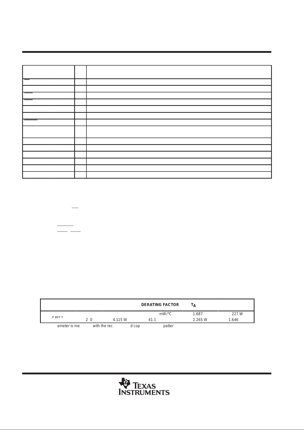
DISSIPATION RATING TABLE
PACKAGE
AIR FLOW
(CFM)
TA ≤ 25°C
ÁÁÁÁ
Á
DERATING FACTOR TA = 70°C TA = 85°C
0
3.067 W
30.67 mW/°C
1.687 W
1.227 W
PWP
§
250 4.115 W
41.15 mW/°C 2.265 W 1.646 W
§
This parameter is measured with the recommended copper heat sink pattern on a 4-layer PCB, 1 oz. copper on 4-in × 4-in
ground layer. For more information, refer to TI technical brief SLMA002.
TPS70745, TPS70748, TPS70751, TPS70758, TPS70702
DUAL-OUTPUT LOW-DROPOUT VOLTAGE REGULATORS
WITH POWER UP SEQUENCING FOR SPLIT VOLTAGE DSP SYSTEMS
SLVS291 – MAY 2000
7
POST OFFICE BOX 655303 • DALLAS, TEXAS 75265
recommended operating conditions
MIN MAX UNIT
Input voltage, V
I
†
2.7 6 V
Output current, IO (regulator 1) 0 250 mA
Output current, IO (regulator 2) 0 125 mA
Output voltage range (for adjustable option) 1.22 5.5 V
Operating virtual junction temperature, T
J
–40 125 °C
†
To calculate the minimum input voltage for maximum output current, use the following equation: V
I(min)
= V
O(max)
+ V
DO(max load)
.
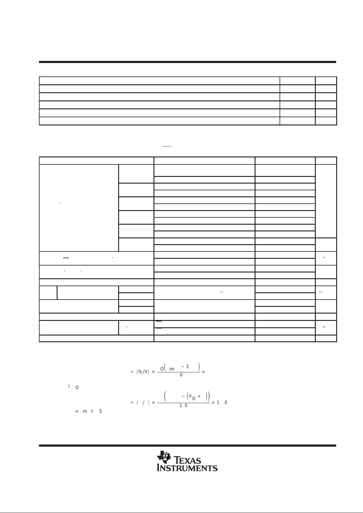
electrical characteristics over recommended operating junction temperature (TJ = –40°C to 125°C)
V
IN1
or V
IN2
= V
O(nom)
+ 1 V, I
O
= 1 mA, EN = 0, CO = 33 µF(unless otherwise noted)
PARAMETER TEST CONDITIONS MIN TYP MAX UNIT
Reference
2.7 V < VI < 6 V, FB connected to V
O
TJ = 25°C
1.22
voltage
2.7 V < VI < 6 V, FB connected to V
O
1.196 1.244
p
2.7 V < VI < 6 V, TJ = 25°C 1.2
1.2 V Output
2.7 V < VI < 6 V 1.176 1.224
p
2.7 V < VI < 6 V, TJ = 25°C 1.5
V
V
Output voltage
1.5 V Output
2.7 V < VI < 6 V 1.47 1.53
O
(see Notes 1 and 3)
p
2.8 V < VI < 6 V, TJ = 25°C 1.8
1.8 V Output
2.8 V < VI < 6 V 1.764 1.836
p
3.5 V < VI < 6 V, TJ = 25°C 2.5
2.5 V Output
3.5 V < VI < 6 V 2.45 2.55
p
4.3 V < VI < 6 V, TJ = 25°C 3.3
3.3 V Output
4.3 V < VI < 6 V 3.234 3.366
V
Quiescent current (GND current) for regulator 1 and
See Note 3, TJ = 25°C 190
()g
regulator 2, EN = 0 V, (see Note 1)
See Note 3 230
µA
Output voltage line regulation (∆V/V) for
VO + 1 V < VI ≤ 6 V, TJ = 25°C, See Note 1 0.01%
gg(
OO
)
regulator 1 and regulator 2 (see Note 2)
VO + 1 V < VI ≤ 6 V, See Note 1 0.1%
V
Load regulation for V
OUT1
and V
OUT2
TJ = 25°C, See Note 3 1 mV
p
Regulator 1
°
65
VnOutput noise voltage
Regulator 2
BW
=
300 Hz to 50 kHz
,
C
O
=
33 µF
,
T
J
=
25°C
65
µVrms
p
Regulator 1
1.6 1.9
Output current limit
Regulator 2
V
O
=
0 V
0.750 1
A
Thermal shutdown junction temperature 150 °C
Regulator 1 and
EN = VI,T
J
= 25°C 2
I
I(standby)
Standby current
g
Regulator 2
EN = V
I
6
µA
PSRR Power supply ripple rejection f = 1 kHz, CO = 33 µF, TJ = 25°C, See Note 1 60 dB
NOTES: 1. Minimum input operating voltage is 2.7 V or V
O(typ)
+ 1 V, whichever is greater . Maximum input voltage = 6 V , minimum output current
1 mA.
2. If VO < 1.8 V then V
imax
= 6 V, V
Imin
= 2.7 V:
Line Regulation (mV)
+ǒ%ńVǓ
V
O
ǒ
V
imax
*
2.7 V
Ǔ
100
1000
If VO > 2.5 V then V
imax
= 6 V, V
Imin
= Vo + 1 V :
Line Regulation (mV)
+ǒ%ńVǓ
V
O
ǒ
V
imax
*ǒVO)
1
Ǔ
Ǔ
100
1000
3. IO = 1 mA to 250 mA for Regulator 1 and 1 mA to 125 mA for Regulator 2.
TPS70745, TPS70748, TPS70751, TPS70758, TPS70702
DUAL-OUTPUT LOW-DROPOUT VOLTAGE REGULATORS
WITH POWER UP SEQUENCING FOR SPLIT VOLTAGE DSP SYSTEMS
SLVS291 – MAY 2000
8
POST OFFICE BOX 655303 • DALLAS, TEXAS 75265
electrical characteristics over recommended operating junction temperature (TJ = –40°C to 125°C)
V
IN1
or V
IN2
= V
O(nom)
+ 1 V, IO = 1 mA, EN = 0, CO = 33 µF(unless otherwise noted) (continued)
PARAMETER TEST CONDITIONS MIN TYP MAX UNIT
Minimum input voltage for valid RESET I
(RESET)
= 300 µA, V
(RESET)
≤ 0.8 V 1.0 1.3 V
Trip threshold voltage VO decreasing 92% 95% 98% V
O
Hysteresis voltage Measured at V
O
0.5% V
O
RESET
t
(RESET)
RESET pulse duration 80 120 160 ms
t
r(RESET)
Rising edge deglitch 30 µs
Output low voltage VI = 3.5 V, I
(RESET)
= 1 mA 0.15 0.4 V
Leakage current V
(RESET)
= 6 V 1 µA
Minimum input voltage for valid PG1 I
O(PG1)
= 300 µA, V
(PG1
) ≤ 0.8 V 1.0 1.3 V
Trip threshold voltage VO decreasing 92% 95% 98% V
O
Hysteresis voltage Measured at V
O
0.5% V
O
PG1
t
f(PG1)
Falling edge deglitch 30 µs
Output low voltage VI = 2.7 V, I
(PG1)
= 1 mA 0.15 0.4 V
Leakage current V
(PG1)
= 6 V 1 µA
High level EN input voltage 2 V
EN
Low level EN input voltage 0.7 V
Input current (EN) –1 1 µA
High level SEQ input voltage 2 V
SEQ
Low level SEQ input voltage 0.7 V
SEQ pull up current source 6 µA
High level input voltage 2 V
MR1 / MR2
Low level input voltage 0.7 V
Pull up current source 6 µA
V
OUT2
UV comparator – positive-going input
threshold voltage of V
OUT1
UV comparator
80% VO83% VO86% V
O
V
V
OUT2
UV comparator – hysteresis 0.5% V
O
mV
V
OUT2
V
OUT2
UV comparator – falling edge deglitch V
SENSE_2
decreasing below threshold 140 µs
Peak output current 2 ms pulse width 375 mA
Discharge transistor current V
OUT2
= 1.5 V 7.5 mA
V
OUT1
UV comparator – positive-going input
threshold voltage of V
OUT1
UV comparator
80% VO83% VO86% V
O
V
V
OUT1
UV comparator – hysteresis 0.5% V
O
mV
V
OUT1
UV comparator – falling edge deglitch V
SENSE_1
decreasing below threshold 140 µs
V
OUT1
Dropout voltage (see Note 4)
IO = 250 mA, V
IN1
= 3.2 V,
TJ = 25°C
83
m
V
g( )
IO = 250 mA, V
IN1
= 3.2 V 140
Peak output current 2 ms pulse width 750 mA
Discharge transistor current V
OUT1
= 1.5 V 7.5 mA
VOUT1 UVLO UVLO threshold 2.4 2.65 V
FB Input current – TPS70702 FB = 1.8 V 1 µA
NOTE 4: Input voltage(V
IN1
or V
IN2
) = VO(Typ) – 100 mV . For the 1.5 V , 1.8 V and 2.5 V regulators, the dropout voltage is limited by input voltage
range. The 3.3 V regulator input voltage is to 3.2 V to perform this test.
TPS70745, TPS70748, TPS70751, TPS70758, TPS70702
DUAL-OUTPUT LOW-DROPOUT VOLTAGE REGULATORS
WITH POWER UP SEQUENCING FOR SPLIT VOLTAGE DSP SYSTEMS
SLVS291 – MAY 2000
9
POST OFFICE BOX 655303 • DALLAS, TEXAS 75265
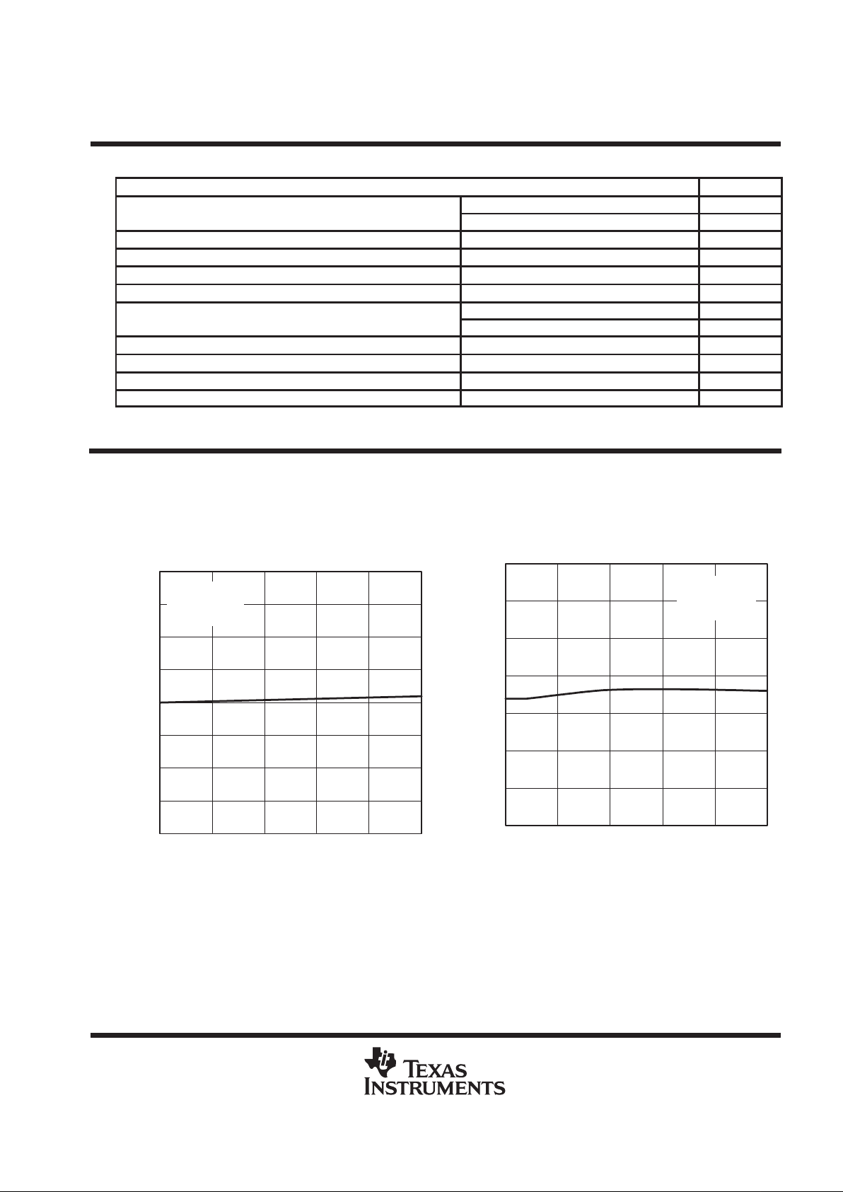
Table of Graphs
FIGURE
p
vs Output current 1 – 3
VOOutput voltage
vs Junction temperature 4 – 7
Ground current vs Junction temperature 8
PSRR Power supply rejection ratio vs Frequency 9 – 12
Output spectral noise density vs Frequency 13 – 16
Z
o
Output impedance vs Frequency 17 – 20
p
vs Junction temperature 21, 22
Dropout voltage
vs Input voltage 23, 24
Load transient response 25, 26
Line transient response 27, 28
Output voltage vs Time (start-up) 29, 30
Stability Equivalent series resistance (ESR) vs Output current 32 – 35
TYPICAL CHARACTERISTICS
Figure 1
IO – Output Current – A
3.299
3.298
3.296
3.295
0 0.05 0.1 0.15
– Output Voltage – V
3.301
3.302
TPS70751
OUTPUT VOLTAGE
vs
OUTPUT CURRENT
3.303
0.2 0.25
3.3
3.297
V
O
V
IN1
= 4.3 V
TJ = 25°C
V
OUT1
Figure 2
1.799
1.797
1.796
1.795
0 0.025 0.05 0.075
1.800
1.801
1.802
0.1 0.12
5
1.798
IO – Output Current – A
– Output Voltage – V
TPS70751
OUTPUT VOLTAGE
vs
OUTPUT CURRENT
V
O
V
IN2
= 2.8V
TJ = 25°C
V
OUT2
TPS70745, TPS70748, TPS70751, TPS70758, TPS70702
DUAL-OUTPUT LOW-DROPOUT VOLTAGE REGULATORS
WITH POWER UP SEQUENCING FOR SPLIT VOLTAGE DSP SYSTEMS
SLVS291 – MAY 2000
10
POST OFFICE BOX 655303 • DALLAS, TEXAS 75265
TYPICAL CHARACTERISTICS
1.198
1.197
1.196
1.195
0 0.025 0.05 0.075
1.199
1.200
1.201
0.1 0.125
IO – Output Current – A
– Output Voltage – V
TPS70745
OUTPUT VOLTAGE
vs
OUTPUT CURRENT
V
O
V
IN2
= 2.7 V
TJ = 25°C
V
OUT2
Figure 3
Figure 4
TJ – Junction Temperature – °C
3.23
3.25
3.27
3.29
3.31
3.33
3.35
TPS70751
OUTPUT VOLTAGE
vs
JUNCTION TEMPERATURE
– Output Voltage – VV
O
–40 –25 –10 5 20 35 50 65 80 95 110 125
V
IN1
= 4.3 V
IO = 1 mA
V
OUT1
Figure 5
TJ – Junction Temperature – °C
3.23
3.25
3.27
3.29
3.31
3.33
3.35
TPS70751
OUTPUT VOLTAGE
vs
JUNCTION TEMPERATURE
– Output Voltage – VV
O
–40 –25 –10 5 20 35 50 65 80 95 110 125
V
IN1
= 4.3 V
IO = 250 mA
V
OUT1
TPS70745, TPS70748, TPS70751, TPS70758, TPS70702
DUAL-OUTPUT LOW-DROPOUT VOLTAGE REGULATORS
WITH POWER UP SEQUENCING FOR SPLIT VOLTAGE DSP SYSTEMS
SLVS291 – MAY 2000
11
POST OFFICE BOX 655303 • DALLAS, TEXAS 75265
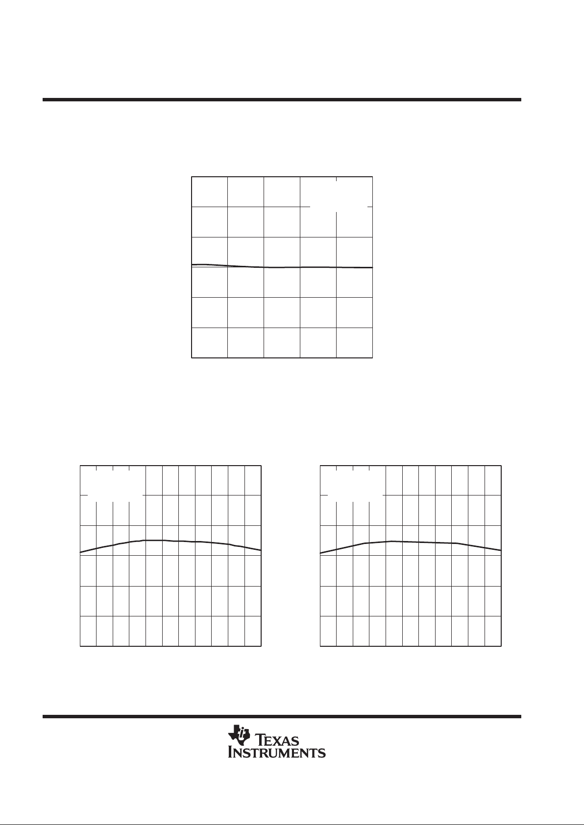
TYPICAL CHARACTERISTICS
Figure 6
1.786
1.788
1.790
1.792
1.794
1.796
1.798
1.800
TJ – Junction Temperature – °C
TPS70751
OUTPUT VOLTAGE
vs
JUNCTION TEMPERATURE
– Output Voltage – VV
O
–40 –25 –10 5 20 35 50 65 80 95 110 125
V
IN2
= 2.8 V
IO = 1 mA
V
OUT2
Figure 7
1.790
1.791
1.792
1.793
1.794
1.795
1.796
1.797
1.798
1.799
TJ – Junction Temperature – °C
TPS70751
OUTPUT VOLTAGE
vs
JUNCTION TEMPERATURE
– Output Voltage – VV
O
–40 –25 –10 5 20 35 50 65 80 95 110 125
V
IN2
= 2.8 V
IO = 125 mA
V
OUT2
150
160
170
180
–40 –25 –10 5 20 35 50 65 80
TJ – Junction Temperature – °C
95 110 125
190
200
210
GROUND CURRENT
vs
JUNCTION TEMPERATURE
I
OUT1
= 1 mA
I
OUT2
= 1 mA
Ground Current – Aµ
Regulator 1 and Regulator 2
I
OUT1
= 250 mA
I
OUT2
= 125 mA
Figure 8
TPS70745, TPS70748, TPS70751, TPS70758, TPS70702
DUAL-OUTPUT LOW-DROPOUT VOLTAGE REGULATORS
WITH POWER UP SEQUENCING FOR SPLIT VOLTAGE DSP SYSTEMS
SLVS291 – MAY 2000
12
POST OFFICE BOX 655303 • DALLAS, TEXAS 75265
TYPICAL CHARACTERISTICS
Figure 9
IO = 10 mA
CO = 22 µF
V
OUT1
–60
–80
–90
10 100 1 k 10 k
–40
–20
–10
100 k 1 M
–30
–50
–70
PSRR – Power Supply Rejection Ratio – dB
f – Frequency – Hz
TPS70751
POWER SUPPLY REJECTION RATIO
vs
FREQUENCY
Figure 10
–40
–60
–70
–90
10 100 1 k 10 k
–20
0
10
100 k 1 M
–10
–30
–50
–80
IO = 250 mA
CO = 22 µF
V
OUT1
PSRR – Power Supply Rejection Ratio – dB
f – Frequency – Hz
TPS70751
POWER SUPPLY REJECTION RATIO
vs
FREQUENCY
Figure 11
–60
–80
–90
10 100 1 k 10 k
–40
–20
–10
100 k 1 M
–30
–50
–70
PSRR – Power Supply Rejection Ratio – dB
f – Frequency – Hz
TPS70751
POWER SUPPLY REJECTION RATIO
vs
FREQUENCY
IO = 10 mA
CO = 22 µF
V
OUT2
Figure 12
–40
–60
–70
–90
10 100 1 k 10 k
–20
0
10
100 k 1 M
–10
–30
–50
–80
IO = 150 mA
CO = 22 µF
V
OUT2
PSRR – Power Supply Rejection Ratio – dB
f – Frequency – Hz
TPS70751
POWER SUPPLY REJECTION RATIO
vs
FREQUENCY

TPS70745, TPS70748, TPS70751, TPS70758, TPS70702
DUAL-OUTPUT LOW-DROPOUT VOLTAGE REGULATORS
WITH POWER UP SEQUENCING FOR SPLIT VOLTAGE DSP SYSTEMS
SLVS291 – MAY 2000
13
POST OFFICE BOX 655303 • DALLAS, TEXAS 75265
TYPICAL CHARACTERISTICS
Figure 13
0.01
0.1
1
10
100 1 k 10 k 100 k
f – Frequency – Hz
OUTPUT SPECTRAL NOISE DENSITY
vs
FREQUENCY
V
IN1
= 4.3 V
V
OUT1
= 3.3 V
IO = 10 mA
V HzOutput Spectral Noise Density – µ
Figure 14
0.01
0.1
1
10
100 1 k 10 k 100 k
f – Frequency – Hz
OUTPUT SPECTRAL NOISE DENSITY
vs
FREQUENCY
V
IN1
= 4.3 V
V
OUT1
= 3.3 V
IO = 250 mA
V HzOutput Spectral Noise Density – µ
Figure 15
0.01
0.1
1
10
100 1 k 10 k 100 k
f – Frequency – Hz
OUTPUT SPECTRAL NOISE DENSITY
vs
FREQUENCY
V
IN2
= 2.8 V
V
OUT2
= 1.8 V
IO = 10 mA
V HzOutput Spectral Noise Density – µ
Figure 16
0.01
0.1
1
10
100 1 k 10 k 100 k
f – Frequency – Hz
OUTPUT SPECTRAL NOISE DENSITY
vs
FREQUENCY
V
IN2
= 2.8 V
V
OUT2
= 1.8 V
IO = 125 mA
V HzOutput Spectral Noise Density – µ

TPS70745, TPS70748, TPS70751, TPS70758, TPS70702
DUAL-OUTPUT LOW-DROPOUT VOLTAGE REGULATORS
WITH POWER UP SEQUENCING FOR SPLIT VOLTAGE DSP SYSTEMS
SLVS291 – MAY 2000
14
POST OFFICE BOX 655303 • DALLAS, TEXAS 75265
TYPICAL CHARACTERISTICS
Figure 17
10 100 1 k 10 k
– Output Impedance –
f – Frequency – Hz
OUTPUT IMPEDANCE
vs
FREQUENCY
100 k 1 M 10 M
Z
O
Ω
10
1
0.1
0.01
CO = 33 µF
IO = 250 mA
V
OUT1
= 3.3 V
TJ = 25°C
Figure 18
CO = 33 µF
IO = 10 mA
V
OUT1
= 3.3 V
TJ = 25°C
10 100 1 k 10 k
– Output Impedance –
10
f – Frequency – Hz
OUTPUT IMPEDANCE
vs
FREQUENCY
100
100 k 1 M 10 M
1
0.1
0.01
Z
O
Ω
Figure 19
10
1
0.1
10 100 1 k 10 k
– Output Impedance –
f – Frequency – Hz
OUTPUT IMPEDANCE
vs
FREQUENCY
100 k 1 M 10 M
Z
O
Ω
CO = 33 µF
IO = 125 mA
V
OUT2
= 1.8 V
TJ = 25°C
Figure 20
CO = 33 µF
IO = 10 mA
V
OUT2
= 1.8 V
TJ = 25°C
10 100 1 k 10 k
– Output Impedance –
10
f – Frequency – Hz
OUTPUT IMPEDANCE
vs
FREQUENCY
100
100 k 1 M 10 M
1
0.1
0.01
Z
O
Ω

TPS70745, TPS70748, TPS70751, TPS70758, TPS70702
DUAL-OUTPUT LOW-DROPOUT VOLTAGE REGULATORS
WITH POWER UP SEQUENCING FOR SPLIT VOLTAGE DSP SYSTEMS
SLVS291 – MAY 2000
15
POST OFFICE BOX 655303 • DALLAS, TEXAS 75265
TYPICAL CHARACTERISTICS
Figure 21
TJ – Junction Temperature – °C
Dropout Voltage – mV
DROPOUT VOLTAGE
vs
JUNCTION TEMPERATURE
–40 –25 –10 5 20 35 50 65 80 95 110 125
CO = 33 µF
V
IN1
= 3.2 V
0
40
60
80
100
120
20
IO = 250 mA
Figure 22
0
1
2
3
4
5
6
TJ – Junction Temperature – °C
Dropout Voltage – mV
DROPOUT VOLTAGE
vs
JUNCTION TEMPERATURE
–40 –25 –10 5 20 35 50 65 80 95 110 125
IO = 10 mA
IO = 0 mA
CO = 33 µF
V
IN1
= 3.2 V
Figure 23
0
20
40
80
100
120
2.5 3 3.5 4 4.5 5
VI – Input Voltage – V
Dropout Voltage – mV
IO = 250 mA
V
OUT1
140
TJ = 125°C
TJ = 25°C
TJ= –40°C
TPS70702
DROPOUT VOLTAGE
vs
INPUT VOLTAGE
60
Figure 24
0
50
100
150
200
250
2.5 3 3.5 4 4.5 5
VI – Input Voltage – V
Dropout Voltage – mV
IO = 125 mA
V
OUT2
TJ = 125°C
TJ = 25°C
TJ = –40°C
TPS70702
DROPOUT VOLTAGE
vs
INPUT VOLTAGE

TPS70745, TPS70748, TPS70751, TPS70758, TPS70702
DUAL-OUTPUT LOW-DROPOUT VOLTAGE REGULATORS
WITH POWER UP SEQUENCING FOR SPLIT VOLTAGE DSP SYSTEMS
SLVS291 – MAY 2000
16
POST OFFICE BOX 655303 • DALLAS, TEXAS 75265
TYPICAL CHARACTERISTICS
Figure 25
0 0.2 0.4 0.6 0.8 1 1.2 1.4 1.6 1.8 2
20
LOAD TRANSIENT RESPONSE
250
– Output Current – mA
V
O
– Change in∆
Output Voltage – mV I
O
t – Time – ms
CO = 33 µF
TJ = 25°C
V
OUT1
= 3.3 V
0
0
–20
–40
Figure 26
0 0.2 0.4 0.6 0.8 1 1.2 1.4 1.6 1.8 2
20
LOAD TRANSIENT RESPONSE
0
– Output Current – mA
V
O
– Change in∆
Output Voltage – mV I
O
t – Time – ms
125
0
–20
CO = 33 µF
TJ = 25°C
V
OUT2
= 1.8 V
–40
–60
–80
Figure 27
0 20 40 60 80 100 120
5.3
LINE TRANSIENT RESPONSE
4.3
140 160 180 200
– Input Voltage – V
V
I
t – Time – µs
IO = 250 mA
CO = 33 µF
V
OUT1
0
50
–50
V
O
– Change in∆
Output Voltage – mV
Figure 28
0 20 40 60 80 100 120
LINE TRANSIENT RESPONSE
2.8
140 160 180 200
– Input Voltage – V
V
I
t – Time – µs
IO = 125 mA
CO = 33 µF
V
OUT2
V
O
– Change in∆
Output Voltage – mV
0
10
–10
3.8

TPS70745, TPS70748, TPS70751, TPS70758, TPS70702
DUAL-OUTPUT LOW-DROPOUT VOLTAGE REGULATORS
WITH POWER UP SEQUENCING FOR SPLIT VOLTAGE DSP SYSTEMS
SLVS291 – MAY 2000
17
POST OFFICE BOX 655303 • DALLAS, TEXAS 75265
TYPICAL CHARACTERISTICS
Figure 29
t – Time – ms
OUTPUT VOLTAGE
vs
TIME (START-UP)
VO = 3.3 V
CO = 33 µF
IO = 250 mA
V
OUT1
SEQ = Low
02
–5
2
3
1
0
0
5
0.2 1.81.61.41.210.4 0.6 0.8
– Output Voltage
V
O
OUT1
(V ) – V
Enable Voltage – V
Figure 30
VO = 1.8 V
CO = 33 µF
IO = 125 mA
V
OUT2
SEQ = High
t – Time – ms
OUTPUT VOLTAGE
vs
TIME (START-UP)
02
–5
1
2
0
–1
0
5
0.2 1.81.61.41.210.4 0.6 0.8
Enable Voltage – V
– Output Voltage
V
O
OUT2
(V ) – V
IN
EN
OUT
+
GND
C
O
ESR
R
L
V
I
To Load
R
Figure 31. Test Circuit for Typical Regions of Stability
†
Equivalent series resistance (ESR) refers to the total series resistance, including the ESR of the capacitor, any series resistance added
externally, and PWB trace resistance to CO.

TPS70745, TPS70748, TPS70751, TPS70758, TPS70702
DUAL-OUTPUT LOW-DROPOUT VOLTAGE REGULATORS
WITH POWER UP SEQUENCING FOR SPLIT VOLTAGE DSP SYSTEMS
SLVS291 – MAY 2000
18
POST OFFICE BOX 655303 • DALLAS, TEXAS 75265
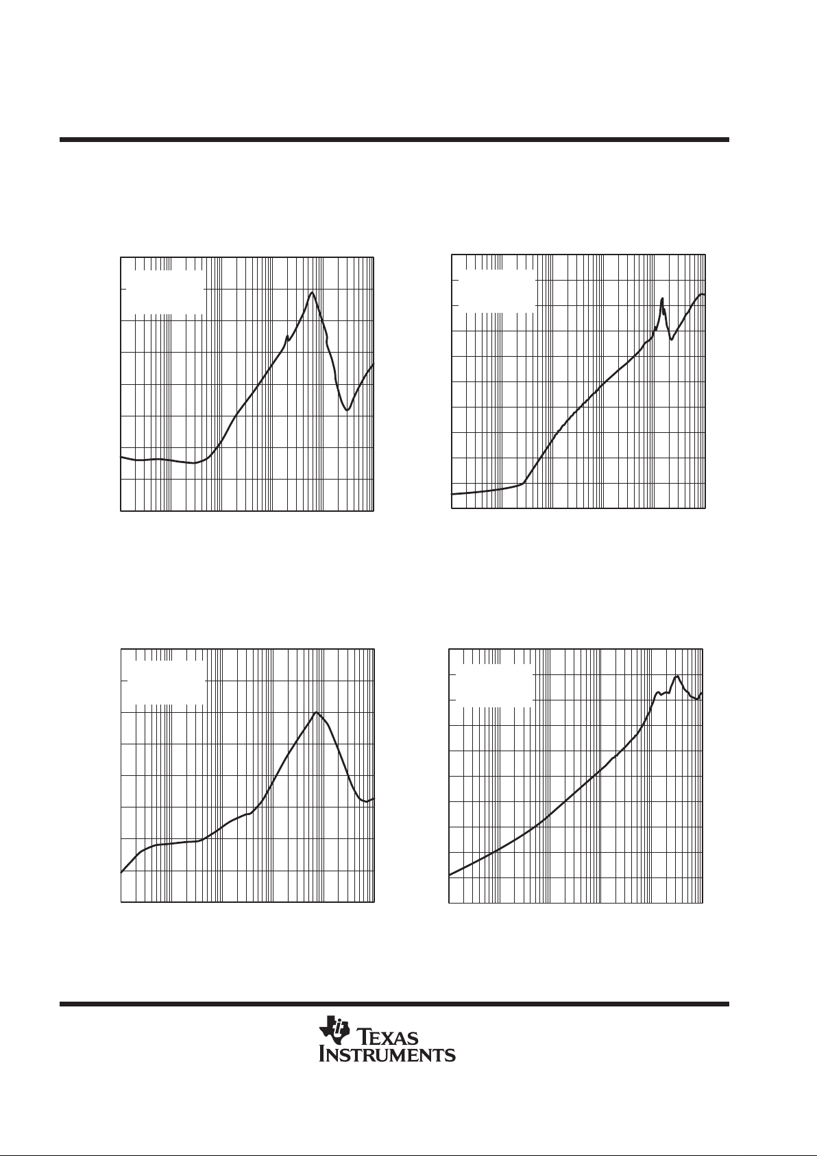
TYPICAL CHARACTERISTICS
Figure 32
IO – Output Current – mA
TYPICAL REGION OF STABILITY
EQUIVALENT SERIES RESISTANCE
†
vs
OUTPUT CURRENT
ESR – Equivalent Series Resistance – Ω
0.1
0.01
0 50 100 150 200 250
10
1
VO = 3.3 V
CO = 10 µF
TJ = 25°C
REGION OF INSTABILITY
REGION OF INSTABILITY
50 mΩ
Figure 33
IO – Output Current – mA
TYPICAL REGION OF STABILITY
EQUIVALENT SERIES RESISTANCE
†
vs
OUTPUT CURRENT
ESR – Equivalent Series Resistance – Ω
0 50 100 150 200 250
REGION OF INSTABILITY
0.1
10
1
250 mΩ
VO = 3.3 V
CO = 6.8 µF
TJ = 25°C
REGION OF INSTABILITY
Figure 34
IO – Output Current – mA
TYPICAL REGION OF STABILITY
EQUIVALENT SERIES RESISTANCE
†
vs
OUTPUT CURRENT
ESR – Equivalent Series Resistance – Ω
0.1
0.01
0 25 50 75 100 125
10
1
REGION OF INSTABILITY
50 mΩ
REGION OF INSTABILITY
VO = 1.8 V
CO = 10 µF
TJ = 25°C
Figure 35
IO – Output Current – mA
TYPICAL REGION OF STABILITY
EQUIVALENT SERIES RESISTANCE
†
vs
OUTPUT CURRENT
ESR – Equivalent Series Resistance – Ω
0 25 50 75 100 125
REGION OF INSTABILITY
0.1
1
VO = 1.8 V
CO = 6.8 µF
TJ = 25°C
10
REGION OF INSTABILITY
250 mΩ
†
Equivalent series resistance (ESR) refers to the total series resistance, including the ESR of the capacitor, any series resistance added
externally, and PWB trace resistance to CO.

TPS70745, TPS70748, TPS70751, TPS70758, TPS70702
DUAL-OUTPUT LOW-DROPOUT VOLTAGE REGULATORS
WITH POWER UP SEQUENCING FOR SPLIT VOLTAGE DSP SYSTEMS
SLVS291 – MAY 2000
19
POST OFFICE BOX 655303 • DALLAS, TEXAS 75265
detailed description
The TPS707xx low dropout regulator family provides dual regulated output voltages for DSP applications that
require a high-performance power management solution. These devices provide fast transient response and
high accuracy with small output capacitors, while drawing low quiescent current. Programmable sequencing
provides a power solution for DSPs without any external component requirements. This reduces the component
cost and board space while increasing total system reliability . TPS707xx family has an enable feature which puts
the device in sleep mode reducing the input currents to less than 3 µA. Other features are integrated SVS (power
on reset, RESET
) and power good (PG1) that monitor output voltages and provide logic output to the system.
These differentiated features provide a complete DSP power solution.
The TPS707xx, unlike many other LDOs, feature very low quiescent current which remains virtually constant
even with varying loads. Conventional LDO regulators use a pnp pass element, the base current of which is
directly proportional to the load current through the regulator (I
B
= IC/β). The TPS707xx uses a PMOS transistor
to pass current; because the gate of the PMOS is voltage driven, operating current is low and stable over the
full load range.
pin functions
enable
The EN terminal is an input which enables or shuts down the device. If EN is at a voltage high signal the device
will be in shutdown mode. When the EN goes to voltage low, then the device will be enabled.
sequence
The SEQ terminal is an input that programs which output voltage (V
OUT1
or V
OUT2
) will be turned on first. When
the device is enabled and the SEQ terminal is pulled high or left open, V
OUT2
will turn on first and V
OUT1
will
remain off until V
OUT2
reaches approximately 83% of its regulated output voltage. At that time the V
OUT1
will
be turned on. If V
OUT2
is pulled below 83% (i.e., over load condition) V
OUT1
will be turned off. This terminal has
a 6-µA pullup current to V
IN1
.
Pulling the SEQ terminal low reverses the power-up order and V
OUT1
will be turned on first. For detail timing
diagrams refer to Figures 36 and 42.
power–good
The PG1 terminal is an open drain, active high output terminal which indicates the status of the V
OUT1
regulator.
When the V
OUT1
reaches 95% of its regulated voltage, PG1 goes into a high impedance state. PG1 goes into
a low impedance state when V
OUT1
is pulled below 95% (i.e. over-load condition) of its regulated voltage. The
open drain output of the PG1 terminal requires a pullup resistor
.
manual reset pins (MR1 and MR2)
MR1 and MR2 are active low input terminals used to trigger a reset condition. When either MR1 or MR2 is pulled
to logic low, a POR (RESET) will occur. These terminals have a 6-µA pullup current to V
IN1
.
sense (V
SENSE1
, V
SENSE2
)
The sense terminals of fixed-output options must be connected to the regulator output, and the connection
should be as short as possible. Internally, sense connects to high-impedance wide-bandwidth amplifiers
through a resistor-divider network and noise pickup feeds through to the regulator output. It is essential to route
the sense connection in such a way to minimize/avoid noise pickup. Adding RC networks between the V
SENSE
terminals and V
OUT
terminals to filter noise is not recommended because it can cause the regulators to oscillate.
FB1 and FB2
FB1 and FB2 are input terminals used for adjustable-output devices and must be connected to the external
feedback resistor divider. FB1 and FB2 connections should be as short as possible. It is essential to route them
in such a way as to minimize/avoid noise pickup. Adding RC networks between the FB terminals and V
OUT
terminals to filter noise is not recommended because it can cause the regulators to oscillate.

TPS70745, TPS70748, TPS70751, TPS70758, TPS70702
DUAL-OUTPUT LOW-DROPOUT VOLTAGE REGULATORS
WITH POWER UP SEQUENCING FOR SPLIT VOLTAGE DSP SYSTEMS
SLVS291 – MAY 2000
20
POST OFFICE BOX 655303 • DALLAS, TEXAS 75265
detailed description (continued)
RESET indicator
The TPS707xx features a RESET (SVS, POR, or power on reset). RESET can be used to drive power-on reset
circuitry or a low-battery indicator. RESET is an active low, open drain output which indicates the status of the
V
OUT2
regulator and both manual reset pins (MR1 and MR2). When V
OUT2
exceeds 95% of its regulated voltage,
and MR1 and MR2 are in the high impedance state, RESET will go to a high-impedance state after 120-ms
delay . RESET will go to a low impedance state when V
OUT2
is pulled below 95% (i.e. over load condition) of
its regulated voltage. To monitor V
OUT1
, PG1 output pin can be connected to MR1 or MR2. The open drain
output of the RESET terminal requires a pullup resistor. If RESET is not used, it can be left floating.
V
IN1
and V
IN2
V
IN1
and V
IN2
are input to the regulators. Internal bias voltages are powered by V
IN1
.
V
OUT1
and V
OUT2
V
OUT1
and V
OUT2
are output terminals.

V
OUT2
V
IN1
V
IN2
EN
SEQ
V
OUT1
V
SENSE1
PG1
MR2
RESET
MR1
V
SENSE2
V
OUT2
TPS707xxPWP
(Fixed Output Option)
V
I
V
OUT1
MR1
0.1 µF
RESET
10 µF
10 µF
0.1 µF
MR2
EN
>2 V
<0.7 V
250 kΩ
TPS70745, TPS70748, TPS70751, TPS70758, TPS70702
DUAL-OUTPUT LOW-DROPOUT VOLTAGE REGULATORS
WITH POWER UP SEQUENCING FOR SPLIT VOLTAGE DSP SYSTEMS
SLVS291 – MAY 2000
21
POST OFFICE BOX 655303 • DALLAS, TEXAS 75265
APPLICATION INFORMATION
sequencing timing diagrams
The following figures provide a timing diagram of how this device functions in different configurations.
application conditions not shown in block diagram:
V
IN1
and V
IN2
are tied to the same fixed input
voltage greater than the V
UVLO
; SEQ is tied to
logic low; PG1 is tied to MR2; MR1 is left
unconnected and is therefore at logic high.
explanation of timing diagrams:
EN is initially high; therefore, both regulators are
off and PG1 and RESET are at logic low. With
SEQ at logic low, when EN is taken to logic low,
V
OUT1
turns on. V
OUT2
turns on after V
OUT1
reaches 83% of its regulated output voltage.
When V
OUT1
reaches 95% of its regulated output
voltage, PG1 (tied to MR2) goes to logic high.
When both V
OUT1
and V
OUT2
reach 95% of their
respective regulated output voltages and both
MR1
and MR2 (tied to PG1) are at logic high,
RESET is pulled to logic high after a 120 ms delay .
When EN is returned to logic high, both devices
power down and both PG1 (tied to MR2) and
RESET return to logic low.
83%
95%
120 ms
EN
V
OUT2
V
OUT1
PG1
MR1
MR2
(MR2 tied to PG1)
RESET
SEQ
95%
83%
NOTE A: t1 – Time at which both V
OUT1
and V
OUT2
are greater than the PG thresholds and MR1 is logic high.
t1
(see Note A)
Figure 36. Timing When SEQ = Low

RESET
V
OUT2
V
IN1
V
IN2
EN
SEQ
V
OUT1
V
SENSE1
PG1
MR2
RESET
MR1
V
SENSE2
V
OUT2
V
I
V
OUT1
MR1
0.1 µF
10 µF
10 µF
0.1 µF
MR2
EN
TPS707xxPWP
(Fixed Output Option)
>2 V
<0.7 V
250 kΩ
TPS70745, TPS70748, TPS70751, TPS70758, TPS70702
DUAL-OUTPUT LOW-DROPOUT VOLTAGE REGULATORS
WITH POWER UP SEQUENCING FOR SPLIT VOLTAGE DSP SYSTEMS
SLVS291 – MAY 2000
22
POST OFFICE BOX 655303 • DALLAS, TEXAS 75265
APPLICATION INFORMATION
sequencing timing diagrams (continued)
application conditions not shown in block diagram:
V
IN1
and V
IN2
are tied to the same fixed input
voltage greater than the V
UVLO
; SEQ is tied to
logic high; PG1 is tied to MR2; MR1 is left
unconnected and is therefore at logic high.
explanation of timing diagrams:
EN is initially high; therefore, both regulators are
off and PG1 and RESET are at logic low. With
SEQ at logic high, when EN is taken to logic low,
V
OUT2
turns on. V
OUT1
turns on after V
OUT2
reaches 83% of its regulated output voltage.
When V
OUT1
reaches 95% of its regulated output
voltage, PG1 (tied to MR2) goes to logic high.
When both V
OUT1
and V
OUT2
reach 95% of their
respective regulated output voltages and both
MR1
and MR2 (tied to PG1) are at logic high,
RESET is pulled to logic high after a 120 ms delay .
When EN is returned to logic high, both devices
turn off and both PG1 (tied to MR2) and RESET
return to logic low.
83%
95%
83%
95%
120ms
EN
V
OUT2
V
OUT1
PG1
MR1
MR2
(MR2 tied to PG1)
RESET
SEQ
NOTE A: t1 – Time at which both V
OUT1
and V
OUT2
are greater than the PG thresholds and MR1 is logic high.
t1
(see Note A)
Figure 37. Timing When SEQ = High

V
OUT2
V
IN1
V
IN2
EN
SEQ
V
OUT1
V
SENSE1
PG1
MR2
RESET
MR1
V
SENSE2
V
OUT2
V
I
V
OUT1
MR1
0.1 µF
RESET
10 µF
10 µF
0.1 µF
MR2
EN
2 V
0.7 V
TPS707xxPWP
(Fixed Output Option)
>2 V
<0.7 V
250 kΩ
TPS70745, TPS70748, TPS70751, TPS70758, TPS70702
DUAL-OUTPUT LOW-DROPOUT VOLTAGE REGULATORS
WITH POWER UP SEQUENCING FOR SPLIT VOLTAGE DSP SYSTEMS
SLVS291 – MAY 2000
23
POST OFFICE BOX 655303 • DALLAS, TEXAS 75265
APPLICATION INFORMATION
sequencing timing diagrams (continued)
application conditions not shown in block diagram:
V
IN1
and V
IN2
are tied to the same fixed input
voltage greater than the V
UVLO
; SEQ is tied to
logic high; PG1 is tied to MR2; MR1 is initially at
logic high but is eventually toggled.
explanation of timing diagrams:
EN is initially high; therefore, both regulators are
off and PG1 and RESET are at logic low. With
SEQ at logic high, when EN is taken low, V
OUT2
turns on. V
OUT1
turns on after V
OUT2
reaches 83%
of its regulated output voltage. When V
OUT1
reaches 95% of its regulated output voltage, PG1
(tied to MR2) goes to logic high. When both V
OUT1
and V
OUT2
reach 95% of their respective
regulated output voltages and both MR1
and MR2
(tied to PG1) are at logic high, RESET is pulled to
logic high after a 120 ms delay. When MR1 is
taken low, RESET returns to logic low but the
outputs remain in regulation. When MR1 is returned to logic high, since both V
OUT1
and V
OUT2
remain above
95% of their respective regulated output voltages and MR2
(tied to PG1) remains at logic high, RESET is pulled
to logic high after a 120 ms delay.
83%
95%
120 ms
EN
V
OUT2
V
OUT1
PG1
MR1
MR2
(MR2 tied to PG1)
RESET
SEQ
120 ms
83%
95%
NOTE A: t1 – Time at which both V
OUT1
and V
OUT2
are greater than the PG thresholds and MR1
is logic high.
t1
(see Note A)
Figure 38. Timing When MR1 is Toggled

RESET
V
OUT2
V
IN1
V
IN2
EN
SEQ
V
OUT1
V
SENSE1
PG1
MR2
RESET
MR1
V
SENSE2
V
OUT2
V
I
V
OUT1
MR1
0.1 µF
10 µF
10 µF
0.1 µF
MR2
EN
TPS707xxPWP
(Fixed Output Option)
>2 V
<0.7 V
250 kΩ
TPS70745, TPS70748, TPS70751, TPS70758, TPS70702
DUAL-OUTPUT LOW-DROPOUT VOLTAGE REGULATORS
WITH POWER UP SEQUENCING FOR SPLIT VOLTAGE DSP SYSTEMS
SLVS291 – MAY 2000
24
POST OFFICE BOX 655303 • DALLAS, TEXAS 75265
APPLICATION INFORMATION
sequencing timing diagrams (continued)
application conditions not shown in block diagram:
V
IN1
and V
IN2
are tied to the same fixed input
voltage greater than the V
UVLO
; SEQ is tied to
logic high; PG1 is tied to MR2
; MR1 is left
unconnected and is therefore at logic high.
explanation of timing diagrams:
EN is initially high; therefore, both regulators are
off and PG1 and RESET are at logic low. With
SEQ at logic high, when EN is taken low, V
OUT2
turns on. V
OUT1
turns on after V
OUT2
reaches 83%
of its regulated output voltage. When V
OUT1
reaches 95% of its regulated output voltage, PG1
(tied to MR2) goes to logic high. When both V
OUT1
and V
OUT2
reach 95% of their respective
regulated output voltages and both MR1 and MR2
(tied to PG1) are at logic high, RESET is pulled to
logic high after a 120 ms delay. When a fault on
V
OUT1
causes it to fall below 95% of its regulated
output voltage, PG1 (tied to MR2) goes to logic
low, causing RESET to return to logic low . V
OUT2
remains on because SEQ is high.
120 ms
EN
V
OUT2
V
OUT1
PG1
MR1
MR2
(MR2 tied to PG1)
RESET
SEQUENCE
95%
83%
83%
95%
NOTE A: t1 – Time at which both V
OUT1
and V
OUT2
are greater than the PG thresholds and MR1 is logic high.
t1
(see Note A)
Fault on V
OUT1
Figure 39. Timing When V
OUT1
Faults Out

RESET
V
OUT2
V
IN1
V
IN2
EN
SEQ
V
OUT1
V
SENSE1
PG1
MR2
RESET
MR1
V
SENSE2
V
OUT2
V
I
V
OUT1
MR1
0.1 µF
10 µF
10 µF
0.1 µF
MR2
EN
TPS707xxPWP
(Fixed Output Option)
>2 V
<0.7 V
250 kΩ
TPS70745, TPS70748, TPS70751, TPS70758, TPS70702
DUAL-OUTPUT LOW-DROPOUT VOLTAGE REGULATORS
WITH POWER UP SEQUENCING FOR SPLIT VOLTAGE DSP SYSTEMS
SLVS291 – MAY 2000
25
POST OFFICE BOX 655303 • DALLAS, TEXAS 75265
APPLICATION INFORMATION
sequencing timing diagrams (continued)
application conditions not shown in block diagram:
V
IN1
and V
IN2
are tied to the same fixed input
voltage greater than the V
UVLO
; SEQ is tied to
logic high; PG1 is tied to MR2
; MR1 is left
unconnected and is therefore at logic high.
explanation of timing diagrams:
EN is initially high; therefore, both regulators are
off and PG1 and RESET are at logic low. With
SEQ at logic high, when EN is taken low, V
OUT2
turns on. V
OUT1
turns on after V
OUT2
reaches 83%
of its regulated output voltage. When V
OUT1
reaches 95% of its regulated output voltage, PG1
(tied to MR2) goes to logic high. When both V
OUT1
and V
OUT2
reach 95% of their respective
regulated output voltages and both MR1 and MR2
(tied to PG1) are at logic high, RESET is pulled to
logic high after a 120 ms delay. When a fault on
V
OUT2
causes it to fall below 95% of its regulated
output voltage, RESET returns to logic low and V
OUT1
begins to power down because SEQ is high. When V
OUT1
falls below 95% of its regulated output voltage, PG1 (tied to MR2) returns to logic low.
83%
95%
83%
95%
120 ms
ENABLE
V
OUT2
V
OUT1
PG1
MR1
MR2
(MR2 tied to PG1)
RESET
SEQUENCE
NOTE A: t1 – Time at which both V
OUT1
and V
OUT2
are greater than the PG thresholds and MR1 is logic high.
t1
(see Note A)
Fault on V
OUT2
Figure 40. Timing When V
OUT2
Faults Out

TPS70745, TPS70748, TPS70751, TPS70758, TPS70702
DUAL-OUTPUT LOW-DROPOUT VOLTAGE REGULATORS
WITH POWER UP SEQUENCING FOR SPLIT VOLTAGE DSP SYSTEMS
SLVS291 – MAY 2000
26
POST OFFICE BOX 655303 • DALLAS, TEXAS 75265
APPLICATION INFORMATION
split voltage DSP application
Figure 41 shows a typical application where the TPS70751 is powering up a DSP. In this application by grounding
the SEQ pin, V
OUT1
(I/O) will be powered up first, and then V
OUT2
(core).
1.8 V
V
IN1
V
IN2
EN
SEQ
V
OUT1
V
SENSE1
PG1
MR2
RESET
MR1
V
SENSE2
V
OUT2
TPS70751 PWP
5 V
3.3 V
I/O
MR1
Core
0.1 µF
RESET
10 µF
10 µF
0.1 µF
DSP
MR2
PG1
EN
250 kΩ
>2 V
<0.7 V
250 kΩ
>2 V
<0.7 V
>2 V
<0.7 V
83%
95%
120 ms
EN
V
OUT2
(Core)
PG1
RESET
SEQ
95%
83%
V
OUT1
(I/O)
NOTE A: t1 – Time at which both V
OUT1
and V
OUT2
are greater than the PG thresholds and MR1
is logic high.
t1
(see Note A)
Figure 41. Application Timing Diagram (SEQ = Low)

TPS70745, TPS70748, TPS70751, TPS70758, TPS70702
DUAL-OUTPUT LOW-DROPOUT VOLTAGE REGULATORS
WITH POWER UP SEQUENCING FOR SPLIT VOLTAGE DSP SYSTEMS
SLVS291 – MAY 2000
27
POST OFFICE BOX 655303 • DALLAS, TEXAS 75265
APPLICATION INFORMATION
split voltage DSP application (continued)
Figure 42 shows a typical application where the TPS70751 is powering up a DSP. In this application by pulling
up the SEQ pin, V
OUT2
(Core) will be powered up first, and then V
OUT1
(I/O).
V
IN1
V
IN2
EN
SEQ
V
OUT1
V
SENSE1
PG1
MR2
RESET
MR1
V
SENSE2
V
OUT2
TPS70751 PWP
5 V
0.1 µF
0.1 µF
1.8 V
3.3 V
I/O
MR1
Core
RESET
10 µF
10 µF
DSP
MR2
PG1
250 kΩ
EN
>2 V
<0.7 V
250 kΩ
>2 V
<0.7 V
>2 V
<0.7 V
83%
95%
83%
95%
120 ms
EN
V
OUT2
(Core)
V
OUT1
(I/O)
PG1
RESET
SEQ
NOTE A: t1 – Time at which both V
OUT1
and V
OUT2
are greater than the PG thresholds and MR1 is logic high.
t1
(see Note A)
Figure 42. Application Timing Diagram (SEQ = High)

TPS70745, TPS70748, TPS70751, TPS70758, TPS70702
DUAL-OUTPUT LOW-DROPOUT VOLTAGE REGULATORS
WITH POWER UP SEQUENCING FOR SPLIT VOLTAGE DSP SYSTEMS
SLVS291 – MAY 2000
28
POST OFFICE BOX 655303 • DALLAS, TEXAS 75265
APPLICATION INFORMATION
input capacitor
For a typical application, an input bypass capacitor (0.1 µF – 1 µF) is recommended. This capacitor will filter
any high frequency noise generated in the line. For fast transient condition where droop at the input of the LDO
may occur due to high inrush current, it is recommended to place a larger capacitor at the input as well. The
size of this capacitor is dependant on the output current and response time of the main power supply , as well
as the distance to the V
I
pins of the LDO.
output capacitor
As with most LDO regulators, the TPS707xx requires an output capacitor connected between OUT and GND
to stabilize the internal control loop. The minimum recommended capacitance values are 10 µF ceramic
capacitors with an ESR (equivalent series resistance) between 50 mΩ and 2.5 Ω or 6.8 µF tantalum capacitors
with ESR between 250 mΩ and 4 Ω. Solid tantalum electrolytic, aluminum electrolytic, and multilayer ceramic
capacitors with capacitance values greater than 10 µF are all suitable, provided they meet the requirements
described above. Larger capacitors provide a wider range of stability and better load transient response. Below
is a partial listing of surface-mount capacitors usable with the TPS707xx. for fast transient response application.
This information, along with the ESR graphs, is included to assist in selection of suitable capacitance for the
user’s application. When necessary to achieve low height requirements along with high output current and/or
high load capacitance, several higher ESR capacitors can be used in parallel to meet the guidelines above.
VALUE MFR. MAX ESR
†
PART NO.
22 µF Kemet 345 mΩ 7495C226K0010AS
33 µF Sanyo 100 mΩ 10TPA33M
47 µF Sanyo 100 mΩ 6TPA47M
68 µF Sanyo 45 mΩ 10TPC68M
ESR and transient response
LDOs typically require an external output capacitor for stability. In fast transient response applications,
capacitors are used to support the load current while LDO amplifier is responding. In most applications, one
capacitor is used to support both functions.
Besides its capacitance, every capacitor also contains parasitic impedances. These parasitic impedances are
resistive as well as inductive. The resistive impedance is called equivalent series resistance (ESR), and the
inductive impedance is called equivalent series inductance (ESL). The equivalent schematic diagram of any
capacitor can therefore be drawn as shown in Figure 43.
R
ESR
L
ESL
C
Figure 43. – ESR and ESL
In most cases one can neglect the effect of inductive impedance ESL. Therefore, the following application
focuses mainly on the parasitic resistance ESR.

TPS70745, TPS70748, TPS70751, TPS70758, TPS70702
DUAL-OUTPUT LOW-DROPOUT VOLTAGE REGULATORS
WITH POWER UP SEQUENCING FOR SPLIT VOLTAGE DSP SYSTEMS
SLVS291 – MAY 2000
29
POST OFFICE BOX 655303 • DALLAS, TEXAS 75265
APPLICATION INFORMATION
Figure 44 shows the output capacitor and its parasitic impedances in a typical LDO output stage.
LDO
V
I
V
ESR
I
O
R
ESR
C
O
R
LOAD
V
O
–
+
+
–
Figure 44. LDO Output Stage With Parasitic Resistances ESR
In steady state (dc state condition), the load current is supplied by the LDO (solid arrow) and the voltage across
the capacitor is the same as the output voltage (V(CO) = VO). This means no current is flowing into the C
O
branch. If IO suddenly increases (transient condition), the following occurs:
The LDO is not able to supply the sudden current need due to its response time (t
1
in Figure 45). Therefore,
capacitor CO provides the current for the new load condition (dashed arrow). CO now acts like a battery with
an internal resistance, ESR. Depending on the current demand at the output, a voltage drop will occur at R
ESR
.
This voltage is shown as V
ESR
in Figure 44.
When CO is conducting current to the load, initial voltage at the load will be VO = V(CO) – V
ESR
. Due to the
discharge of CO, the output voltage VO will drop continuously until the response time t1 of the LDO is reached
and the LDO will resume supplying the load. From this point, the output voltage starts rising again until it reaches
the regulated voltage. This period is shown as t2 in Figure 45.
The figure also shows the impact of different ESRs on the output voltage. The left brackets show different levels
of ESRs where number 1 displays the lowest and number 3 displays the highest ESR.
From above, the following conclusions can be drawn:
D
The higher the ESR, the larger the droop at the beginning of load transient.
D
The smaller the output capacitor, the faster the discharge time and the bigger the voltage droop during the
LDO response period.

TPS70745, TPS70748, TPS70751, TPS70758, TPS70702
DUAL-OUTPUT LOW-DROPOUT VOLTAGE REGULATORS
WITH POWER UP SEQUENCING FOR SPLIT VOLTAGE DSP SYSTEMS
SLVS291 – MAY 2000
30
POST OFFICE BOX 655303 • DALLAS, TEXAS 75265
APPLICATION INFORMATION
conclusion
To minimize the transient output droop, capacitors must have a low ESR and be large enough to support the
minimum output voltage requirement.
ESR 1
ESR 2
ESR 3
3
1
2
t
1
t
2
I
O
V
O
Figure 45. – Correlation of Different ESRs and Their Influence to the Regulation of VO at a
Load Step From Low-to-High Output Current

TPS70745, TPS70748, TPS70751, TPS70758, TPS70702
DUAL-OUTPUT LOW-DROPOUT VOLTAGE REGULATORS
WITH POWER UP SEQUENCING FOR SPLIT VOLTAGE DSP SYSTEMS
SLVS291 – MAY 2000
31
POST OFFICE BOX 655303 • DALLAS, TEXAS 75265
APPLICATION INFORMATION
programming the TPS70702 adjustable LDO regulator
The output voltage of the TPS70702 adjustable regulators is programmed using external resistor dividers as
shown in Figure 46.
Resistors R1 and R2 should be chosen for approximately 7 µA divider current. Lower value resistors can be
used, but offer no inherent advantage and waste more power. Higher values should be avoided as leakage
currents at the sense terminal increase the output voltage error. The recommended design procedure is to
choose R2 = 169 kΩ to set the divider current at approximately 7 µA and then calculate R1 using:
R1
+ ǒ
V
O
V
ref
*
1
Ǔ
R2
Where:
V
ref
= 1.224 V typ (the internal reference voltage)
OUTPUT VOLTAGE
PROGRAMMING GUIDE
V
O
V
I
OUT
FB
R1
R2
GND
EN
IN
<0.7V
>2.0 V
TPS70702
0.1 µF
+
OUTPUT
VOLTAGE
R1 R2
2.5 V
3.3 V
3.6 V
UNIT
174
287
324
169
169
169
kΩ
kΩ
kΩ
Figure 46. TPS70702 Adjustable LDO Regulator Programming
regulator protection
Both TPS707xx PMOS-pass transistors have built-in back diodes that conduct reverse currents when the input
voltage drops below the output voltage (e.g., during power down). Current is conducted from the output to the
input and is not internally limited. When extended reverse voltage is anticipated, external limiting may be
appropriate.
The TPS707xx also features internal current limiting and thermal protection. During normal operation, the
TPS707xx regulator 1 limits output current to approximately 1.6 A (typ) and regulator 2 limits output current to
approximately 750 mA (typ). When current limiting engages, the output voltage scales back linearly until the
overcurrent condition ends. While current limiting is designed to prevent gross device failure, care should be
taken not to exceed the power dissipation ratings of the package. If the temperature of the device exceeds
150°C(typ), thermal-protection circuitry shuts it down. Once the device has cooled below 130°C(typ), regulator
operation resumes.

TPS70745, TPS70748, TPS70751, TPS70758, TPS70702
DUAL-OUTPUT LOW-DROPOUT VOLTAGE REGULATORS
WITH POWER UP SEQUENCING FOR SPLIT VOLTAGE DSP SYSTEMS
SLVS291 – MAY 2000
32
POST OFFICE BOX 655303 • DALLAS, TEXAS 75265
power dissipation and junction temperature
Specified regulator operation is assured to a junction temperature of 125°C; the maximum junction temperature
should be restricted to 125°C under normal operating conditions. This restriction limits the power dissipation
the regulator can handle in any given application. T o ensure the junction temperature is within acceptable limits,
calculate the maximum allowable dissipation, P
D(max)
, and the actual dissipation, PD, which must be less than
or equal to P
D(max)
.
The maximum-power-dissipation limit is determined using the following equation:
P
D(max)
+
TJmax*T
A
R
q
JA
Where:
T
J
max is the maximum allowable junction temperature.
T
A
is the ambient temperature.
R
θJA
is the thermal resistance junction-to-ambient for the package, i.e., 32.6°C/W for the 20-terminal
PWP with no airflow.
The regulator dissipation is calculated using:
PD+
ǒ
VI*
V
O
Ǔ
I
O
Power dissipation resulting from quiescent current is negligible. Excessive power dissipation will trigger the
thermal protection circuit.
TPS70745, TPS70748, TPS70751, TPS70758, TPS70702
DUAL-OUTPUT LOW-DROPOUT VOLTAGE REGULATORS
WITH POWER UP SEQUENCING FOR SPLIT VOLTAGE DSP SYSTEMS
SLVS291 – MAY 2000
33
POST OFFICE BOX 655303 • DALLAS, TEXAS 75265
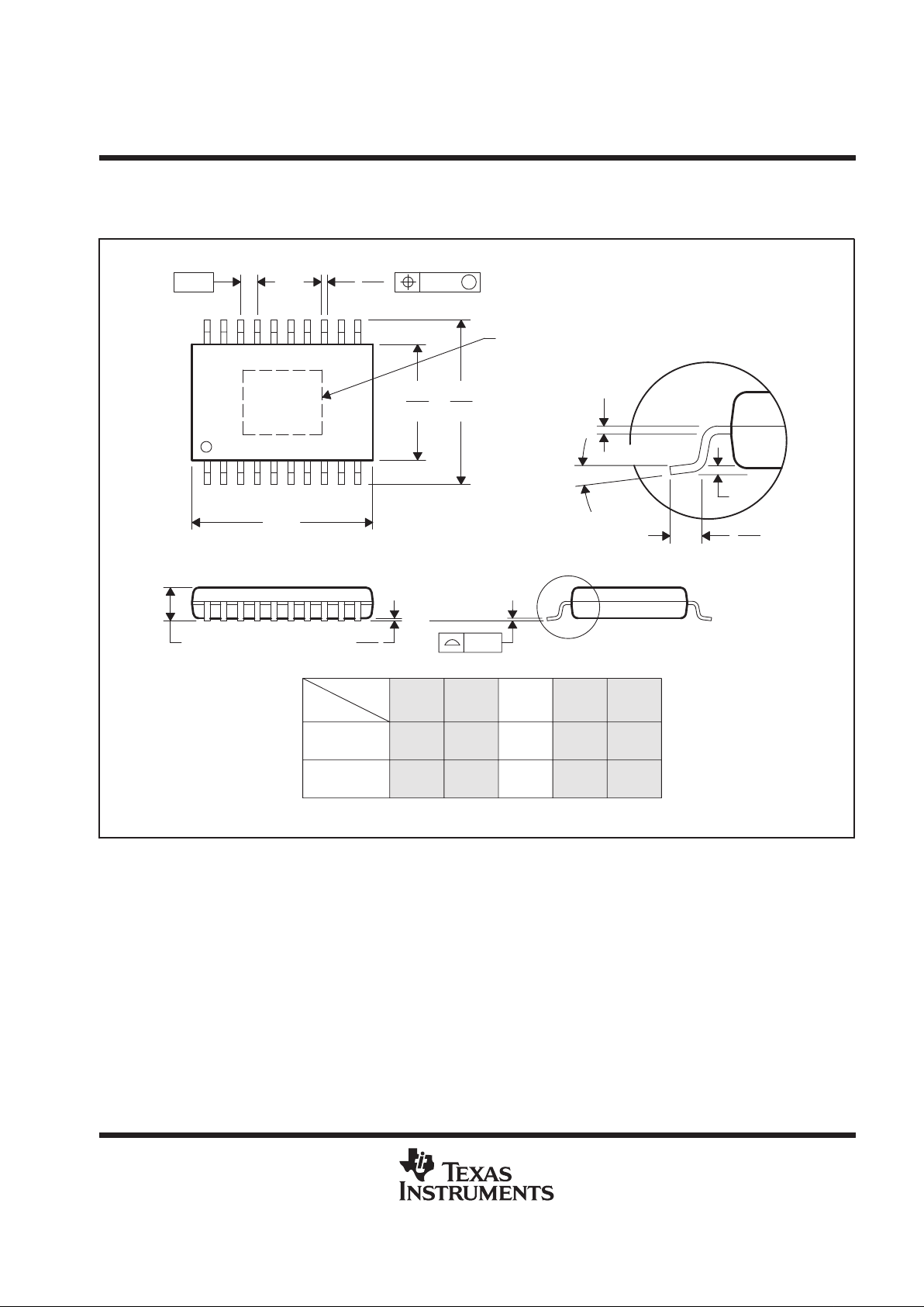
MECHANICAL DATA
PWP (R-PDSO-G**) PowerPAD PLASTIC SMALL-OUTLINE PACKAGE
4073225/E 03/97
0,50
0,75
0,25
0,15 NOM
Thermal Pad
(See Note D)
Gage Plane
2824
7,70
7,90
20
6,40
6,60
9,60
9,80
6,60
6,20
11
0,19
4,50
4,30
10
0,15
20
A
1
0,30
1,20 MAX
1614
5,10
4,90
PINS **
4,90
5,10
DIM
A MIN
A MAX
0,05
Seating Plane
0,65
0,10
M
0,10
0°–8°
20-PIN SHOWN
NOTES: A. All linear dimensions are in millimeters.
B. This drawing is subject to change without notice.
C. Body dimensions do not include mold flash or protrusions.
D. The package thermal performance may be enhanced by bonding the thermal pad to an external thermal plane. This pad is electrically
and thermally connected to the backside of the die and possibly selected leads.
E. Falls within JEDEC MO-153
PowerPAD is a trademark of Texas Instruments Incorporated.

IMPORTANT NOTICE
T exas Instruments and its subsidiaries (TI) reserve the right to make changes to their products or to discontinue
any product or service without notice, and advise customers to obtain the latest version of relevant information
to verify, before placing orders, that information being relied on is current and complete. All products are sold
subject to the terms and conditions of sale supplied at the time of order acknowledgment, including those
pertaining to warranty, patent infringement, and limitation of liability.
TI warrants performance of its semiconductor products to the specifications applicable at the time of sale in
accordance with TI’s standard warranty. Testing and other quality control techniques are utilized to the extent
TI deems necessary to support this warranty. Specific testing of all parameters of each device is not necessarily
performed, except those mandated by government requirements.
Customers are responsible for their applications using TI components.
In order to minimize risks associated with the customer’s applications, adequate design and operating
safeguards must be provided by the customer to minimize inherent or procedural hazards.
TI assumes no liability for applications assistance or customer product design. TI does not warrant or represent
that any license, either express or implied, is granted under any patent right, copyright, mask work right, or other
intellectual property right of TI covering or relating to any combination, machine, or process in which such
semiconductor products or services might be or are used. TI’s publication of information regarding any third
party’s products or services does not constitute TI’s approval, warranty or endorsement thereof.
Copyright 2000, Texas Instruments Incorporated
 Loading...