

Page 1
(6,4 mm x 7,8 mm)
www.ti.com
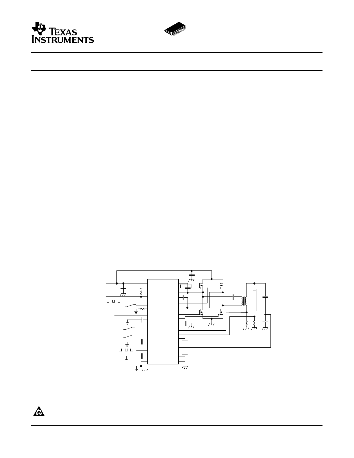
GA
GB
GC
GD
SA
PGND
SC
V5A
V5C
V5
CA−
CSEN
VA−
OCP
PH
SET
EN
VCC
VREF
GND
STC
ABR
BF
FAULT
VSEN
BBR
BC
C
1
Q
A
TPS68000
2 V
3.3 V
R
1
C
5
C
7
VLOGIC
Supply Voltage
8V .. 30V
Error Output
Operating Frequency
Device Enable
Lamp current
(Analog Dimming Input)
Burst Duty Cycle
(Burst Dimming Input)
Direct Burst Dimming Input
(Frequency + Duty Cycle)
C
10
C
3
C
4
C
2
C
12
C
13
R
4
R
3
C
8
C
9
SYNC
R
2
2.0 V
0 V
CAO
VAO
C
14
Q
C
Q
B
Q
D
T
1
C
6
0 V
0 V
Burst Frequency
Synchronization
Synchronization Phase Shift
SLVS524A – OCTOBER 2005 – REVISED FEBRUARY 2006
HIGHLY EFFICIENT PHASE SHIFT FULL BRIDGE CCFL CONTROLLER
FEATURES DESCRIPTION
• 8-V to 30-V Input Voltage Range
• Full Bridge Topology With Integrated Gate
Drives for 4 NMOS Switches
• Synchronizable Constant Frequency
Operation
• Programmable Phase Delays of Operating
Frequency for Master-Slave Operation
• Lamp Voltage and Lamp Current Regulation
• Analog and Burst Dimming
• Configurable Distributed Burst Dimming in
Multiple Controller Applications
• Programmable Voltage Regulation Timeout
for Startup and Fault Conditions
• Open-Lamp and Short-Circuit Protection
• Internal Over-Temperature Protection converter circuits driving multi-lamp applications,
• Undervoltage Lockout
• 30-pin TSSOP Package
APPLICATIONS
• CCFL Backlight Power Supplies for Desktop
Monitors and LCD TVs
• CCFL Backlight Power Supplies for Notebook
Computers
The TPS68000 device provides a power supply
controller solution for CCFL backlight applications in a
large variety of applications. The wide input voltage
range of 8 V to 30 V makes it suitable to be powered
directly from regulated 12-V or 24-V rails, or any
other source with output voltages in this range. When
using a 10% accurate regulated 5-V rail, it also can
be used in notebook computers or other portable
battery-powered equipment having lower minimum
supply voltages. The controller is capable of driving
the gates of all 4 NMOS switches directly without the
need for any additional circuitry, like dedicated gate
drivers or gate-drive transformers. The wide input
voltage range also makes it easy to design CCFL
converters with higher input voltages like 120 V or
400 V available at the output of a power factor
correction unit. The TPS68000 also supports CCFL
either by using higher power-rated switches and
transformers, or using several TPS68000s
synchronized. When synchronized, they can be
operated either at the same frequency and phase, or
phase shifted to minimize RMS input current. Already
implemented smart dimming features, such as
support of distributed dimming, also help to optimize
the performance of multi-controller applications.
(Continued on next page)
TPS68000
Distributed Dimming is a registered trademark of Texas Instruments.
PRODUCTION DATA information is current as of publication date.
Products conform to specifications per the terms of the Texas
Instruments standard warranty. Production processing does not
necessarily include testing of all parameters.
Please be aware that an important notice concerning availability, standard warranty, and use in critical applications of Texas
Instruments semiconductor products and disclaimers thereto appears at the end of this data sheet.
Copyright © 2005–2006, Texas Instruments Incorporated
Page 2

www.ti.com
TPS68000
SLVS524A – OCTOBER 2005 – REVISED FEBRUARY 2006
These devices have limited built-in ESD protection. The leads should be shorted together or the device placed in conductive foam
during storage or handling to prevent electrostatic damage to the MOS gates.
DESCRIPTION (CONTINUED)
To start the lamp, an automatic strike control is implemented. It smoothly increases the lamp voltage by
sweeping the operating frequency across the self resonance frequency of the transformer-series capacitor
resonant circuit. During this time the maximum lamp voltage is limited and regulated by a voltage control loop
until the lamp current increases to a value allowing the current control loop to take over control. The lamp current
is regulated over a wide current range. To set the lamp brightness, analog and PWM dimming circuits are
implemented. Analog and PWM dimming can be used independent of each other to control lamp brightness over
a wide range.
To protect the circuit during fault conditions, for example broken, disconnected, or shorted lamps, overvoltage
protection and overcurrent protection circuits are implemented. To protect the TPS68000 from overheating, an
internal temperature sensor is implemented that triggers controller turn-off at an excessive device temperature.
The device is packaged in a 30-pin TSSOP package measuring 6,4 mm x 7,8 mm (DBT).
AVAILABLE DEVICE OPTIONS
T
A
–40 ° C to 85 ° C 30-Pin TSSOP TPS68000DBT
(1) The DBT package is available taped and reeled. Add R suffix to device type (e.g., TPS68000DBTR) to order quantities of 2000 devices
per reel.
PACKAGE PART NUMBER
(1)
ABSOLUTE MAXIMUM RATINGS
over operating free-air temperature range (unless otherwise noted)
Input voltage range on VCC, EN, FAULT –0.3 V to 33 V
Input voltage range on SYNC, SET, PH, STC, ABR, BBR, BF, BC, VREF, VA-, VAO, CA-, CAO –0.3 V to 6 V
Input voltage range on VSEN, CSEN, OCP –6 V to 6 V
Input voltage range on GD, GB, V5 –0.3 V to 6 V
maximum differential voltage between GA, V5A and SA 6 V
maximum differential voltage between GC, V5C and SC 6 V
maximum differential voltage between SA and PGND 35 V
maximum differential voltage between SC and PGND 35 V
Operating virtual junction temperature range, T
Storage temperature range T
(1) Stresses beyond those listed under "absolute maximum ratings" may cause permanent damage to the device. These are stress ratings
only, and functional operation of the device at these or any other conditions beyond those indicated uner "recommended operating
conditions" is not implied. Exposure to absolute-maximum-rated conditions for extended periods may affect device reliability.
stg
J
(1)
TPS68000
–40 ° C to 150 ° C
–65 ° C to 150 ° C
DISSIPATION RATINGS
PACKAGE
DBT 63.9 ° C/W 1565 mW 16 mW/ ° C 860 mW 626 mW
THERMAL RESISTANCE POWER RATING DERATING FACTOR POWER RATING POWER RATING
θ
JA
TA≤ 25 ° C ABOVE TA= 25 ° C TA≤ 70 ° C TA≤ 85 ° C
RECOMMENDED OPERATING CONDITIONS
MIN NOM MAX UNIT
V
T
T
Supply voltage at VCC 8.0 30 V
I
Operating free air temperature range –40 85 ° C
A
Operating virtual junction temperature range –40 125 ° C
J
2
Submit Documentation Feedback
Page 3

www.ti.com
SLVS524A – OCTOBER 2005 – REVISED FEBRUARY 2006
ELECTRICAL CHARACTERISTICS
over recommended free-air temperature range and over recommended input voltage range (typical at an ambient temperature
range of 25 ° C) (unless otherwise noted)
PARAMETER TEST CONDITIONS MIN TYP MAX UNIT
MAIN CONTROL
V
5
I
OUT-V5
V
UVLO
V
OL
V
lkg
V
IL
V
IH
I
STC
I
STC
I
STC
V
REF
I
OUT-VREF
GATE DRIVE
MAIN OSCILLATOR
f 30 100 kHz
f
SYNC
V
IL
V
IH
I
SYNC
I
SYNC
Internal control supply regulator I
Control supply output current 25 mA
< 25 mA 4.5 5 5.5 V
OUT-V5
including internal current
consumption
Under voltage lockout threshold at V5 Voltage at V5 decreasing 4.0 4.1 4.3 V
FAULT output low voltage I
FAULT output leakage current V
= 500 µA 0.2 0.4 V
FAULT
= 5 V 0.1 1 µA
FAULT
EN input low voltage 0.4 V
EN input high voltage 1.4 V
EN input current V
= 24 V 0.05 0.1 µA
CC
STC source current during strike 6 µA
STC source current during wait 2 µA
STC source and sink current 10 µA
normal operation, V
1.25 V
=
STC
Overtemperature protection 140 ° C
Overtemperature hysteresis 20 ° C
Quiescent current into VCC VCC = 12 V, V5 = 5.5 V 30 50 µA
Quiescent current into VCC VCC = V5 = 5.5 V 25 40 µA
Quiescent current into V5 VCC = V5 = 5.5 V 1000 1500 µA
Shutdown current into VCC VCC = V5 = 5.5 V, EN = 0V 1 2 µA
Shutdown current into V5 VCC = V5 = 5.5 V, EN = 0V 1 2 µA
Shutdown current into VCC VCC = 12 V, EN = 0V 2.5 5 µA
Reference Voltage I
OUT-VREF
< 5 mA 3.27 3.3 3.33 V
Reference output current 5 mA
High side drive sink resistance ID= 0.05 A 1.2 2.0 Ω
High side drive source resistance ID= 0.05 A 1.5 2.5 Ω
High side drive rise time CG= 4.7 nF, SA= SC= 0 V, 35 50 ns
V
= V
5A
= 5 V
5C
High side drive fall time CG= 4.7 nF 15 25 ns
Time delay between high side off and CG= 4.7 nF 100 ns
low side on
Time delay between low side off and CG= 4.7 nF 100 ns
high side on
Low side drive sink resistance ID= 0.05 A 1.2 2.0 Ω
Low side drive source resistance ID= 0.05 A 1.5 2.5 Ω
Low side drive rise time CG= 4.7 nF, V5= 5 V 35 50 ns
Low side drive fall time CG= 4.7 nF 15 25 ns
Oscillator frequency programming
range
Frequency capture range for
synchronization
0.5 x f 2 x f
SYNC low voltage 0.4 V
SYNC high voltage 1.4 V
SYNC input current 0.5 1.5 µA
SYNC drive current V
VPH≤ V5- 1.3 V, V
V
≥ 1.4 V, V
SYNC
= 3.3
SYNC
= 5 V 1000 1250 1500 µA
PH
TPS68000
Submit Documentation Feedback
3
Page 4
www.ti.com
TPS68000
SLVS524A – OCTOBER 2005 – REVISED FEBRUARY 2006
ELECTRICAL CHARACTERISTICS (continued)
over recommended free-air temperature range and over recommended input voltage range (typical at an ambient temperature
range of 25 ° C) (unless otherwise noted)
PARAMETER TEST CONDITIONS MIN TYP MAX UNIT
I
SYNC
V
SET
I
PH
V
PH
VOLTAGE AND CURRENT CONTROL
R
CSEN
R
CSEN
R
VSEN
R
VSEN
I
, I
CAO
I
, I
CAO
VREF
VREF
VREF
I
OCP
I
OCP
VREF
DIMMING
I
ABR
V
ABR
I
BBR
V
BBR
I
BF
f
Burst
f
BC
t
r
I
BC
V
IL
V
IH
SYNC sink current V
Minimum pulse width for
synchronization
SYNC
≤ 0.4 V, V
= 5 V 1000 1250 1500 µA
PH
100 ns
SET output voltage 1.25 V
Phase shift of the main oscillator clock V
PH input current V
Threshold for programming device as
main oscillator frequency master
Current sense input impedance V
Current sense input impedance V
Voltage sense input impedance V
Voltage sense input impedance V
Voltage and current amplifier output
VAO
source current
Voltage and current amplifier output
VAO
sink current
Voltage regulator reference voltage (0.8 × V
VREG
Overvoltage comparator threshold V
OVP
Current regulator reference voltage V
CREG
Overcurrent comparator input current V
Overcurrent comparator input current V
Overcurrent comparator threshold V
OCP
ABR input current V
ABR input voltage range for lamp
current programming
BBR input current V
Burst duty cycle V
BBR input voltage threshold for
selecting synchronized burst dimming
= 0.1 V .. 1.9 V 90 ° / V
PH
= 2.0 V 0.1 1 µA
PH
V5– 1.3 V V5– 0.7 V V
= 3.3 V 35 k Ω
CSEN
= –3.3 V 25 k Ω
CSEN
= 3.3 V 25 k Ω
VSEN
= –3.3 V 30 k Ω
VSEN
V
, V
CAO
V
CAO
OCP
OCP
ABR
BC = V
BBR
BBR
= 2.5 V 55 µA
VAO
, V
= 2.5 V 200 µA
VAO
) / π V
REF
REF
ABR
= 3.3V 0.1 1 µA
= –3.3V 50 µA
REF
= 3.3 V 0.01 0.1 µA
5
0 3.3 V
= 2.0 V 0.1 1 µA
= 0 V .. 2 V 50 % / V
V5– 1.3 V V5– 0.7 V V
BF source current 10 µA
Internal burst frequency range 20 1000 Hz
Frequency lock / capture range for 0.5 x
synchronized burst dimming f
Burst
Burst current pulse rise time 400 µs
BC input current V
= 3.3V 0.1 1 µA
BC
BC input low voltage 0.4 V
BC input high voltage 1.4 V
minimum pulse width at BC 100 ns
Phase shift of the dimming burst V
compared to BC clock dimming selected
= 0 V .. 2 V, distributed
PH
180 ° / V
/ π V
1.5 x f
Burst
PH
V
V
BBR
PH
4
Submit Documentation Feedback
Page 5
www.ti.com
1
2
3
4
5
6
7
8
9
10
11
12
13
14
15
30
29
28
27
26
25
24
23
22
21
20
19
18
17
16
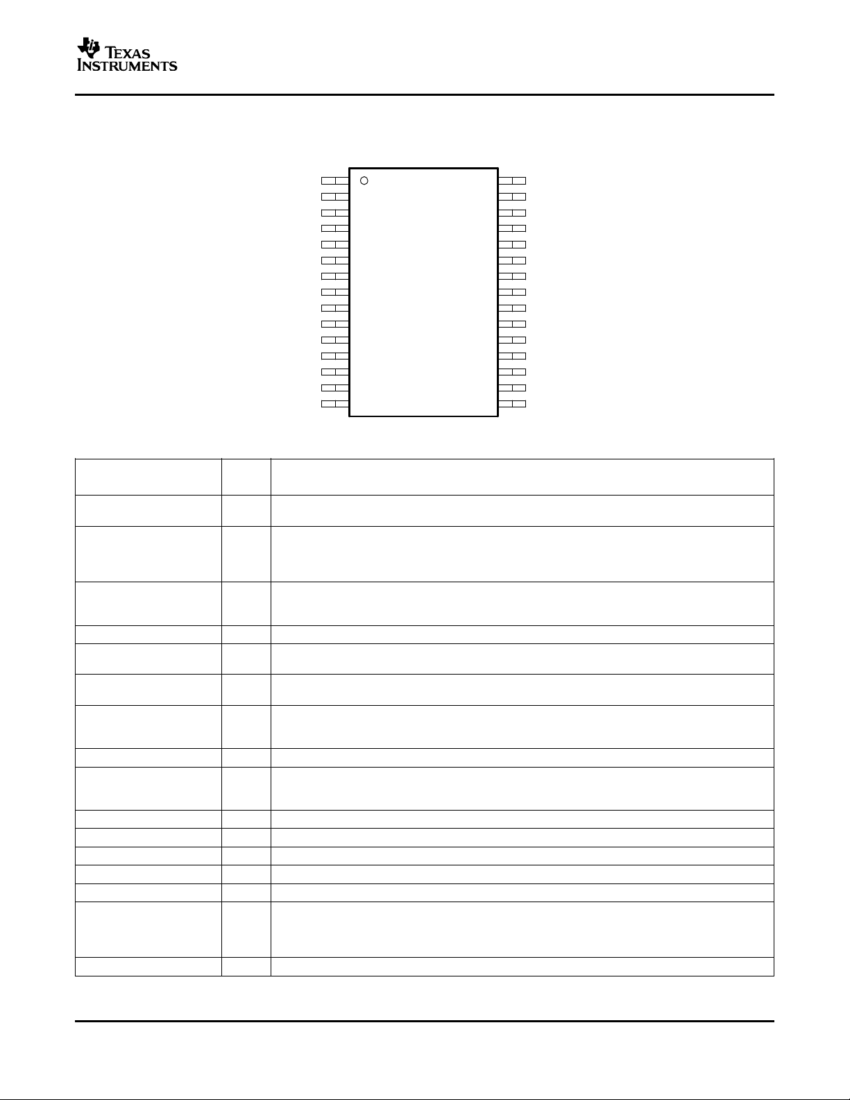
SYNC
SET
STC
PH
BBR
BC
BF
ABR
VAO
VA−
VSEN
CA−
CAO
CSEN
OCP
VREF
GND
SA
GA
V5A
GB
VCC
V5
PGND
GD
V5C
GC
SC
EN
FAULT
TPS68000
SLVS524A – OCTOBER 2005 – REVISED FEBRUARY 2006
PIN ASSIGNMENTS
DBT PACKAGE
(TOP VIEW)
Terminal Functions
TERMINAL
NAME NO.
ABR 8 I Analog brightness programming input. A DC voltage applied at that pin programs the lamp current
BBR 5 I Burst brightness programming input. A DC voltage applied at that pin programs the duty cycle of the
BC 6 I Burst control. A PWM signal applied at that pin is directly used for burst dimming. Frequency and
BF 7 I Burst frequency programming. A capacitor at that pin programs the burst frequency.
CA- 12 I Current amplifier negative input. This input is used to connect the compensation capacitor for
CAO 13 O Current amplifier output. This is the output for the current amplifier. It is used to connect the
CSEN 14 I Current sense. Measuring input for the lamp current. The applied voltage (coming from a shunt
EN 17 I Enable input. Logic high enables the device.
FAULT 16 O Error output, any detected malfunctioning of the application will be reported as error on this pin.
GA 27 O Gate drive output of switch A
GB 25 O Gate drive output of switch B
GC 19 O Gate drive output of switch C
GD 21 O Gate drive output of switch D
GND 29 Analog ground pin. Reference ground for all control signals.
OCP 15 I Over current protection. This input is used to monitor a voltage derived from a current sensor in any
PGND 22 Reference ground for the gate drivers and the gate drive supply.
I/O DESCRIPTION
the current regulator regulates. 0 V means no current and 3.3 V means maximum current.
burst pulses generated to dimm the brightness. 0 V means zero duty cycle and 2 V means
maximum duty cycle. Applying V5 (5 V) programs the device to operate in synchronized burst
dimming mode.
duty cycle are used directly. This input has priority against the burst frequency programming with
BBR and BF
compensating the current loop.
compensation capacitor for the current loop.
resistor) will be used for lamp current regulation. Sensed AC voltages can be applied directly. They
will be rectified internally.
Error means the output is pulled low. The output is open drain to allow connecting multiple error
outputs of similar devices together.
part of the converter. This voltage is compared to an internal reference voltage. Exceeding the
internal reference voltage causes the device logic to turn the device off and report an error signal at
the fault pin.
Submit Documentation Feedback
5
Page 6
www.ti.com
TPS68000
SLVS524A – OCTOBER 2005 – REVISED FEBRUARY 2006
PIN ASSIGNMENTS (continued)
Terminal Functions (continued)
TERMINAL
NAME NO.
PH 4 I Phase delay programming input. A voltage between 0 V and 2 V applied to that pin programs the
SA 28 Source connection of switch A
SC 18 Source connection of switch C
SET 2 I Operating frequency programming input. A resistor connected to this pin programs the internal
STC 3 I Startup capacitor. A capacitor connected to that pin determines the the time the device waits in
SYNC 1 I/O Synchronization input or operating frequency output. If the device is configured as master (see PH)
V5 23 I/O Input/Output of the internal 5 V regulator for gate drive supply and control supply. A capacitor must
V5A 26 O Supply input for the gate driver of the high-side switch A. A capacitor must be connected to that pin
V5C 20 O Supply input for the gate driver of the high side switch C. A capacitor must be connected to that pin
VA- 10 I Voltage amplifier negative input. This input is used to connect the compensation capacitor for
VAO 9 O Voltage amplifier output. This is the output for the voltage amplifier. It is used to connect the
VCC 24 I Device supply voltage input. VCC must be connected to V5 in case the device is powered directly
VREF 30 O Voltage reference. Output of the internal 3.3 V reference for use with all the analog control inputs.
VSEN 11 I Voltage sense. Measuring input for the lamp voltage. This voltage is used for lamp voltage
I/O DESCRIPTION
phase delay of the operating frequency compared to the synchronizing frequency. Applying V5 (5.0
V) programs the device as a master regarding the main oscillator frequency (see SYNC). The
voltage applied to that pin is also used to determine the phase delay in a distributed dimming
configuration
operating frequency.
voltage regulation for the lamp to strike.
the pin is used to provide the synchronization frequency for the slaves. Otherwise the device works
as slave and uses the applied frequency at that pin for synchronizing the operating frequency.
be connected to that pin to decouple switching noise caused by the gate drivers.
to supply the gate driver during switching (bootstrap).
to supply the gate driver during switching (bootstrap).
compensating the voltage loop.
compensation capacitor for the voltage loop.
from a regulated 5 V rail.
regulation (open lamp regulation) and overvoltage protection. Sensed AC voltages can be applied
directly. They are rectified internally.
6
Submit Documentation Feedback
Page 7
www.ti.com
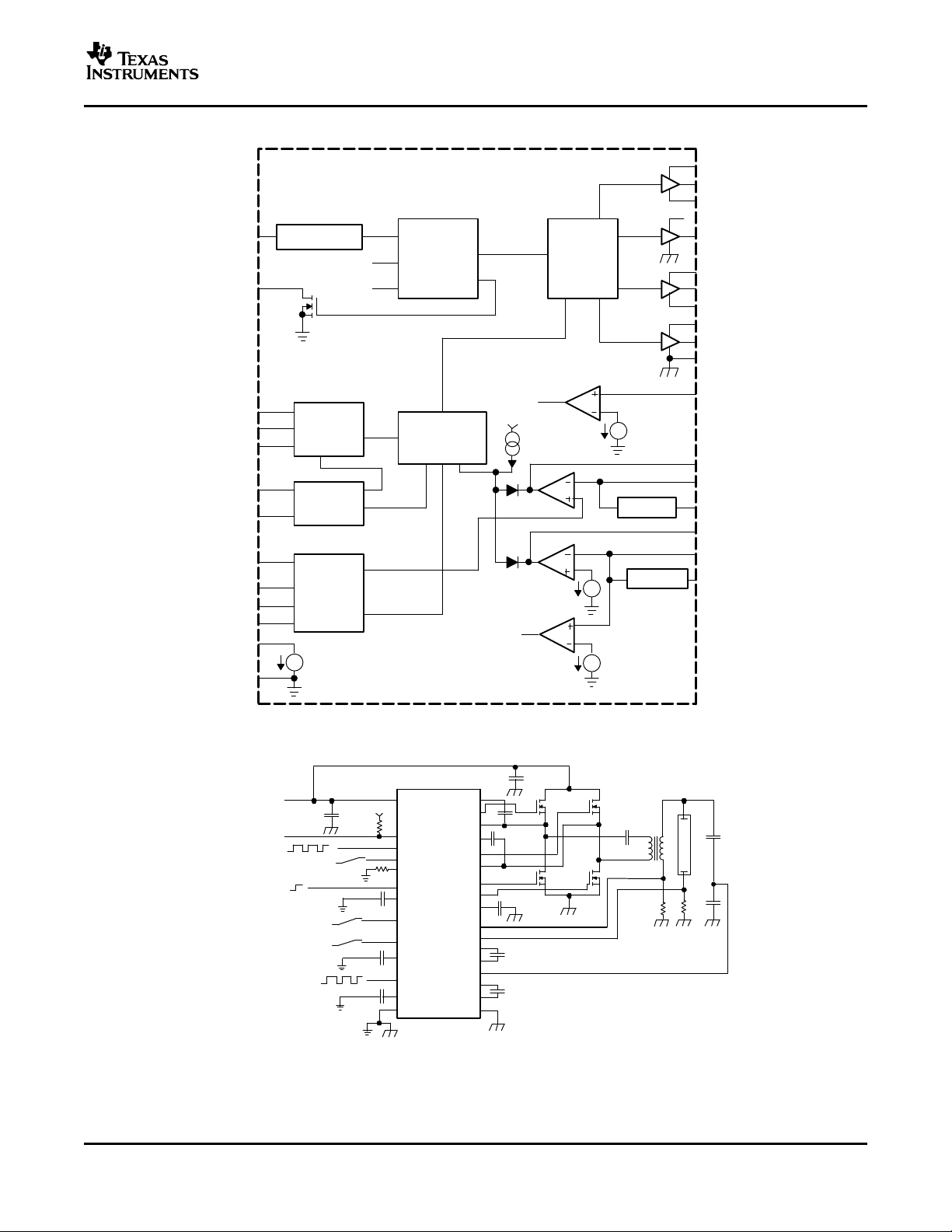
GA
GB
GC
GD
SA
PGND
SC
V5A
V5C
V5
Gate
Control
CA−
CAO
VA−
Main Control
VREF_OCP
OCP
Oscillator
Phase Shift
Control
SET
PH
EN
VCC
VREF
GND
Startup
and Strike
Control
STC
Analog
and
Burst
Dimming
ABR
BF
V5
VREF
VREF_VREG
VREF_OVP
OVP
V5
OVP
Control Supply
OCP
FAULT
OCP
VAO
OVP
BBR
BC
V5
VREF
Rectifier
CSEN
Rectifier
VSEN
SYNC
GA
GB
GC
GD
SA
PGND
SC
V5A
V5C
V5
CA−
CSEN
VA−
OCP
PH
SET
EN
VCC
VREF
GND
STC
ABR
BF
FAULT
VSEN
BBR
BC
C
1
Q
A
TPS68000
2 V
3.3 V
R
1
C
5
C
7
VLOGIC
Supply Voltage
8V .. 30V
Error Output
Operating Frequency
Device Enable
Lamp current
(Analog Dimming Input)
Burst Duty Cycle
(Burst Dimming Input)
Direct Burst Dimming Input
(Frequency + Duty Cycle)
C
10
C
3
C
4
C
2
C
12
C
13
R
4
R
3
C
8
C
9
SYNC
R
2
2.0 V
0 V
CAO
VAO
C
14
Q
C
Q
B
Q
D
T
1
C
6
0 V
0 V
Burst Frequency
Synchronization
Synchronization Phase Shift
FUNCTIONAL BLOCK DIAGRAM (TPS68000)
TPS68000
SLVS524A – OCTOBER 2005 – REVISED FEBRUARY 2006
PARAMETER MEASUREMENT INFORMATION
Submit Documentation Feedback
7
Page 8

www.ti.com
IO − Output Current at V5 − mA
4.5
4.6
4.7
4.8
4.9
5.0
5.1
5.2
5.3
5.4
5.5
0 10 20 30 40 50 60 70 80
VCC = 24 V
V
O
− Output Voltage at V5 − V
VCC = 12 V
IO − Output Current at VREF − mA
3.25
3.26
3.27
3.28
3.29
3.30
3.31
3.32
3.33
3.34
3.35
0 2 4 6 8 10 12 14 16
V
O
− Output Voltage at VREF − V
V5 = 5 V
TPS68000
SLVS524A – OCTOBER 2005 – REVISED FEBRUARY 2006
TYPICAL CHARACTERISTICS
Table of Graphs
Output voltage at V
Output voltage at V
5
REF
Operating frequency vs resistance at SET 3
Phase shift of operating frequency vs voltage at PH 4
Burst dimming duty cycle vs voltage at BBR 5
Burst dimming phase shift vs voltage at PH 6
Waveforms
vs output current at V
vs output current at V
Startup of V5 (V
Startup of V5 (V
Startup of V
REF
Lamp current and lamp voltage at startup (V
Lamp current and lamp voltage at startup (V
5
REF
= 12 V) 7
CC
= 24 V) 8
CC
(V
= V5 = 5V) 9
CC
= 12 V) 10
CC
= 24 V) 11
CC
Lamp current softstart at burst dimming 12
FIGURE
1
2
OUTPUT VOLTAGE AT V5 OUTPUT VOLTAGE AT V
vs vs
OUTPUT CURRENT AT V5 OUTPUT CURRENT at V
Figure 1. Figure 2.
REF
REF
8
Submit Documentation Feedback
Page 9

www.ti.com
Resistance at SET − kΩ
0
20
40
60
80
100
120
140
60 90 120 150 180 210 240 270 300 330 360
Operating Frequency − kHz
V5 = 5 V
Voltage at PH − V
0
20
40
60
80
100
120
140
160
180
0.0 0.2 0.4 0.6 0.8 1.0 1.2 1.4 1.6 1.8 2.0
Phase Shift of Operating Frequency − °
V5 = 5 V
Voltage at BBR − V
0
10
20
30
40
50
60
70
80
90
100
0.0 0.2 0.4 0.6 0.8 1.0 1.2 1.4 1.6 1.8 2.0
Burst Dimming Duty Cycle − %
V5 = 5 V
Voltage at PH − V
0
30
60
90
120
150
180
210
240
270
300
330
360
0.0 0.2 0.4 0.6 0.8 1.0 1.2 1.4 1.6 1.8 2.0
Burst Dimming Phase Shift − °
V5 = 5 V
TPS68000
SLVS524A – OCTOBER 2005 – REVISED FEBRUARY 2006
OPERATING FREQUENCY PHASE SHIFT OF OPERATING FREQUENCY
vs vs
RESISTANCE AT SET VOLTAGE AT PH
Figure 3. Figure 4.
BURST DIMMING DUTY CYCLE BURST DIMMING PHASE SHIFT
vs vs
VOLTAGE AT BBR VOLTAGE AT PH
Figure 5. Figure 6.
Submit Documentation Feedback
9
Page 10
www.ti.com
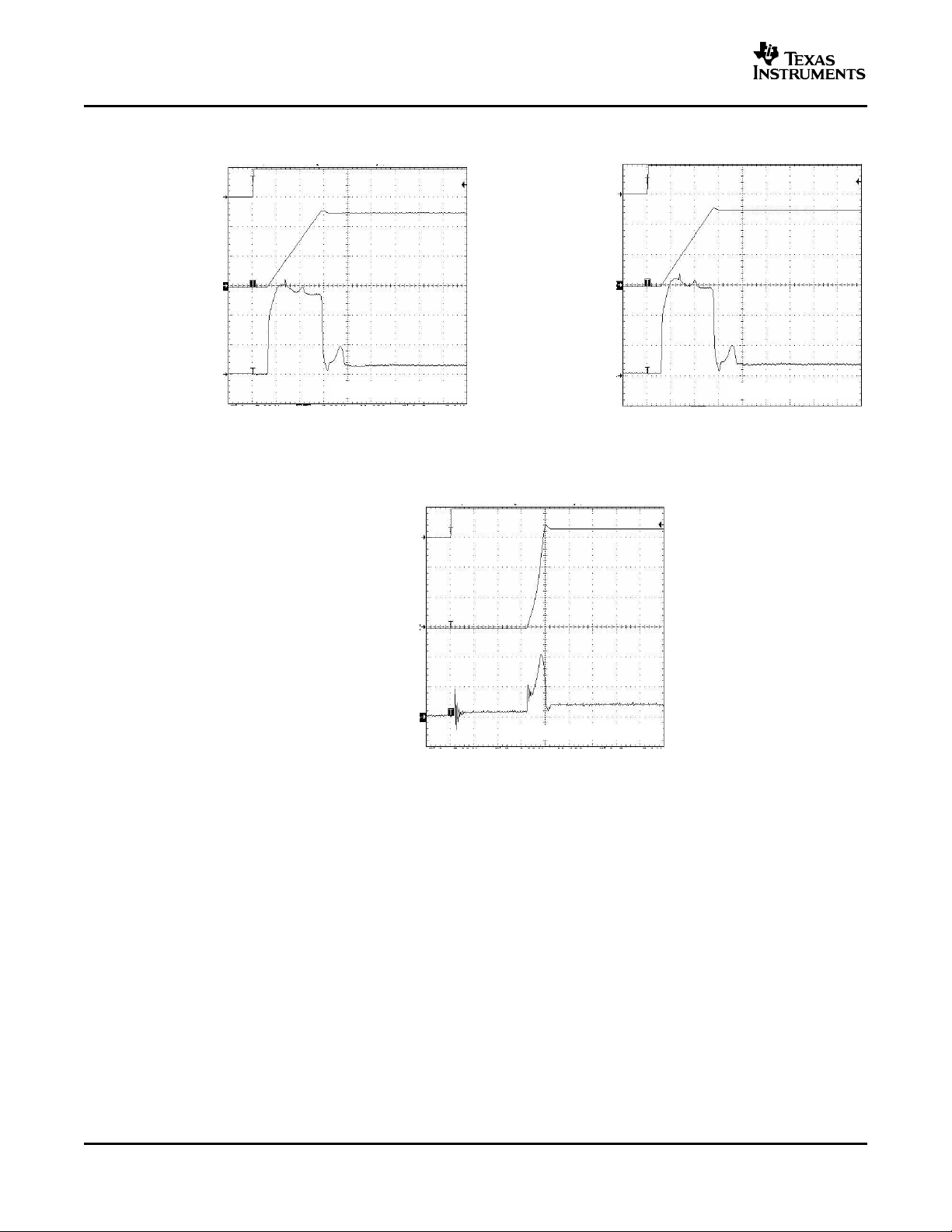
Timebase (100 µs /div)
VEN (5 V / div)
V5 (2 V / div)
Input Current (20 mA / div)
VCC = 12 V, IOUT_V5 = 5 mA
Timebase (100 µs /div)
VCC = 24 V, IOUT_V5 = 5 mA
VEN (5 V / div)
V5 (2 V / div)
Input Current (20 mA / div)
Timebase (100 µs /div)
VEN (5 V / div)
VREF (1 V / div)
Input Current (10 mA / div)
VCC = V5 = 5 V, IOUT_VREF = 2 mA
TPS68000
SLVS524A – OCTOBER 2005 – REVISED FEBRUARY 2006
STARTUP OF V5 STARTUP OF V5
VCC = 12 V VCC = 24 V
Figure 7. Figure 8.
STARTUP OF VREF
VCC = V5 = 5 V
10
Figure 9.
Submit Documentation Feedback
Page 11

www.ti.com
Timebase (200 ms /div)
Lamp Current (Voltage at CSEN) (5 V / div)
Lamp Voltage (Voltage at VSEN) (2 V / div)
VCC = 12 V
Timebase (200 ms /div)
Lamp Current (Voltage at CSEN) (5 V / div)
Lamp Voltage (Voltage at VSEN) (2 V / div)
VCC = 24 V
LAMP CURRENT AND
LAMP VOLTAGE AT STARTUP
TPS68000
SLVS524A – OCTOBER 2005 – REVISED FEBRUARY 2006
VCC = 12 V
Figure 10.
LAMP CURRENT AND
LAMP VOLTAGE AT STARTUP
VCC = 24V
Figure 11.
Submit Documentation Feedback
11
Page 12
www.ti.com
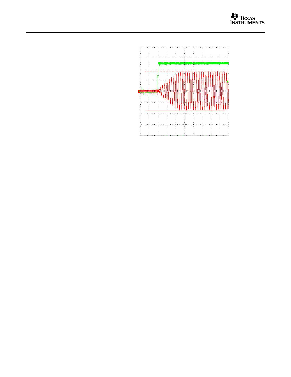
Timebase (100 µs /div)
Voltage at BC (2 V / div)
Lamp Current (Voltage at CSEN) (2 V / div)
VCC = 12 V
TPS68000
SLVS524A – OCTOBER 2005 – REVISED FEBRUARY 2006
LAMP CURRENT SOFTSTART
AT BURST DIMMING
Figure 12.
12
Submit Documentation Feedback
Page 13

www.ti.com
TPS68000
SLVS524A – OCTOBER 2005 – REVISED FEBRUARY 2006
DETAILED DESCRIPTION
Supply Voltages
The TPS68000 and the connected H-bridge power stage can be completely supplied by a voltage connected to
VCC. This voltage must be between 8 V to 30 V. In this configuration an internal linear regulator generates the 5
V required for control supply and gate drive supply. It is available at the V5 pin. The external capacitors for
supplying the high side gate drivers during operation are charged using internal diodes during the time when the
low side switches are turned on. The 3.3-V reference voltage is generated with a precise linear regulator, which
is also supplied from the 5-V control supply.
Optionally, the device can be supplied using a regulated 5-V rail. This is done by connecting the external 5 V to
VCC and V5. This way the internal regulator is bypassed and the internal power dissipation is reduced. It also
makes it possible to use any voltage lower than 30 V to supply the H-bridge power stage. When using
appropriate means of isolating the gate drive outputs of the device from their respective gates of the H-bridge
switches, the device can control power stages with higher input voltages as well. An example for this
configuration is using the output voltage of the PFC directly as a supply for the H-bridge power stage.
Gate Driver
The TPS68000 is a controller for converters, built with a full bridge topology. To control the output power
high-side and low-side switches in each of the two half bridges are driven alternately with 50% duty cycle. By
phase shifting both half-bridge parts to each other, output power is controlled. Current can only flow into the
transformer if one of the high side switches is turned on the same time as the low-side switch on the other
half-bridge is turned on. Maximum output power can be achieved if the turn on time of the high-side switch on
one half-bridge exactly overlaps with the turn on time of the low side on the other half bridge. Zero output power
will be if there is no overlap.
To properly control the 4 switches required for this phase shift full bridge topology, 4 gate drivers are
implemented. To obtain maximum efficiency at lowest costs the gate drivers are designed to drive 4 N-Channel
MOSFETs. The gate drive outputs can be connected directly to the gates of the FETs. There is no gate drive
circuit required as long as the operating input voltage range does not exceed the isolation voltage of the high
side drivers or the drive capability is not sufficient for larger FETs. The nominal gate drive voltage is 5 V. This
5-V rail is generated internally in the device and is used directly to supply the low side drivers. For the high side
drivers external capacitors are used to supply the drivers. They are charged up during the on time of the low-side
drivers.
Control Circuit
The device is able to control lamp current and lamp voltage directly. Lamp voltage and lamp current are sensed
with an appropriate feedback divider and a shunt resistor. By suitable designing feedback divider and shunt
resistor lamp current and maximum lamp voltage are programmed. Since the lamp needs to be operated with AC
current, the feedback signals in simple applications usually are AC voltages. To directly support this and to save
external components for rectification, internal half wave rectifiers are built in the device.
Regulating current and voltage is done by two independent error amplifiers. Both are compensated externally to
be flexible to meet the demands for a wide variety of CCFL backlight applications. Both error amplifier outputs
feed the phase shift modulator. Whichever error amplifier requires the lower duty cycle, takes over control of the
system. The control circuit also detects whether the device operates in voltage regulation or in current regulation.
If voltage regulation is detected a fault condition is assumed, for example a broken lamp. In this condition the
control circuit waits for a programmed wait time. If the current regulator does not take over control again during
this wait time, the device shuts down and sets the FAULT flag. The wait time is programmed with the size of the
capacitance at STC.
Protection
In addition to the voltage regulator other means of protection are implemented. To ensure that the secondary
voltage of the transformer does not exceed the isolation breakdown voltage of the transformer an overvoltage
comparator is implemented. This comparator monitors the rectified voltage at the VSEN input. If the peak voltage
level at VSEN rises 20% above the nominal regulation voltage, regulated by the voltage amplifier, the
overvoltage comparator trips and the device immediately enters FAULT condition. For detailed threshold values
please check the electrical characteristics table.
Submit Documentation Feedback
13
Page 14

www.ti.com
TPS68000
SLVS524A – OCTOBER 2005 – REVISED FEBRUARY 2006
DETAILED DESCRIPTION (continued)
For additional protection there is a standalone comparator implemented. It can be used to monitor any voltage in
the system. The switching threshold is set to the V
. This comparator monitors a voltage at its input and compares it with the internal reference voltage. As soon as
the input voltage of the comparator exceeds the reference voltage the comparator asserts FAULT at its output.
Negative voltages can be applied at that pin but there is no rectification. Since the input of the overcurrent
comparator is directly accessible at a pin it can be connected to any part of the circuit. It must not necessarily
use the shunt resistor used for current regulation. Monitoring the current in the secondary winding or any other
DC voltage in the system may be a desired approach as well.
Finally the device has an internal temperature sensor to monitor the IC temperature. If the temperature gets too
high FAULT is asserted as well. For detailed values for threshold and hysteresis of the thermal protection please
check the electrical characteristics table.
Oscillator
The device is operating at a fixed frequency which is generated by a built in PLL circuit. The frequency is
programmed with a resistor at SET. It also can be synchronized to an external frequency at SYNC. When
synchronizing to an external clock two modes are possible. One is to synchronize directly to the external clock,
the other is to synchronizeto the external clock but phase shifted. This helps to minimize the RMS input current
of the complete power converter application in a multi controller topology. This phase shift is programmed with a
DC voltage of 0 V to 2 V at PH for a phase shift of 0 ° to 180 ° .
voltage.
REF
Dimming
To dimm the lamp, two basic methods of dimming are supported. The first is to control the lamp current directly,
called analog dimming. The second is to turn the lamp on and off at a low frequency with a certain duty cycle,
called burst dimming. Analog dimming, is done by just providing a DC voltage at ABR. The lamp current will be
regulated propotional to that voltage. The maximum lamp current in burst dimming is also programmed with this
voltage at ABR.
Turning the lamp on and off, burst dimming, needs some more information. A low frequency must be generated
and duty cycle information for the on time needs to be provided. The simplest burst dimming mode, independent
burst dimming, is to program the low frequency with an external capacitor at BF. Applying a DC voltage at BBR
sets the duty cycle of the burst pulse. The burst duty cycle will be programmed proportional to the DC voltage at
BBR.
If the burst dimming frequency and duty cycle must be synchronized to an external PWM signal this external
signal can be connected to BC. The bursts follow the PWM signal directly. A PWM signal detected at BC has
priority to any internally generated burst signal. To force the device to take the BC PWM signal BBR can be tied
high (V5).
To minimize RMS input current in a multiple controller application the burst signal can be phase shifted to the
external PWM connected to BC, which is called Distributed Dimming
®
. Frequency and duty cycle stay the same.
The phase shift information is derived from the voltage at PH. Voltages of 0 V to 2 V at PH generate burst phase
shifts of 0 ° to 360 ° . For this mode of operation the internal low frequency oscillator is used. It is operated as a
PLL synchronized to the PWM frequency at BC and its center frequency has to be programmed at BF. The
compensation of the low frequency PLL is done with and R - C network connected at BBR.
Startup
When the device is enabled or the device is powered up with EN tied high, the device enters lamp strike mode.
In this mode no dimming and synchronization is possible. During the strike procedure the lamp current which
should flow when the lamp has turned on is programmed at ABR.
The device starts operating at double the programmed operating frequency and sweeps down to half of the
nominal frequency. During this sweep it can cross the self resonance frequency of the system with its maximum
voltage gain. As soon as the lamp current has reached its programmed value the device stops sweeping and
switches to the nominal operating frequency. The device will continue to regulate the lamp current and all other
control features like synchronization and burst dimming are enabled and will be used. If during this sweep the
14
Submit Documentation Feedback
Page 15

www.ti.com
TPS68000
SLVS524A – OCTOBER 2005 – REVISED FEBRUARY 2006
lamp voltage, which is programmed at the voltage regulator is reached, frequency sweeping is stopped and the
voltage regulator regulates the voltage at the programmed level. At that time a timer is started. If during this
waiting, the lamp current reaches its programmed value, the device will continue operating as described above. If
for any reason the timer reaches its programmed end, programmed by a capacitor at STC, the device stops
working and enters FAULT condition.
Submit Documentation Feedback
15
Page 16

www.ti.com
TPS68000
SLVS524A – OCTOBER 2005 – REVISED FEBRUARY 2006
APPLICATION INFORMATION
DESIGN PROCEDURE
This section describes the basic configuration and calculations which need to be done for getting the component
values necessary for configuring the device properly. Backlight inverters can be significantly more complex
especially when driving multiple lamps with one or more controllers. This will be described in seperate application
notes and documentation for reference designs and EVM's which are also available.
Decoupling and Filtering
For decoupling and filtering it is recommended to use capacitors with a low series resistance and inductance to
achieve optimum performance. Surface mount ceramic capacitors are a good choice. It is also recommended to
use short and wide traces to connect those decoupling capacitors to the controller.
For the high side gate drivers in typical applications at least a 1- µ F supply capacitor is recommended. It should
be connected between SA to V5A and SC to V5C with connectio placed as close as possible to the respective
pins to make sure that the gate drive outputs have a low impedance power source.
The V5 control supply requires a decoupling capacitor as well. It should be similar in capacitance as used for
both of the high side gate drivers. Example if a typical 1uF capacitor is used at the high side drivers therefore 2.2
µ F is recommended at V5.
If V5 is used as an input, which means the controller is supplied with regulated 5 V directly, V5 must be
connected to VCC to avoid reverse current flowing and malfunctioning of the control circuits directly powered
from VCC.
In case the V5 regulator is supplied via the VCC input it is recommended to use a decoupling capacitor at the
VCC pin. The capacitor should be at least 0.1 µ F. For additional filtering a resistor in series can be used.
For all those capacitors the PGND pin at the IC should be the reference ground.
Connecting the Gates of the MOSFETs
The gates of the MOSFETs of the power stage should be connected with short and wide traces having a low
impedance. The respective ground connection should be similar in width and length. Special care should be
taken on the loop area formed by the gate drive trace and the respective ground return trace, that it is as small
as possible. Any vias in this traces should be avoided.
If there is a need to slow down the switching speed of the FETs to reduce EMI caused by switching transients,
gate resistors at the gate drive outputs can be used.
Voltage Reference
The internal reference voltage is available at the VREF pin. It is recommended to decouple it at this pin using a
minimum 0.22 µ F capacitor to the analog ground reference pin GND. Short direct connections are
recommended.
Enabling the Controller
A logic high at the EN pin enables the controller. The enable thresholds are designed to meet requirements of
3.3 V and 1.8 V logic standards. Nevertheless it is also possible to connect EN directly to VCC to enable the
controller at power up, since the EN pin can withstand voltages as high as allowed at VCC.
If the device detects a fault it is automatically disabled. To allow the device to automatically restart after a fault,
FAULT and EN pins can be directly connected together using a common pull up resistor to VCC.
Fault Output
The fault output is open drain. It is low impedance to GND if the controller detected a fault. In normal operation it
is always high impedance. To make sure that a logic low at the FAULT pin has a lower voltage than 0.4 V the
pullup resistor should limit the current into the FAULT pin to a value lower than 0.5 mA. Equation 1 shows the
calculation:
16
Submit Documentation Feedback
Page 17

www.ti.com
R
FAULT
V
LOGIC
0.5 mA
R
SET
9720 k kHz
f
N
N
VPH 90
o
V
tSW C
STC
0.42
s
F
TPS68000
SLVS524A – OCTOBER 2005 – REVISED FEBRUARY 2006
APPLICATION INFORMATION (continued)
R
connected to FAULT.
Main Oscillator
In normal operation the controller operates at the frequency of the main oscillator. It is programmed with a
resistor connecting the SET pin to GND. The resistor value is calculated using Equation 2 :
If the controller should be synchronized to an external clock the main oscillator frequency should be programmed
close to the synchronizing frequency. This avoids large variations in case external clock pulses are missing. It
also speeds up the locking to the external clock. The SET pin should never be left open.
Synchronization of the Main Oscillator
The main oscillator can be used in different modes of operation. The first and most important mode is using it as
a reference clock. This is also the mode of choice in a single controller application which is not synchronized to
an external clock. In this mode the SYNC pin is used as an output and should be left open if no circuit needs to
be synchronized to the device main oscillator clock. To force the device operating in this mode 5 V (V5) must be
connected to the PH pin.
Lower voltages applied at the PH pin configure the SYNC pin as an input. Detailed voltage levels for this can be
found in the electrical characteristics table. If the SYNC pin is configured as an input the device automatically
synchronizes the main oscillator to the frequency which must be applied at the SYNC pin. The compensation for
this main oscilator PLL circuit is done with a capacitor connected at the STC pin. Since this capacitor is used for
defining sweep and wait timing during startup and voltage regulation, synchronization is only possible when the
device has started and is regulating lamp current. Any capacitance value which makes sense for defining sweep
and wait time should offer a reasonable compensation for the main oscillator PLL. How to calculate the value for
the capacitor at STC to program the startup and wait timing is shown in the following paragraph. Typical values
are in a µ F range.
Also a phase shifted synchronization can be programmed. For this a voltage in the range between 0 V and 2 V
must be applied at the PH pin. For calculating the phase shift of the main oscillator clock to the clock applied at
the SYNC pin Equation 3 can be used:
is the minimum resistance value of the pullup resistor, V
FAULT
is the maximum supply voltage of the logic
LOGIC
(1)
(2)
In this equation φNis the main oscillator clock phase shift and V
is the voltage applied at the PH pin.
PH
Startup and Wait Timing
After enabling the device the device is starting at double the programmed main oscillator frequency and is
sweeping down to half the programmed main oscillator frequency. The timing for the sweep is programmed with
a capacitor connected between STC and GND. It can be calculated using Equation 4 :
tSWis the sweep time and C
If at any time the voltage regulator becomes active a wait timer is started. The timing is also programmed with a
capacitor connecting STC and GND. Open lamp condition will lead to shutdown after timeout. Equation 5 shows
how to calculate the wait time, tW:
is the capacitance connected between the pins STC and GND.
STC
Submit Documentation Feedback
(3)
(4)
17
Page 18

www.ti.com
tW C
STC
0.63
s
F
R
Shunt
V
ABR
I
Lamp
2
R
Shunt
3.3 V
I
Lamp
2
I
Lamp
V
ABR
R
Shunt
2
r
V
V
REG
1.87 V
V
OVP
2.33 V r
V
TPS68000
SLVS524A – OCTOBER 2005 – REVISED FEBRUARY 2006
APPLICATION INFORMATION (continued)
Programming the Lamp Current
The lamp current which is an AC signal is sensed at the CSEN input. The AC signal is half-wave rectified
through internal circuits eliminating the need for external parts except for a current sense resistor. The error
amplifier will generate an average voltage from the half wave rectified input signal. This average voltage is
compared to the steering signal for the lamp current. This steering signal is always provided at the ABR input. It
is recommended to use the reference voltage as a maximum input voltage. For a sinusoidal feedback voltage at
CSEN the peak voltage matches the voltage applied at ABR. With this information the shunt resistor for a given
RMS lamp current can be calculated using Equation 6 :
Assuming that the reference voltage is connected to ABR the lamp current is calculated as shown in the
following Equation 7 :
R
is the value of the shunt resistor used for current sensing, V
Shunt
the RMS value of the lamp current which should be programmed.
is the voltage applied at ABR and I
ABR
Lamp
(5)
(6)
(7)
is
Analog Dimming
By modifiying the voltage at ABR the lamp current steering signal is changed. With this the lamp current is
changed. The resulting lamp current for a certain voltage at ABR can be calculated as shown in Equation 8 :
I
is the RMS lamp current, V
Lamp
is the voltage at ABR and R
ABR
is the value of the resistor used for lamp
Shunt
current sensing.
Programming the Voltage Regulation and Overvoltage Protection
The lamp voltage and the transformer secondary voltage are AC signals as is the lamp current. They are sensed
at the VSEN input. Circuits similar to the current amplifier (CSEN) half wave rectified input are eliminating the
requirement for rectification on VSEN. The error amplifier will generate an average voltage from the half wave
rectified input signal. This average voltage is compared to the steering signal for the voltage. This steering signal
is derived from the internal reference voltage V
VSEN. Its threshold is the internal reference voltage. The voltage divider ratio can be calculated using
Equation 9 :
rVis the ratio of the voltage feedback divider and V
regulate at the lamp or transformer secondary.
The corresponding RMS voltage where the overvoltage protection comparator turns off can be calculated using
Equation 10 :
. The overvoltage comparator is monitoring the peak voltage at
REF
is the maximum RMS voltage the regulator should
REG
(8)
(9)
To build the voltage feedback divider, resistive and capacitive dividers can be used. In case of a resistive divider
the ratio of the feedback divider is defined as shown in Equation 11 :
18
Submit Documentation Feedback
(10)
Page 19

www.ti.com
r
V
RH R
L
R
L
r
V
CH C
L
C
H
C
BF
4.7
f
D
F Hz
DB V
BBR
50
%
V
TPS68000
SLVS524A – OCTOBER 2005 – REVISED FEBRUARY 2006
APPLICATION INFORMATION (continued)
R
is the upper resistor in the divider at the high voltage side, R
H
In case of a capacitive divider the ratio can be calculated as shown in Equation 12 :
In this case C
is the upper capacitor in the divider at the high voltage side, C
H
Protection
The overcurrent protection comparator (OCP) is typically used to monitor output current but can be configured to
monitor any voltage. The comparator uses the internal reference voltage V
above the internal reference voltage at OCP for more than 4 clock cycles of the main oscillator causes the
comparator to trip and generate a fault. The comparator only will trip with positive voltages above the internal
reference voltage at applied to OCP. Although the input can withstand higher negative voltages there is no
rectification implemented.
Compensating the Current and Voltage Regulators
The compensation networks for current and voltage regulators are connected between the negative inputs and
the outputs of the respecive amplifier. At the current amplifier the pins are CAM (input) and CAO (output). At the
voltage amplifier VAM (input) and VAO (output) are used. The compensation network must have a dominating
capacitive characteristic, since the error amplifiers are also used for smoothing the half wave rectified feedback
input signal. capacitors in parallel with resistor and capacitor in series or just capacitors are recommended. In
typical applications a 2200 pF capacitor at the current amplifier and a 0.022 µ F capacitor at the voltage amplifier
can be used.
is the resistor to GND.
L
is the capacitor to GND.
L
as a fixed threshold. Any voltage
REF
(11)
(12)
Synchronized Burst Dimming
To configure the device for synchronized burst dimming the dimming PWM signal must be connected directly to
the BC logic input pin. The controller will turn the lamp on and off, following directly the PWM pulses applied at
BC regarding frequency, phase and duty cycle. The slopes of the lamp current are controlled internally. The other
pins used for configuring burst dimming, BBR and BF should have a defined state as well. It is recommended to
connect BBR to 5 V (V5) and to connect BF to GND.
Independent Burst Dimming
In this configuration the device generates the low dimming frequency and the duty cycle internally. To use this
feature the BC pin should be connected to GND. A capacitor connected to BF is used to program the frequency
of the low frequency oscillator. The capacitance necessary to program a given burst dimming frequency can be
calculated using Equation 13 :
C
is the capacitor required to be connected between BF and GND and fDis the low frequency oscillator
BF
frequency which should be programmed. For example a 0.047 µ F capacitor is needed to program a burst
frequency of 100 Hz.
To program the burst duty cycle a voltage at BBR is used. The duty cycle can be calculated using Equation 14 :
D
is the resulting burst duty cycle and V
B
for duty cycle programming is 0 V to 2 V. 0 V at BBR will program 0% burst duty cycle and 2 V will program
100% burst duty cycle.
is the voltage applied at the BBR pin. The operating voltage range
BBR
(13)
(14)
Submit Documentation Feedback
19
Page 20

www.ti.com
B
VPH 180
o
V
P
D(MAX)
T
J(MAX)
T
A
R
JA
125oC 85oC
63.9
o
C
W
626 mW
TPS68000
SLVS524A – OCTOBER 2005 – REVISED FEBRUARY 2006
APPLICATION INFORMATION (continued)
Phase Shifted Burst Dimming
The device also supports phase shifted burst dimming. In this configuration a direct PWM burst signal is used
which must be connected to BC. The internal low frequency oscillator must be programmed as described in the
independent burst dimming section and in Equation 13 . Since the internal low frequency oscillator will be
synchronized to the frequency connected to BC it is recommended to program the internal low frequency close to
the frequency at BC. The synchronization is done using a PLL circuit. This PLL circuit needs an external
compensation network connected at BBR. For a typical burst frequency in the 100 Hz range using a 0.68 µ F
capacitor in series with a 100 k Ω resistor is recommended. This R - C network should be connected between
BBR and GND.
The phase shift of the dimming burst compared to the input signal at BC is programmed with a voltage applied at
PH. The resulting phase shift can be calculated using Equation 15 :
φBis the phase shift of the dimming burst and V
Layout Considerations
As for all switching power supplies, the layout is an important step in the design, especially at high peak currents
and high switching frequencies. If the layout is not carefully done, the regulator could show stability problems as
well as EMI problems. Therefore, use wide and short traces for the main current path and for the power ground
tracks. Use a common ground node for power ground and a different one for control ground to minimize the
effects of ground noise. Connect these ground nodes at any place close to one of the ground pins of the IC.
To layout the control ground, it is recommended to use short traces as well, separated from the power ground
traces. This avoids ground shift problems, which can occur due to superimposition of power ground current and
control ground current.
is the voltage applied at the PH pin.
PH
(15)
THERMAL INFORMATION
Implementation of integrated circuits in low-profile and fine-pitch surface-mount packages typically requires
special attention to power dissipation. Many system-dependent issues such as thermal coupling, airflow, added
heat sinks and convection surfaces, and the presence of other heat-generating components affect the
power-dissipation limits of a given component.
Three basic approaches for enhancing thermal performance are listed below.
• Improving the power dissipation capability of the PCB design
• Improving the thermal coupling of the component to the PCB
• Introducing airflow in the system
The maximum recommended junction temperature (T
of the 30-pin TSSOP package (PW) is R
ambient temperature T
of 85° C. Therefore, the maximum power dissipation is about 626 mW. More power can
A
= 63.9° C/W. Specified regulator operation is assured to a maximum
θ JA
be dissipated if the maximum ambient temperature of the application is lower.
) of the TPS68000 device is 125° C. The thermal resistance
J
(16)
20
Submit Documentation Feedback
Page 21

PACKAGE OPTION ADDENDUM
www.ti.com
18-Jul-2006
PACKAGING INFORMATION
Orderable Device Status
(1)
Package
Type
Package
Drawing
Pins Package
Qty
Eco Plan
TPS68000DBT ACTIVE SM8 DBT 30 60 Green (RoHS &
no Sb/Br)
TPS68000DBTG4 ACTIVE SM8 DBT 30 60 Green (RoHS &
no Sb/Br)
TPS68000DBTR ACTIVE SM8 DBT 30 2000 Green (RoHS &
no Sb/Br)
TPS68000DBTRG4 ACTIVE SM8 DBT 30 2000 Green (RoHS &
no Sb/Br)
(1)
The marketing status values are defined as follows:
ACTIVE: Product device recommended for new designs.
LIFEBUY: TI has announced that the device will be discontinued, and a lifetime-buy period is in effect.
NRND: Not recommended for new designs. Device is in production to support existing customers, but TI does not recommend using this part in
a new design.
PREVIEW: Device has been announced but is not in production. Samples may or may not be available.
OBSOLETE: TI has discontinued the production of the device.
(2)
Eco Plan - The planned eco-friendly classification: Pb-Free (RoHS), Pb-Free (RoHS Exempt), or Green (RoHS & no Sb/Br) - please check
http://www.ti.com/productcontent for the latest availability information and additional product content details.
TBD: The Pb-Free/Green conversion plan has not been defined.
Pb-Free (RoHS): TI's terms "Lead-Free" or "Pb-Free" mean semiconductor products that are compatible with the current RoHS requirements
for all 6 substances, including the requirement that lead not exceed 0.1% by weight in homogeneous materials. Where designed to be soldered
at high temperatures, TI Pb-Free products are suitable for use in specified lead-free processes.
Pb-Free (RoHS Exempt): This component has a RoHS exemption for either 1) lead-based flip-chip solder bumps used between the die and
package, or 2) lead-based die adhesive used between the die and leadframe. The component is otherwise considered Pb-Free (RoHS
compatible) as defined above.
Green (RoHS & no Sb/Br): TI defines "Green" to mean Pb-Free (RoHS compatible), and free of Bromine (Br) and Antimony (Sb) based flame
retardants (Br or Sb do not exceed 0.1% by weight in homogeneous material)
(2)
Lead/Ball Finish MSL Peak Temp
CU NIPDAU Level-2-260C-1 YEAR
CU NIPDAU Level-2-260C-1 YEAR
CU NIPDAU Level-2-260C-1 YEAR
CU NIPDAU Level-2-260C-1 YEAR
(3)
(3)
MSL, Peak Temp. -- The Moisture Sensitivity Level rating according to the JEDEC industry standard classifications, and peak solder
temperature.
Important Information and Disclaimer:The information provided on this page represents TI's knowledge and belief as of the date that it is
provided. TI bases its knowledge and belief on information provided by third parties, and makes no representation or warranty as to the
accuracy of such information. Efforts are underway to better integrate information from third parties. TI has taken and continues to take
reasonable steps to provide representative and accurate information but may not have conducted destructive testing or chemical analysis on
incoming materials and chemicals. TI and TI suppliers consider certain information to be proprietary, and thus CAS numbers and other limited
information may not be available for release.
In no event shall TI's liability arising out of such information exceed the total purchase price of the TI part(s) at issue in this document sold by TI
to Customer on an annual basis.
Addendum-Page 1
Page 22
Page 23

IMPORTANT NOTICE
Texas Instruments Incorporated and its subsidiaries (TI) reserve the right to make corrections, modifications,
enhancements, improvements, and other changes to its products and services at any time and to discontinue
any product or service without notice. Customers should obtain the latest relevant information before placing
orders and should verify that such information is current and complete. All products are sold subject to TI’s terms
and conditions of sale supplied at the time of order acknowledgment.
TI warrants performance of its hardware products to the specifications applicable at the time of sale in
accordance with TI’s standard warranty. Testing and other quality control techniques are used to the extent TI
deems necessary to support this warranty . Except where mandated by government requirements, testing of all
parameters of each product is not necessarily performed.
TI assumes no liability for applications assistance or customer product design. Customers are responsible for
their products and applications using TI components. To minimize the risks associated with customer products
and applications, customers should provide adequate design and operating safeguards.
TI does not warrant or represent that any license, either express or implied, is granted under any TI patent right,
copyright, mask work right, or other TI intellectual property right relating to any combination, machine, or process
in which TI products or services are used. Information published by TI regarding third-party products or services
does not constitute a license from TI to use such products or services or a warranty or endorsement thereof.
Use of such information may require a license from a third party under the patents or other intellectual property
of the third party, or a license from TI under the patents or other intellectual property of TI.
Reproduction of information in TI data books or data sheets is permissible only if reproduction is without
alteration and is accompanied by all associated warranties, conditions, limitations, and notices. Reproduction
of this information with alteration is an unfair and deceptive business practice. TI is not responsible or liable for
such altered documentation.
Resale of TI products or services with statements different from or beyond the parameters stated by TI for that
product or service voids all express and any implied warranties for the associated TI product or service and
is an unfair and deceptive business practice. TI is not responsible or liable for any such statements.
Following are URLs where you can obtain information on other Texas Instruments products and application
solutions:
Products Applications
Amplifiers amplifier.ti.com Audio www.ti.com/audio
Data Converters dataconverter.ti.com Automotive www.ti.com/automotive
DSP dsp.ti.com Broadband www.ti.com/broadband
Interface interface.ti.com Digital Control www.ti.com/digitalcontrol
Logic logic.ti.com Military www.ti.com/military
Power Mgmt power.ti.com Optical Networking www.ti.com/opticalnetwork
Microcontrollers microcontroller.ti.com Security www.ti.com/security
Low Power Wireless www.ti.com/lpw Telephony www.ti.com/telephony
Video & Imaging www.ti.com/video
Wireless www.ti.com/wireless
Mailing Address: Texas Instruments
Post Office Box 655303 Dallas, Texas 75265
Copyright 2006, Texas Instruments Incorporated
 Loading...