

Texas Instruments TPS6734IP, TPS6734IDR, TPS6734ID, TPS6734EVM Datasheet
Please be aware that an important notice concerning availability, standard warranty, and use in critical applications of
Texas Instruments semiconductor products and disclaimers thereto appears at the end of this data sheet.
TPS6734I
FIXED 12-V 120-mA BOOST-CONVERTER SUPPLY
SLVS127A – AUGUST 1995 – REVISED JANUAR Y 1999
1
POST OFFICE BOX 655303 • DALLAS, TEXAS 75265
D
Pin-for-Pin Compatible With MAX734
D
Programming Voltage for Flash Memory
D
2.7-V to 11-V Input Operating Range
D
Output Current of 120 mA or Greater From
3.75-V or Higher Input
D
3-µA Maximum Supply Current in
Shutdown
D
Only 5 External Components Required
D
High Efficiency...85% Typical (5-V Input,
120-mA Output)
D
8-Pin SOIC and DIP Packages
D
–40°C to 85°C Free-Air Operating
T emperature Range
description
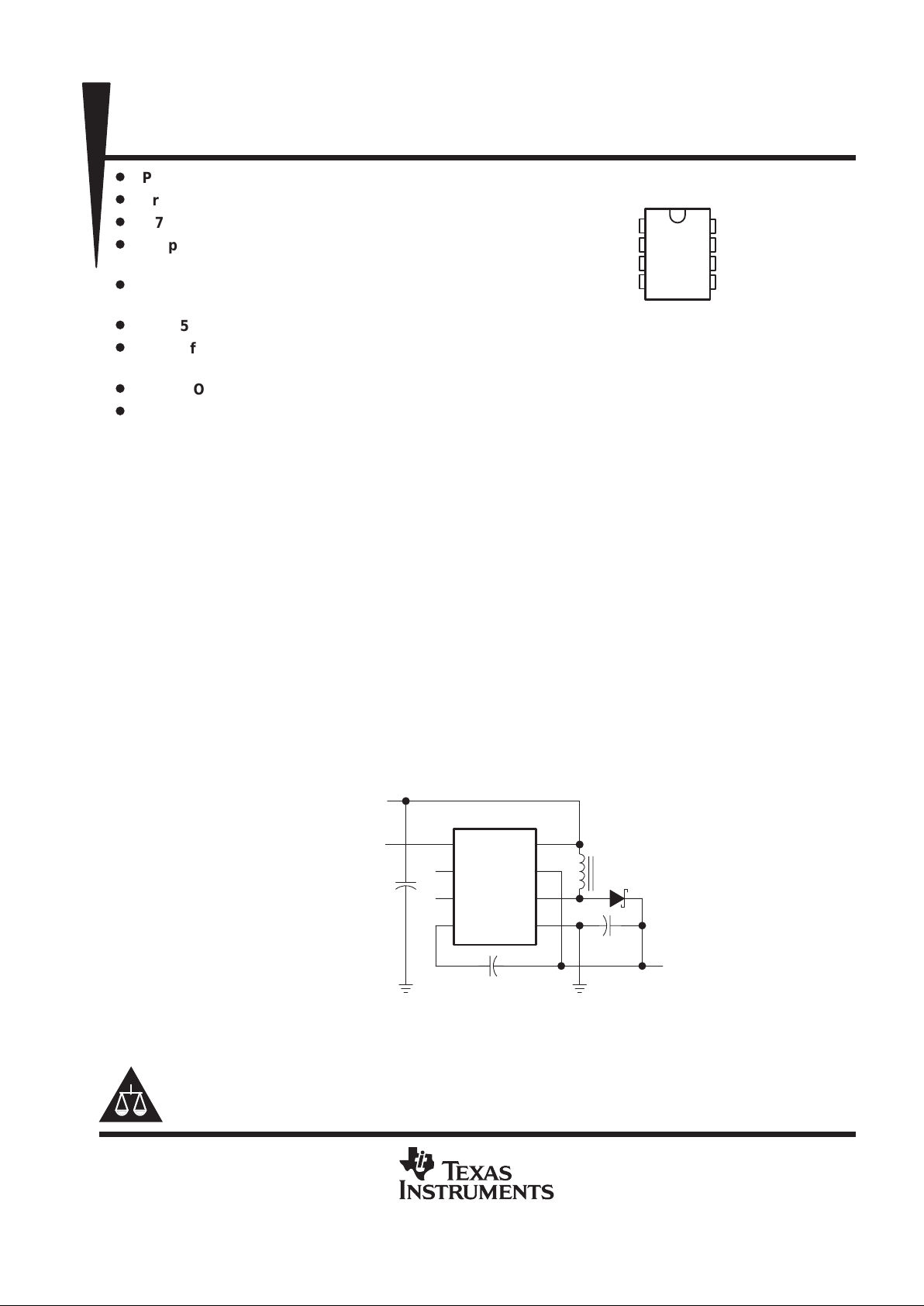
The TPS6734 is a fixed 12-V output boost converter capable of delivering 120 mA from inputs as low as
3.75 V. The device is pin-for-pin compatible with the MAX734 regulator and offers the following advantages:
lower supply current, wider operating input-voltage range, and higher output currents. As shown in Figure 1,
the only external components required are: an inductor, a Schottky rectifier, an output filter capacitor, an input
filter capacitor, and a small capacitor for loop compensation. The entire converter occupies less than 0.7 in
2
of
PCB space when implemented with surface-mount components. An enable input is provided to shut down the
converter and reduce the supply current to 3 µA when 12 V is not needed.
The TPS6734 is a 170-kHz current-mode PWM ( pulse-width modulation) controller with an n-channel MOSFET
power switch. Gate drive for the switch is derived from the 12-V output after start-up to minimize the die area
needed to realize the 0.7-Ω MOSFET and improve efficiency at input voltages below 5 V. Soft start is
accomplished with the addition of one small capacitor. A 1.22-V reference (pin 2) is brought out for external use.
High efficiency at low supply voltages and low supply current in shutdown make the TPS6734 particularly
attractive for flash memory programming supplies, PCMCIA cards, and operational amplifiers in
battery-powered equipment. The TPS6734 is available in 8-pin DIP and SOIC packages and operates over a
free-air temperature range of –40°C to 85°C.
V
CC
FB
OUT
GND
EN
REF
SS
COMP
1
2
3
4
8
7
6
5
TPS6734
0.001 µF
18 µH
1A, 20 V
V
I
3.75 V to 12 V
ENABLE
+
33 µF
V
O
12 V , 120 mA
Figure 1. Typical Operating Circuit
1
2
3
4
8
7
6
5
EN
REF
SS
COMP
V
CC
FB
OUT
GND
D OR P PACKAGE
(TOP VIEW)
PRODUCTION DATA information is current as of publication date.
Products conform to specifications per the terms of Texas Instruments
standard warranty. Production processing does not necessarily include
testing of all parameters.
Copyright 1999, Texas Instruments Incorporated
TPS6734I
FIXED 12-V 120-mA BOOST-CONVERTER SUPPLY
SLVS127A – AUGUST 1995 – REVISED JANUAR Y 1999
2
POST OFFICE BOX 655303 • DALLAS, TEXAS 75265
AVAILABLE OPTIONS
PACKAGE
T
A
SMALL OUTLINE
(D)
PLASTIC DIP
(P)
–40°C to 85°C TPS6734ID TPS6734IP
The D package is available taped and reeled. Add the suffix R
to the device type (e.g., TPS6734IDR).
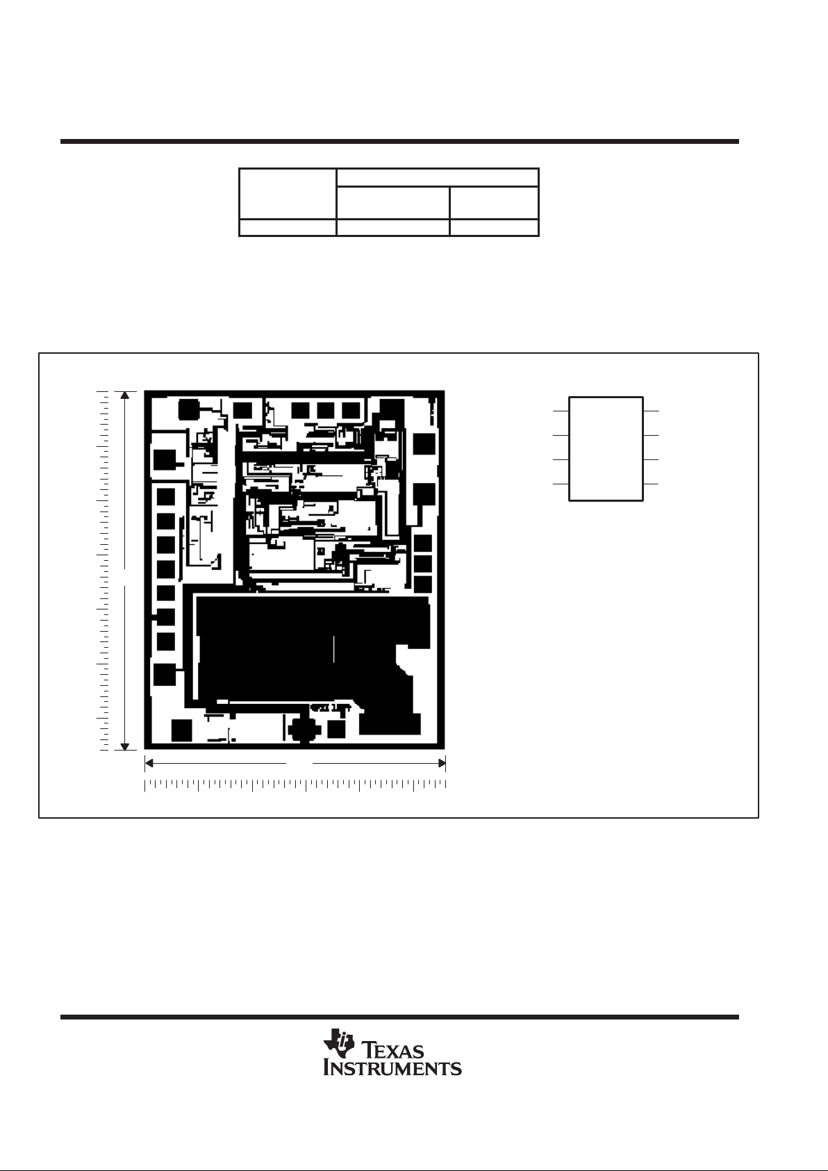
TPS6734 chip information
Thermal compression or ultrasonic bonding can be used on the doped-aluminum bonding pad. Chips can be
mounted with conductive epoxy or a gold-silicon preform. Contact factory for die sales.
CHIP THICKNESS: 15 TYPICAL
BONDING PADS: 4X4 MINIMUM
TJmax = 150°C
TOLERANCES ARE ±10%
ALL DIMENSIONS ARE IN MILS.
BONDING PAD ASSIGNMENTS
4
3
5
5
6
7
7
8
2
1
(1)
(2)
(3)
(4)
(5)
(5)
(6)
(7)
(7)
92
75
(8)
V
CC
FB
OUT
GND
EN
REF
SS
COMP
1
2
3
4
8
7
6
5
TPS6734
TPS6734I
FIXED 12-V 120-mA BOOST-CONVERTER SUPPLY
SLVS127A – AUGUST 1995 – REVISED JANUAR Y 1999
3
POST OFFICE BOX 655303 • DALLAS, TEXAS 75265
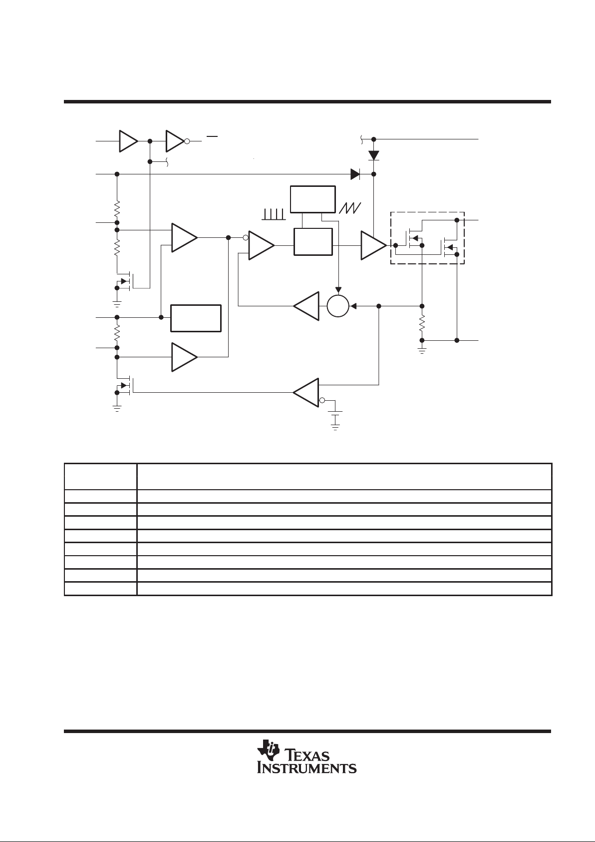
functional block diagram
EN
1
EN
7
EN
FB
_
+
4
COMP
Voltage
Reference
x3.5
SS
Clamp
Error
Amplifier
PWM
Comparator
R
S
170-kHz
Oscillator
V
CC
Power Switch
Drive Latch
Σ
2
REF
3
SS
x6
Current
Sense Amplifier
Overcurrent
Comparator
Driver
V
CC
OUT
GND
8
6
5
+
1 MΩ
–
Q
Terminal Functions
TERMINAL
NAME NO.
DESCRIPTION
EN 1 Enable. EN ≥2 V turns on the TPS6734. EN ≤ 0.4 V turns it off and reduces the supply current to 3 µA max.
REF 2 1.22-V reference voltage output. REF can source 100 µA for external loads.
SS 3 Soft Start. A capacitor between SS and GND brings the output voltage up slowly at power-up.
COMP 4 Compensation connection. A 0.001-µF capacitor between COMP and FB stabilizes the feedback loop.
GND 5 Ground
OUT 6 N-channel MOSFET drain connection
FB 7 Feedback voltage. FB is connected to the converter output for the feedback loop.
V
CC
8 Supply voltage input

TPS6734I
FIXED 12-V 120-mA BOOST-CONVERTER SUPPLY
SLVS127A – AUGUST 1995 – REVISED JANUAR Y 1999
4
POST OFFICE BOX 655303 • DALLAS, TEXAS 75265
detailed description
The following descriptions refer to the functional block diagram.
reference
The internal 1.22-V reference is brought out on REF and can source 100 µA maximum to external loads. A
0.01-µF to 0.1-µF decoupling capacitor connected between REF and GND is recommended to minimize noise
pickup.
oscillator and ramp generator
The oscillator circuit provides a 170-kHz clock, to set the converter operating frequency , and a timing ramp for
slope compensation. The clock waveform is a pulse, a few hundred nanoseconds in duration, that is used to
limit the maximum power-switch duty cycle to 95%. The timing ramp is summed with the current-sense signal
at the input to the current-sense amplifier.
driver latch
The latch, which consists of a set/reset flip-flop and associated logic, is used to control the state of the power
switch by turning the driver on and off. A high output from the latch turns the switch on; a low output from the
latch turns it off. In normal operation, the flip-flop is set high during the clock pulse, but gating keeps the latch
output low until the clock pulse is over. The latch is reset when the PWM comparator output goes high.
current-sense amplifier
The current-sense amplifier has a fixed gain of 6. It amplifies the slope-compensated current-sense voltage (a
summation of the voltage on the current-sense resistor and the oscillator ramp) and feeds it to the PWM
comparator.
error amplifier
The error amplifier is a high-gain differential amplifier used to regulate the converter output voltage. The
amplifier generates an error signal, which is fed to the PWM comparator. The error signal is generated when
a sample of the output voltage is compared to the internal reference and the difference is amplified. The output
sample is obtained from a resistive divider connected between FB and GND. FB is externally connected to the
converter output, and the divider output is connected to both the error amplifier input and COMP. A 0.001-µF
capacitor connected between FB and COMP stabilizes the voltage control loop.
PWM comparator
The PWM comparator resets the drive latch and turns off the power switch whenever the slope-compensated
current-sense signal from the current-sense amplifier exceeds the error signal.
power switch
The power switch is a 0.7-Ω n-channel MOSFET with current-sensing. The drain is connected to OUT and the
current sense is connected to a resistor. The voltage across the resistor is proportional to the current in the
power switch and is tied to the overcurrent comparator and the current-sense amplifier. In normal operation,
the power switch is turned on at the start of each clock cycle and turned off when the PWM comparator resets
the drive latch.
SS clamp
The SS (soft-start) clamp circuit limits the signal level on error-amplifier output during start-up. The voltage on
SS is amplified and used to momentarily override the error-amplifier output until it rises above that output, at
which point the error-amplifier takes over. This prevents the input to the PWM comparator from exceeding its
common-mode range (the error-amplifier output too high to be reached by the current ramp) by limiting the
maximum voltage on the error-amplifier output during start-up.
TPS6734I
FIXED 12-V 120-mA BOOST-CONVERTER SUPPLY
SLVS127A – AUGUST 1995 – REVISED JANUAR Y 1999
5
POST OFFICE BOX 655303 • DALLAS, TEXAS 75265
soft start
Soft start causes the output voltage to increase to the regulation point at a controlled rate of rise. The voltage
on the charging soft-start capacitor gradually raises the clamp on the error-amplifier output voltage, limiting
surge currents at power-up by increasing the current-limit threshold on a cycle-by-cycle basis. Even if SS has
no capacitor installed, some distributed capacitance will always be present. A soft-start cycle is initiated when
either the enable signal (EN) is switched high, or an overcurrent fault condition triggers the discharge of the
soft-start capacitor.
overcurrent comparator
The overcurrent comparator monitors the current in the power switch. The comparator trips and initiates a
soft-start cycle if the power-switch current exceeds 1.5-A peak. On each clock cycle, the power switch turns on
and attempts to deliver current until the overcurrent limits are exceeded.
enable (EN)
A logic low on EN puts the TPS6734 in shutdown mode. In shutdown, the output power switch, voltage
reference, and other functions are shut off, the supply current is reduced to 3 µA maximum, and the soft-start
capacitor is discharged through a 1-MΩ resistance. The output voltage falls to a diode drop below the input
voltage because of the current path from input to output through the inductor and diode.
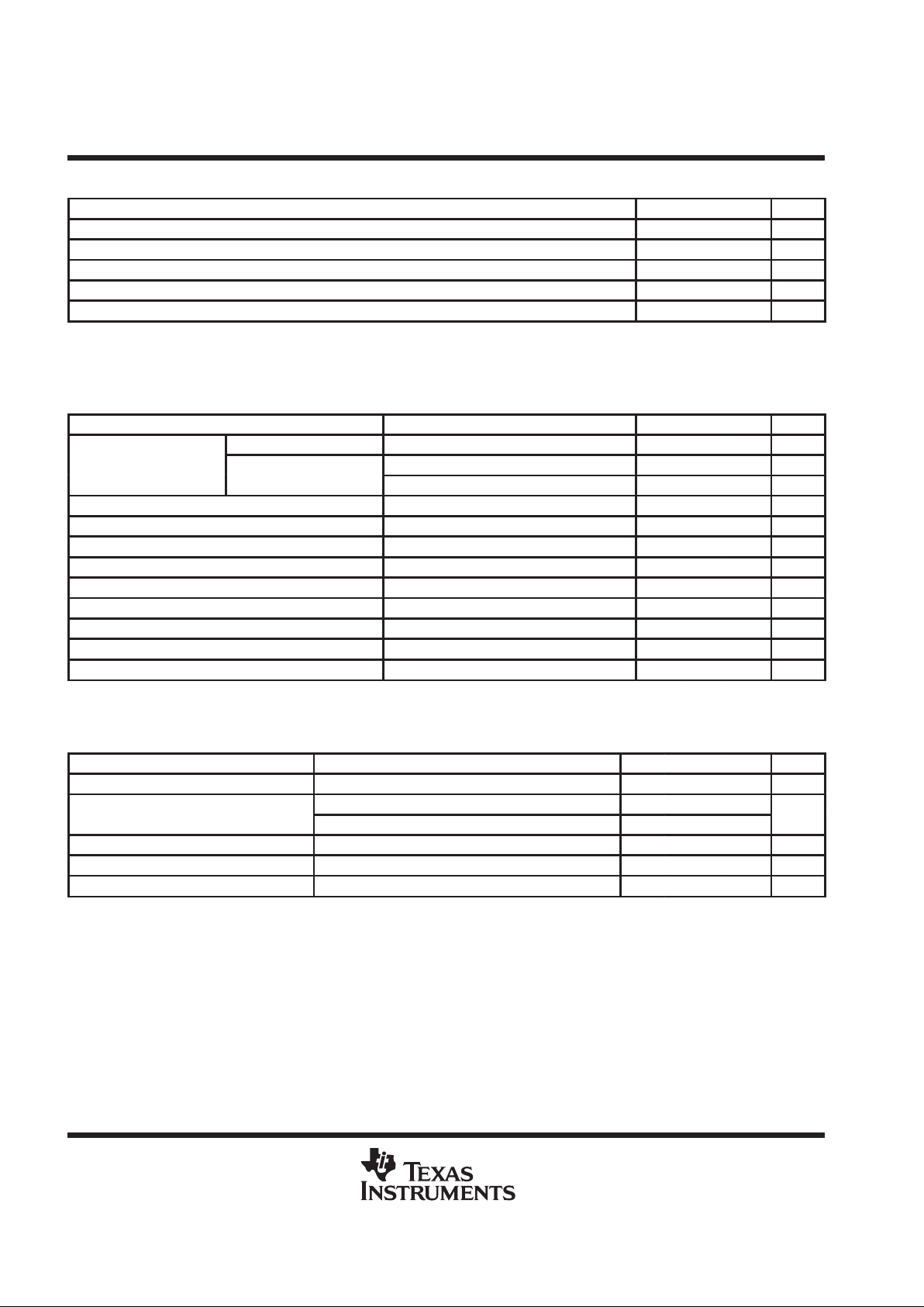
DISSIPATION RATING TABLE
PACKAGE
TA ≤ 25°C
POWER RATING
DERATING FACTOR
ABOVE TA = 25°C
TA = 70°C
POWER RATING
TA = 85°C
POWER RATING
D 725 mW 5.8 mW/°C 464 mW 377 mW
P 1175 mW 9.4 mW/°C 752 mW 611 mW
absolute maximum ratings over operating free-air temperature range (unless otherwise noted)
†
Pin voltages: V
CC,
OUT (see Note 1) –0.3 V to 15 V. . . . . . . . . . . . . . . . . . . . . . . . . . . . . . . . . . . . . . . . . . . . . . .
SS, COMP, EN (see Note 1) –0.3 V to V
CC
+ 0.3 V. . . . . . . . . . . . . . . . . . . . . . . . . . . . . . . . . . . .
Peak switch current 1.5 A. . . . . . . . . . . . . . . . . . . . . . . . . . . . . . . . . . . . . . . . . . . . . . . . . . . . . . . . . . . . . . . . . . . . . . .
Reference current 2.5 mA. . . . . . . . . . . . . . . . . . . . . . . . . . . . . . . . . . . . . . . . . . . . . . . . . . . . . . . . . . . . . . . . . . . . . . . .
Continuous power dissipation See Dissipation Rating Table. . . . . . . . . . . . . . . . . . . . . . . . . . . . . . . . . . . . . . . . .
Operating free-air temperature range, T
A
–40°C to 85°C. . . . . . . . . . . . . . . . . . . . . . . . . . . . . . . . . . . . . . . . . . . .
Storage temperature range, T
stg
–65°C to 150°C. . . . . . . . . . . . . . . . . . . . . . . . . . . . . . . . . . . . . . . . . . . . . . . . . . .
Lead temperature 1,6 mm (1/16 inch) from case for 10 s 260°C. . . . . . . . . . . . . . . . . . . . . . . . . . . . . . . . . . . . . .
†
Stresses beyond those listed under “absolute maximum ratings” may cause permanent damage to the device. These are stress ratings only, and
functional operation of the device at these or any other conditions beyond those indicated under “recommended operating conditions” is not
implied. Exposure to absolute-maximum-rated conditions for extended periods may affect device reliability.
NOTE 1: All voltage values are with respect to network terminal ground.
TPS6734I
FIXED 12-V 120-mA BOOST-CONVERTER SUPPLY
SLVS127A – AUGUST 1995 – REVISED JANUAR Y 1999
6
POST OFFICE BOX 655303 • DALLAS, TEXAS 75265
recommended operating conditions
MIN NOM MAX UNIT
Supply voltage 2.7 5 12 V
Compensation capacitor 0.001 µF
Output current at REF 0 100 µA
Reference capacitor 0.01 µF
Operating free-air temperature, T
A
–40 85 °C
electrical characteristics over recommended operating free-air temperature range, V
CC
= 5 V,
I
O(LOAD)
= 0 mA, EN = 5 V , typical values are at T
A
= 25°C (unless otherwise noted) (refer to circuit
shown in Figure 13)
PARAMETER TEST CONDITIONS MIN TYP MAX UNITS
Operating Entire circuit 1.2 2.5 mA
Supply current
EN = 0.4 V , entire circuit 3 µA
Standb
y
EN = 0.4 V, into V
CC
3 µA
High-level input threshold voltage at EN 2 V
Low-level input threshold voltage at EN 0.4 V
Shutdown input leakage current at EN –1 1 µA
On resistance at OUT Current at OUT = 500 mA 0.7 Ω
Leakage current at OUT VDS = 12 V 1 µA
Reference voltage 1.22 V
Reference drift TA = –40°C to 85°C 6.7 ppm/°C
Oscillator frequency 170 kHz
Compensation pin impedance 7500 Ω
performance characteristics over recommended operating free-air temperature range, typical
circuit connected as shown in Figure 13, typical values are at T
A
= 25°C (unless otherwise noted)
PARAMETER TEST CONDITIONS MIN TYP MAX UNITS
Output voltage VCC = 4.75 V , 0 mA < I
O(LOAD)
< 120 mA 11.64 12.12 12.6 V
VCC = 3.75 V 120 150
Load current
VCC = 3.0 V, Figure 11 150
mA
Line regulation VCC = 5 V to 12 V, I
O(LOAD)
= 50 mA 0.20%
Load regulation I
O(LOAD)
= 0 mA to 120 mA 0.0042%
Efficiency VCC = 5 V, I
O(LOAD)
= 120 mA 86%
 Loading...