

Page 1
User's Guide
SLVUB62A–June 2017–Revised June 2018
TPS65988 Evaluation Module
This document is the user guide for the TPS65988 Evaluation Module (TPS65988EVM). The
TPS65988EVM allows for evaluation of the TPS65988 IC as part of a stand-alone testing kit and for
development and testing of USB Type-C and Power Delivery (PD) end products. Out of the box, the
TPS65988EVM is configured to emulate a dual-port laptop computer. Both ports can be used to source or
sink power, and both are dual-role ports (DRP) but only support data as a downstream-facing port (DFP)
host. When different configurations are required to test your system, use the TPS65988 Application
Configuration software tool to create a configuration or load a different configuration template (see
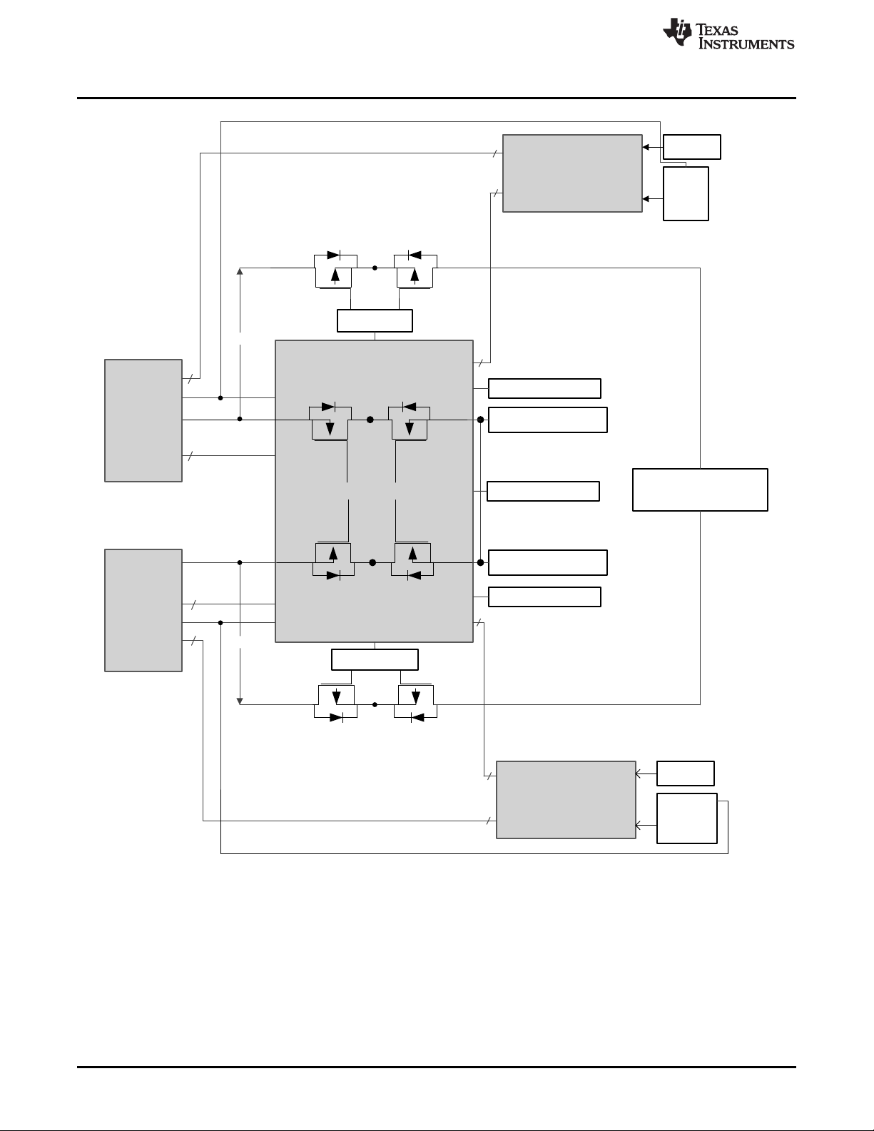
Figure 1). The TPS65988EVM uses a control MUX (HD3SS3412) to route DisplayPort™ (DP) and a USB
HUB (TUSB8020) to route USB signals to the appropriate port A or port A (port A/B). The control MUX
and USB HUB are connected to a SuperSpeed (SS) MUX (TUSB546) which routes the appropriate DP
lanes and USB 3.0 signals according to cable orientation and Alternate Mode selection. Figure 2 highlights
these features.
SLVUB62A–June 2017–Revised June 2018
Submit Documentation Feedback
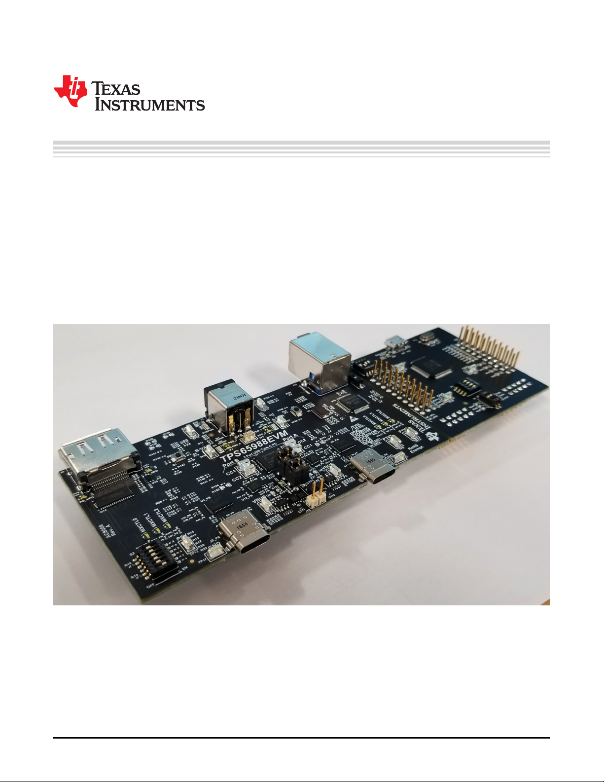
Figure 1. TPS65988EVM
Copyright © 2017–2018, Texas Instruments Incorporated
TPS65988 Evaluation Module
1
Page 2
TPS65988
PP1_CABLE
PP2_CABLE
VIN_3V3
System 3.3V
VBUS2
Type C
Receptacle
C1_CC1/2CC1/2
VBUS1
C2_CC1/2CC1/2
PPEXT2
PFET Control
PFET Control
PPEXT1
PPHV
1
PPHV2
I2C1
I2C2
USB2.0
System Power (20V) DC
Barrel Jack
C_SSTX/RX
5/9/15/20V @3A
Variable DC/DC
5/9/15/20V @3A
Variable DC/DC
Port A
Port B
I2C
DP0-3
AUX
C_SSTX
/RX
TUSB546
System 5V
System 5V
BC1.2
Sink
Sink
GPIO
MUX_CTR
L0-2
I2C
DP0-3
AUX
C_SSTX
/RX
TUSB546
DP
source
USB2
USB
source
USB3
MUX_CTR
L0-2
USB2.0
C_SSTX/RX
BC1.2
GPIO
DP
source
USB2
USB
source
USB3
Copyright © 2017, Texas Instruments Incorporated
www.ti.com
2
TPS65988 Evaluation Module
Figure 2. TPS65988EVM Block Diagram
Copyright © 2017–2018, Texas Instruments Incorporated
SLVUB62A–June 2017–Revised June 2018
Submit Documentation Feedback
Page 3

www.ti.com
1 About this Manual............................................................................................................ 6
2 Information About Cautions and Warnings............................................................................... 6
3 Items Required for Operation .............................................................................................. 6
4 Introduction ................................................................................................................... 6
5 Setup .......................................................................................................................... 7
6 Using the TPS65988EVM................................................................................................. 30
7 Connecting the EVM....................................................................................................... 30
8 TPS65988EVM Schematic................................................................................................ 40
9 TPS65988EVM Board Layout ............................................................................................ 53
10 TPS65988EVM Bill of Materials .......................................................................................... 57
1 TPS65988EVM............................................................................................................... 1
2 TPS65988EVM Block Diagram ........................................................................................... 2
3 TPS65988 Jumper Configuration.......................................................................................... 8
4 TPS65988 Jumper Configuration Net Names ........................................................................... 8
5 TPS65987D Jumper Configuration........................................................................................ 9
6 TPS65987D Jumper Configuration Net Names ......................................................................... 9
7 TPS65987S Jumper Configuration ...................................................................................... 10
8 TPS65987S Jumper Configuration Net Names ........................................................................ 10
9 DisplayPort™ Source Schematic Block ................................................................................. 11
10 DisplayPort™ Source Block Diagram ................................................................................... 11
11 DisplayPort™ Source Receptacle........................................................................................ 11
12 HRESET Push-Button (S1) Schematic.................................................................................. 12
13 HRESET Push-Button (S1) ............................................................................................... 12
14 SPI-MISO Pull Down Switch.............................................................................................. 13
15 FTDI
16 FTDI
17 I
18 I
19 Barrel Jack (J1) Schematic ............................................................................................... 16
20 Barrel Jack (J1)............................................................................................................. 16
21 Barrel Jack Detect Schematic ............................................................................................ 17
22 USB Type-B Receptacle (J11) Schematic.............................................................................. 17
23 USB (J11) Block Diagram................................................................................................. 17
24 USB Type-B Receptacle (J11) ........................................................................................... 18
25 USB Type-C™ Receptacles (J2) Schematic ........................................................................... 19
26 USB Type-C™ Receptacles (J2) ........................................................................................ 19
27 USB Micro-B Receptacle (J9) Schematic............................................................................... 20
28 USB Micro-B Receptacle (J9) ............................................................................................ 20
29 TP13 (5 V), TP8 (3.3 V), and TP12 (1.2 V)............................................................................. 21
30 Aardvark™ Connector (J10) Schematic................................................................................. 22
31 Aardvark™ Connector (J10) .............................................................................................. 22
Contents
5.1 Switch, Push Button, Connector, and Test Point Descriptions ............................................... 7
5.2 LED Indicators Description....................................................................................... 26
6.1 Powering the TPS65988EVM ................................................................................... 30
6.2 Firmware Configurations ......................................................................................... 30
7.1 Connecting to Various Devices ................................................................................. 30
7.2 Debugging the EVM............................................................................................... 38
List of Figures
®
Dip Switch (S3) Schematic ....................................................................................... 13
®
Dip Switch (S3)..................................................................................................... 14
2
C and BusPower DIP Switch (S2)...................................................................................... 15
2
C DIP Switch (S2) Schematic........................................................................................... 15
SLVUB62A–June 2017–Revised June 2018
Submit Documentation Feedback
Copyright © 2017–2018, Texas Instruments Incorporated
TPS65988 Evaluation Module
3
Page 4

www.ti.com
32 TP10, TP11, TP15, TP16, TP17, TP18, TP9: GND Test Points..................................................... 22
33 TP1, TP2, TP3 and TP4 – CC1 and CC2 Test Points ................................................................ 23
34 TPS65988 BMC Data...................................................................................................... 23
35 VBUS Test Points: TP14 ................................................................................................. 24
36 TPS65988 VBUS Voltage Transition .................................................................................... 24
37 A-Var, B-Var and System Power Test Points: TP7, TP6, and TP5.................................................. 25
38 BoosterPack™ Headers (J3 and J4) .................................................................................... 26
39 MUX Control LEDs......................................................................................................... 27
40 HPD Port A/B LEDs........................................................................................................ 27
41 PDO Port A/B LEDs........................................................................................................ 28
42 Connecting EVM to Type-A Device...................................................................................... 30
43 Connecting EVM to USB Type-C™ Device............................................................................. 31
44 Connecting EVM to USB Type-C™ Devices ........................................................................... 31
45 DP and USB Test Setup .................................................................................................. 37
46 DRP CC1 and CC2 Toggling ............................................................................................. 38
47 USB Type-C™ Connection and VBUS ................................................................................. 38
48 USB Type-C™ Connection and PD Negotiation ....................................................................... 39
49 TPS65988EVM Block Diagram........................................................................................... 40
50 TPS65988EVM Processor Block......................................................................................... 41
51 TPS65988EVM Power Path Block ...................................................................................... 42
52 TPS65988EVM Power Supply Block .................................................................................... 43
53 TPS65988EVM DisplayPort Mux......................................................................................... 44
54 TPS65988EVM SS MUX Block Port A .................................................................................. 45
55 TPS65988EVM SS MUX Block Port B .................................................................................. 46
56 TPS65988EVM USB HUB ................................................................................................ 47
57 TPS65988EVM USB Type-C™ Port-A Block........................................................................... 48
58 TPS65988EVM USB Type-C™ Port B Block........................................................................... 49
59 TPS65988EVM FTDI
®
Connector Block ................................................................................ 50
60 TPS65988EVM Current Sense Block Port A ........................................................................... 51
61 TPS65988EVM Current Sense Block Port B ........................................................................... 51
62 TPS65988EVM BoosterPack Header Block............................................................................ 52
63 TPS65988EVM Top Overlay.............................................................................................. 53
64 TPS65988EVM Top Layer Component View........................................................................... 53
65 TPS65988EVM SSTXRX1 ................................................................................................ 53
66 TPS65988EVM GND Plane 1 ............................................................................................ 54
67 TPS65988EVM High Speed .............................................................................................. 54
68 TPS65988EVM GND Plane 2 ............................................................................................ 54
69 TPS65988EVM Power 1 .................................................................................................. 55
70 TPS65988EVM Power 2 .................................................................................................. 55
71 TPS65988EVM GND Plane 3 ............................................................................................ 55
72 TPS65988EVM SSTXRX2 ................................................................................................ 56
73 TPS65988EVM Bottom Overlay.......................................................................................... 56
74 TPS65988EVM Bottom Layer Component View....................................................................... 56
List of Tables
1 Port A SS MUX Control LED Functions................................................................................. 27
2 Port B SS MUX Control LED Functions................................................................................. 28
3 Variable DC/DC Control Port A/B Functions............................................................................ 28
4 PDO LED 0 and PDO LED 1 Truth Table .............................................................................. 29
4
TPS65988 Evaluation Module
Copyright © 2017–2018, Texas Instruments Incorporated
SLVUB62A–June 2017–Revised June 2018
Submit Documentation Feedback
Page 5

www.ti.com
5 I
6 ADCIN1 Setting............................................................................................................. 29
7 DisplayPort™ and USB Test Setup...................................................................................... 33
8 TPS65988EVM Bill of Materials .......................................................................................... 57
Trademarks
BoosterPack is a trademark of Texas Instruments.
Dell is a registered trademark of Dell Incorporated.
FTDI, Future Technology Devices International are registered trademarks of Future Technology Devices
International Limited.
Microsoft, Windows are registered trademarks of Microsoft Corporation.
Aardvark is a trademark of Total Phase, Incorporated.
Total Phase is a registered trademark of Total Phase, Incorporated.
USB Type-C is a trademark of USB Implementers Forum.
DisplayPort is a trademark of Video Electronics Standards Association.
All other trademarks are the property of their respective owners.
2
C Address Setting ........................................................................................................ 29
SLVUB62A–June 2017–Revised June 2018
Submit Documentation Feedback
Copyright © 2017–2018, Texas Instruments Incorporated
TPS65988 Evaluation Module
5
Page 6

ATTENTION
STATIC SENSITIVE DEVICES
HANDLE ONLY AT
STATIC SAFE WORK STATIONS
About this Manual
1 About this Manual
This user's guide describes the TPS65988EVM. The guide consists of an introduction, setup instructions,
the EVM schematic, board layouts, component views, internal power (PWR) and ground (GND) plane
layouts, and a bill of materials (BOM).
2 Information About Cautions and Warnings
This EVM contains components that can potentially be damaged by
electrostatic discharge. Always transport and store the EVM in the supplied
ESD bag when not in use. Handle using an antistatic wristband. Operate on an
antistatic work surface. For more information on proper handling, see
Electrostatic Discharge (ESD).
www.ti.com
CAUTION
3 Items Required for Operation
The following items are required to use the TPS65988EVM:
• TPS65988 data sheet
• TPS65988EVM
• TPS65988 Application Customization Tool
• 20-V barrel jack adapter or DC power supply (model # 492-BBGP)
• Passive USB Type-C™ cables
• USB Type-A to USB Micro-B cable
• USB Type-A to USB Type-B cable
• Mini-DisplayPort to DisplayPort cables
• Notebook with USB 2.0, USB 3.0, and DP capabilities
4 Introduction
The TPS65988 is a stand-alone USB Type-C and Power Delivery (PD) controller providing cable plug and
orientation detection at the USB Type-C connector. Upon cable plug and orientation detection, the
TPS65988 communicates on the CC line using the USB PD protocol. When cable detection and USB PD
negotiation are complete, the TPS65988 enables the appropriate power path and configures external
multiplexers and alternate mode settings.
This user guide describes how the TPS65988EVM can be used to test DisplayPort alternate mode as well
as USB Data. This guide also contains testing procedures of DP alternate mode as well as various PD
power configurations. The EVM is customizable through the TPS65988 Configuration Tool. Additionally,
the EVM is equipped with a Future Technology Devices International®(FTDI®) board and Aardvark
connector to SPI or I2C interfaces for debugging and development.
6
TPS65988 Evaluation Module
Copyright © 2017–2018, Texas Instruments Incorporated
SLVUB62A–June 2017–Revised June 2018
Submit Documentation Feedback
Page 7

www.ti.com
5 Setup
This section describes the various EVM features and how to test these features. Schematic screen shots,
pictures, and block diagrams are provided as necessary.
5.1 Switch, Push Button, Connector, and Test Point Descriptions
Components described in this section are listed with respect to the EVM from left to right and top to
bottom. Related components are listed simultaneously.
5.1.1 Power Path Jumper Configuration
The TPS65988EVM allows for analysis of TPS65987D and TPS65987S platforms through the adjustment
of jumpers on J11 and J12.
Setup
SLVUB62A–June 2017–Revised June 2018
Submit Documentation Feedback
Copyright © 2017–2018, Texas Instruments Incorporated
TPS65988 Evaluation Module
7
Page 8

Setup
5.1.1.1 TPS65988 Jumper Configuration
Out of the box, the TPS65988EVM has jumper configuration for a TPS65988 device. With this
configuration, the two internal power paths are configured as Source paths for their respective Type-C
ports. The two external power paths are configured as Sink paths for their respective Type-C ports. When
using the TPS65988EVM, use a TPS65988 template in the TPS6598x Application Customization Tool.
Refer to Figure 3 and Figure 4 for the TPS65988 Jumper Configuration.
www.ti.com
Figure 3. TPS65988 Jumper Configuration
Figure 4. TPS65988 Jumper Configuration Net Names
8
TPS65988 Evaluation Module
Copyright © 2017–2018, Texas Instruments Incorporated
SLVUB62A–June 2017–Revised June 2018
Submit Documentation Feedback
Page 9
www.ti.com
5.1.1.2 TPS65987D Jumper Configuration
To use the TPS65988EVM to perform as a TPS65987D, the jumpers on J11 and J12 needs to be
adjusted. Place a jumper on J12 to short the two VBUS nodes together. In this use case, one of the
internal power paths is used as a source path and the other internal power path is used as a sink path.
The TPS65987D supports one Type-C port and contains 2 internal power paths. The TPS65988 can be
configured to act as a TPS65987D through the use of a TPS65987D Configuration Template in the
TPS6598x Application Customization Tool. In this configuration, PPHV2 is used as the Source path for the
Type-C port, it is connected to the net B-Var which is the Variable DC/DC used for Port B in the
TPS65988 configuration. PPHV1 is used for the Sink path on the TPS65987D. PPHV1 connects to the net
SYSPWR in this configuration. Refer to Figure 5 and Figure 6 for the TPS65987D Jumper Configuration.
When the TPS65988EVM is configured as a TPS65987D, only Port A is functional.
Setup
Figure 5. TPS65987D Jumper Configuration
Figure 6. TPS65987D Jumper Configuration Net Names
SLVUB62A–June 2017–Revised June 2018
Submit Documentation Feedback
Copyright © 2017–2018, Texas Instruments Incorporated
TPS65988 Evaluation Module
9
Page 10
Setup
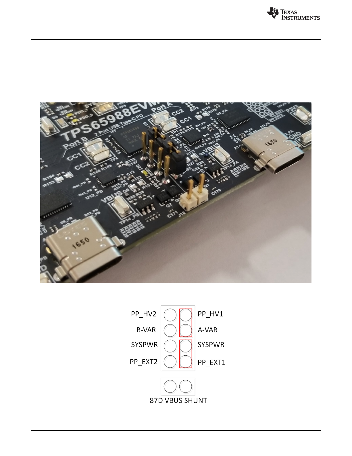
5.1.1.3 TPS65987S Jumper Configuration
To emulate a TPS65987S with the TPS65988EVM, the jumpers on J11 need to be adjusted. The
TPS65987S supports one Type-C port and contains one internal power path. When using the
TPS65988EVM to emulate a TPS65987S, the internal power path (PPHV1) is used as the Source Path
and one of the external power paths is used as the sink path. The TPS65988 can be configured to act as
a TPS65987S through the use of a TPS65987S Configuration Template in the TPS6598x Application
Customization Tool. Refer to Figure 7 and Figure 8 for the TPS65987D Jumper Configuration. When the
TPS65988EVM is configured as a TPS65987S, only Port A is functional.
www.ti.com
10
Figure 8. TPS65987S Jumper Configuration Net Names
TPS65988 Evaluation Module
Figure 7. TPS65987S Jumper Configuration
SLVUB62A–June 2017–Revised June 2018
Copyright © 2017–2018, Texas Instruments Incorporated
Submit Documentation Feedback
Page 11
HD3SS3412
TUSB546
DisplayPort
Source
Receptacle
LNA
LNB
LNC
LND
DP0
DP1
DP2
DP3
Port A
Port B
DP0
DP1
DP2
DP3
BDP0
BDP1
BDP2
BDP3
DP0
DP1
DP2
DP3
ADP0
ADP1
ADP2
ADP3
TUSB546
Copyright © 2017, Texas Instruments Incorporated
www.ti.com
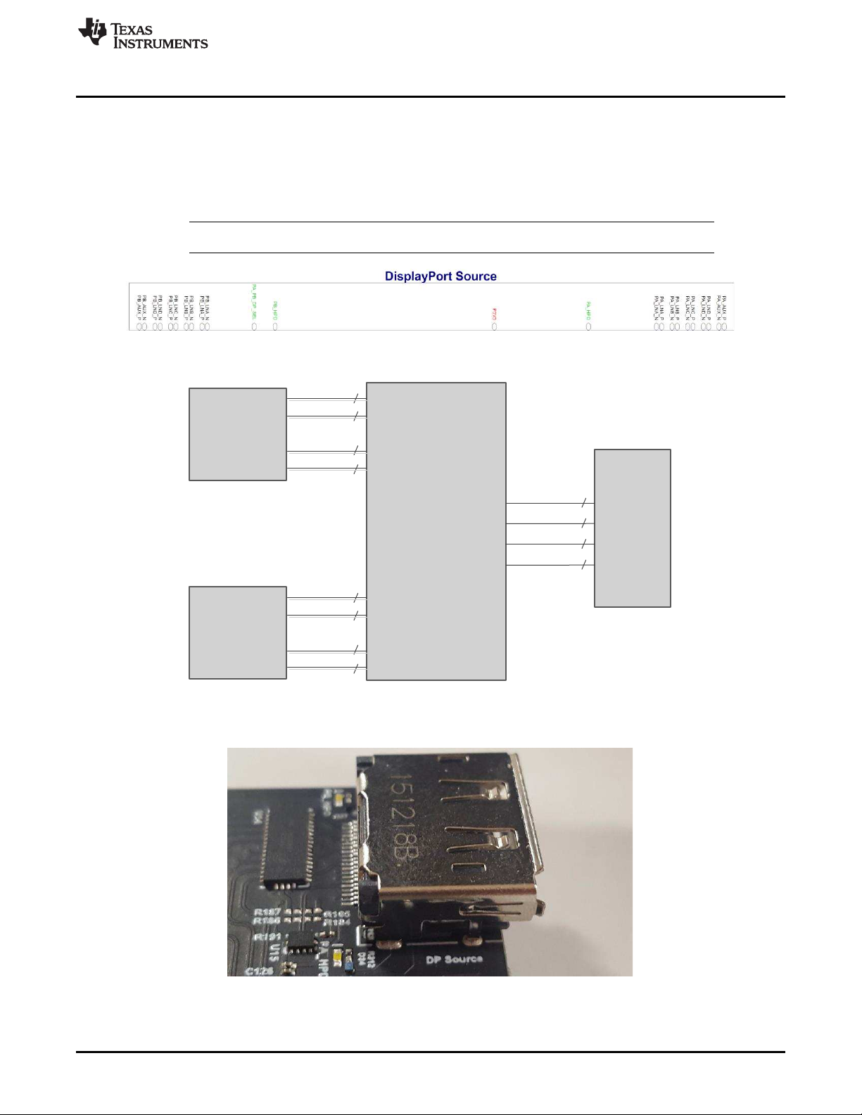
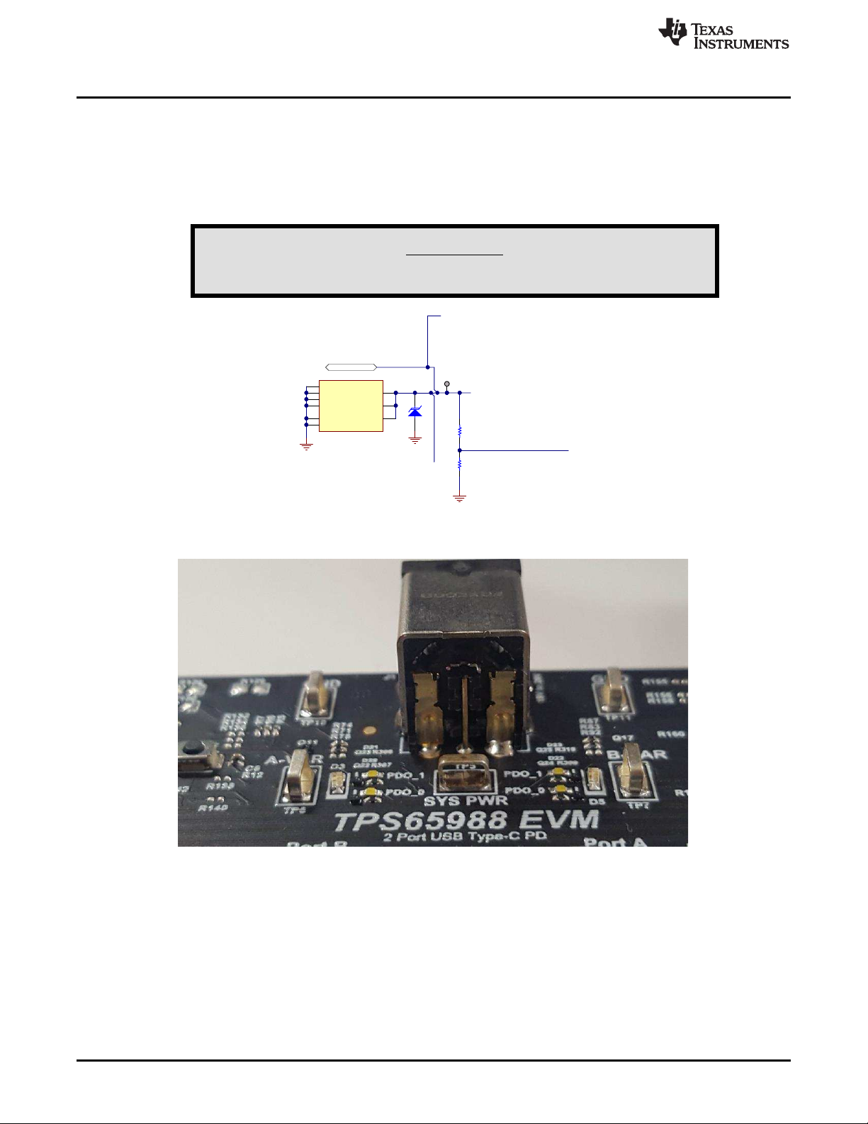
5.1.2 DP Source Receptacle
The DP source receptacle routes DP lanes for port A/B, AUX for port A/B, HPD for port A/B, as well as DP
port A/B select. The HD3SS3412 is used to MUX the DP source from the full-size DP receptacle to the
USB Type-C alternate mode MUX (TUSB546) for port A/B. Only one of the ports can support DP at a
time. The DP source MUX is controlled by GPIO0 that allocates the DP source signals to the appropriate
port. Figure 9 shows the DP source MUX Configuration
NOTE: Only one DP source can be used on either port A or port B at the same time.
Figure 9. DisplayPort™ Source Schematic Block
Setup
Figure 10. DisplayPort™ Source Block Diagram
Figure 11. DisplayPort™ Source Receptacle
SLVUB62A–June 2017–Revised June 2018
Submit Documentation Feedback
Copyright © 2017–2018, Texas Instruments Incorporated
TPS65988 Evaluation Module
11
Page 12
ADCIN1
6
ADCIN2
8
HRESET
39
100k
R12
0.01µF
C6
GND
S1
P3V3
HRESET
0 R11
Setup
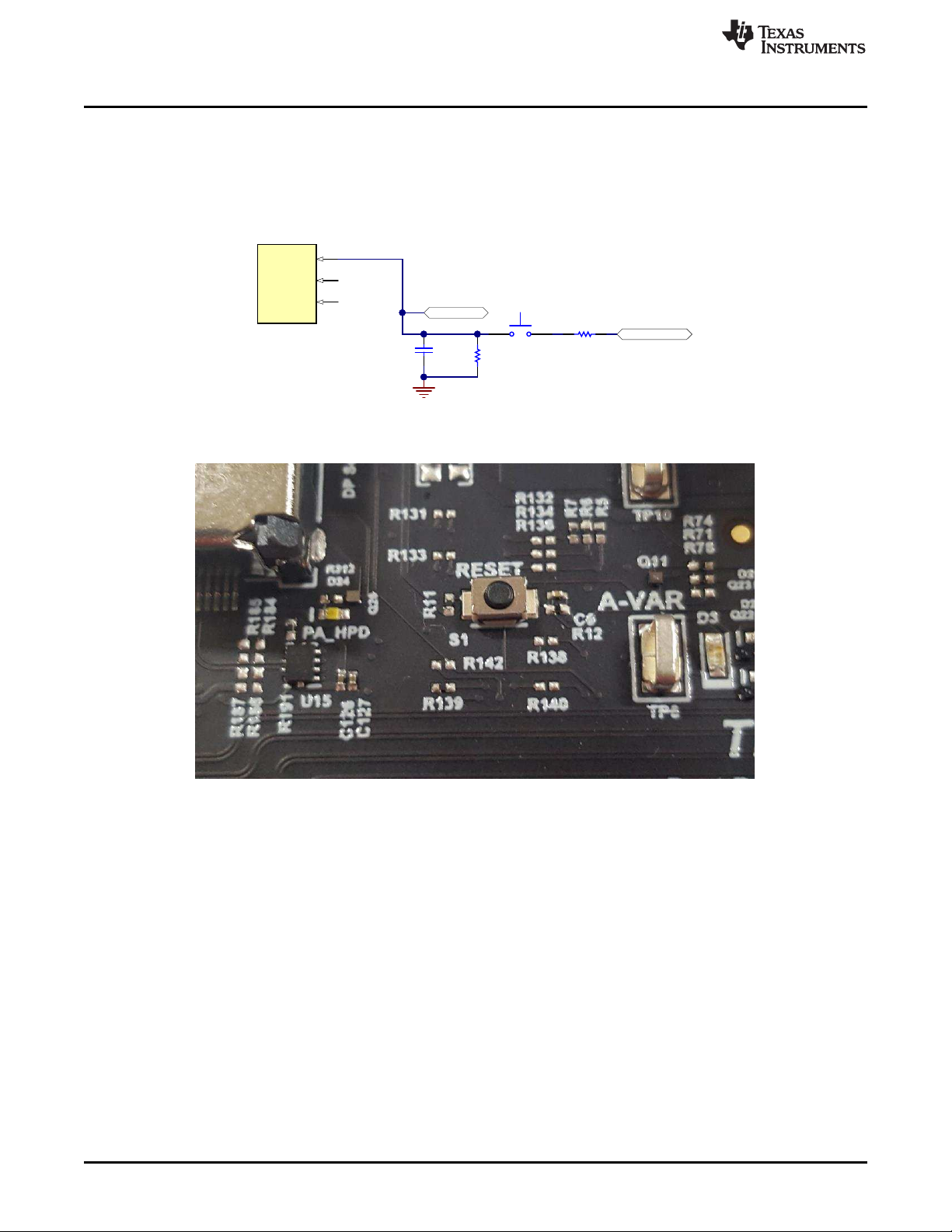
5.1.3 S1 HRESET Push-Button
S1 is located on the top-left corner of the EVM. This switch is a push-button that pulls the HRESET pin
(39) of the TPS65988 high when pressed. Releasing the push-button pulls HRESET low again, and the
TPS65988 goes through a soft reset, which consists of reloading firmware (FW) from RAM. If a valid
configuration is present in the RAM, the TPS65988 does not reload the configuration from the external
flash. Figure 12 highlights these features.
Figure 12. HRESET Push-Button (S1) Schematic
www.ti.com
Figure 13. HRESET Push-Button (S1)
12
TPS65988 Evaluation Module
SLVUB62A–June 2017–Revised June 2018
Copyright © 2017–2018, Texas Instruments Incorporated
Submit Documentation Feedback
Page 13
GND
0R203
DNP
0R206
DNP
0R212
0R215
0R218
0R222
0R204
DNP
0R207
DNP
0R209
DNP
0R219
0R223
1.00k
R195
F_SPI_CLK
F_I2C_IRQ2
F_I2C_SCL2
F_I2C_SDA2
F_SYSTEM_3V3
F_SYSTEM_3V3
F_5V_VBUS
F_SWD_CLK
F_SWD_DATA
F_C_UART_RX
F_C_UART_TX
1
3
5 6
4
2
7
9 10
8
1211
1413
1615
1817
2019
J6
63
1 8
2 7
54
S3
F_RESETN RESETN
F_I2C_IRQ1
White
1 2
D26
10.0k
R314
GND
3
1
2
Q28
I2C1_SCL
I2C1_SDA
www.ti.com
5.1.4 S6 SPI MISO Pull Down Button
S6 is located on the top right corner of the EVM. This push button switch holds the SPI Miso line to GND.
This button is to be used when booting the device. If this button is pressed when the device is booting, the
TPS65988 does not load its configuration from the SPI Flash, but instead boots into a default ROM
configuration.
Setup
5.1.5 S3: FTDI®Enable and Disable
The dip switch, S3, has 4 switches. The switches labeled 3.3V (switch 3) and 5V (switch 4) pass the
supply from the FTDI board micro-B receptacle from the BoosterPack header (J6) and vice versa. The
Force Enable (switch 1 and switch 2) switch controls the reset on the FTDI device. When switch 1 is
closed, the FTDI is held in reset until the TPS65988 has successfully loaded the firmware. When switch 2
is closed, the FTDI can be reset externally by pin 8 on the FTDI board header J7. By default, all switches
are opened and in the upward position. Figure 15 highlights these features.
SLVUB62A–June 2017–Revised June 2018
Submit Documentation Feedback
Figure 14. SPI-MISO Pull Down Switch
Figure 15. FTDI®Dip Switch (S3) Schematic
Copyright © 2017–2018, Texas Instruments Incorporated
TPS65988 Evaluation Module
13
Page 14

Setup
www.ti.com
Figure 16. FTDI®Dip Switch (S3)
5.1.6 S2: SPI , I2C, and BusPowerZ Configurations
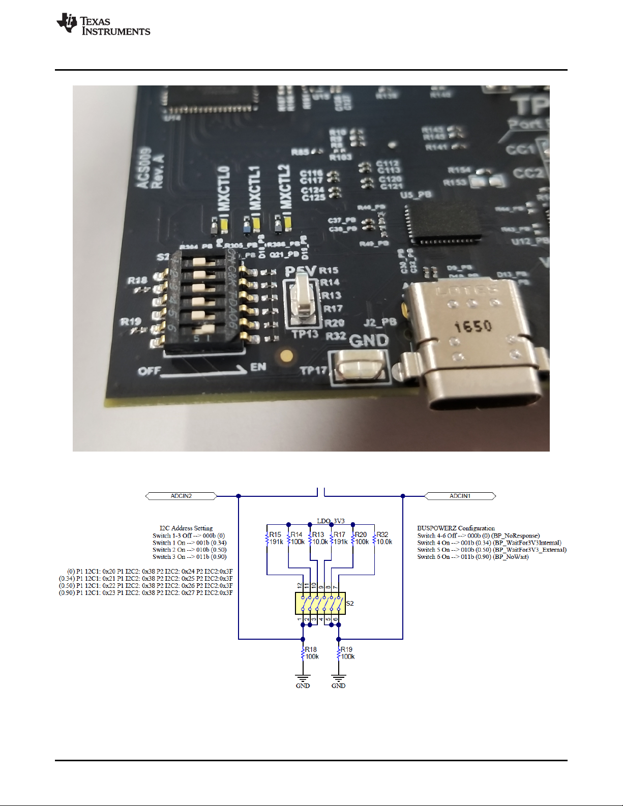
The TPS65988EVM has a dip switch (S2) that can be used to configure the I2C addresses and BusPower
settings of the device. Switch1 through Switch3 are used to set the I2C address of the TPS65988 by
adjusting the voltage divider seen at ADCIN2. Refer to the TPS65988 datasheet to see the different I2C
address configurations. The default switch setting for Switch 1 through switch 3 is open, resulting in a
0x38 I2C address. Switch4 through Switch6 adjusts the BusPowerZ setting by adjusting the voltage divider
on ADCIN1. Refer to the TPS65988 datasheet to see the different BusPowerZ configurations. Figure 17
highlights the default switch setting of S2.
14
TPS65988 Evaluation Module
Copyright © 2017–2018, Texas Instruments Incorporated
SLVUB62A–June 2017–Revised June 2018
Submit Documentation Feedback
Page 15
www.ti.com
Setup
Figure 17. I2C and BusPower DIP Switch (S2)
Figure 18. I2C DIP Switch (S2) Schematic
SLVUB62A–June 2017–Revised June 2018
Submit Documentation Feedback
Copyright © 2017–2018, Texas Instruments Incorporated
TPS65988 Evaluation Module
15
Page 16
SYS_PWR
100k
R71
D2
GND
SENSE
1
GND
4
POWER
2
POWER
3
GND
5
SHIELD
6
SHIELD
7
SHIELD
8
SHIELD
9
J1
JPD1135-509-7F
GND
SYS_PWR
TP5
11.0k
R74
GND
Setup
5.1.7 J1: Barrel Jack Power Connector
The barrel jack power connector accepts a 19-V to 20-V DC supply. A standard Dell or HP notebook
adapter (or similar adapter) provides the required power. This input provides the PP_HV power rail 19-V to
20-V for high power PD contracts up to 60 W per port or 120 W, total. An appropriate power adapter
greater than 120 W must be used for high-power PD. For example, the Dell®130-W Part Number: 492BBGP. Figure 19 highlights these features.
The barrel jack input is high voltage.
www.ti.com
WARNING
Figure 19. Barrel Jack (J1) Schematic
Figure 20. Barrel Jack (J1)
16
TPS65988 Evaluation Module
Copyright © 2017–2018, Texas Instruments Incorporated
SLVUB62A–June 2017–Revised June 2018
Submit Documentation Feedback
Page 17
TUSB546
TUSB546
DisplayPort
Source
Receptacle
LNA
LNB
LNC
LND
DP0
DP1
DP2
DP3
Port A
Port B
DP0
DP1
DP2
DP3
BDP0
BDP1
BDP2
BDP3
DP0
DP1
DP2
DP3
ADP0
ADP1
ADP2
ADP3
TUSB546
Copyright © 2017, Texas Instruments Incorporated
3
4
1
6
2
V+
V-
5
U10
TLV3012AIDCKR
560k
R115
DNP
39k
R112
DNP
GND
GND
Hysterisis
Vh 1.376V
Vl 1.16V
100k
R107
15.0k
R111
GND
Good @ 11.2V
!Good @9.5V
22pF
C85
GND
0
R108
0.1µF
C80
BJ_DETECT
0 R109
DNP
www.ti.com
5.1.8 Barrel Jack Detect
The TPS65988EVM is capable of requesting a power role swap when the barrel jack is connected on an
EVM that is currently bus-powered. The barrel jack voltage is sensed by a comparator, which drives
GPIO1 (BJ_DETECT) on the TPS65988. By default, the Barrel Jack Detect is not enabled. To enable
Barrel Jack Detect place R109 and refer to the TPS65988 Utilities Tool User Guide and TPS65988
Firmware User Guide. Figure 21 highlights these features.
Figure 21. Barrel Jack Detect Schematic
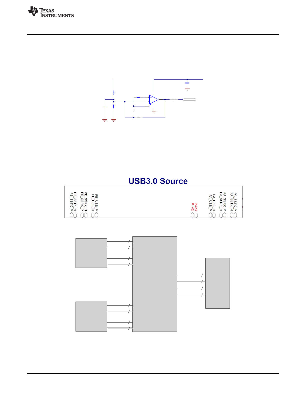
5.1.9 USB Type B Connector (J11)
J11 is the Type-B connection to the PC for testing USB 2.0 or USB 3.0 functionality. A Type-A to Type-B
cable can be used to connect the EVM to the USB port on a computer. This connector provides the USB
data to the USB HUB on the TPS65988EVM. Figure 22 through Figure 24 highlight these features.
Setup
SLVUB62A–June 2017–Revised June 2018
Submit Documentation Feedback
Figure 22. USB Type-B Receptacle (J11) Schematic
Figure 23. USB (J11) Block Diagram
Copyright © 2017–2018, Texas Instruments Incorporated
TPS65988 Evaluation Module
17
Page 18
Setup
www.ti.com
Figure 24. USB Type-B Receptacle (J11)
18
TPS65988 Evaluation Module
Copyright © 2017–2018, Texas Instruments Incorporated
SLVUB62A–June 2017–Revised June 2018
Submit Documentation Feedback
Page 19
www.ti.com
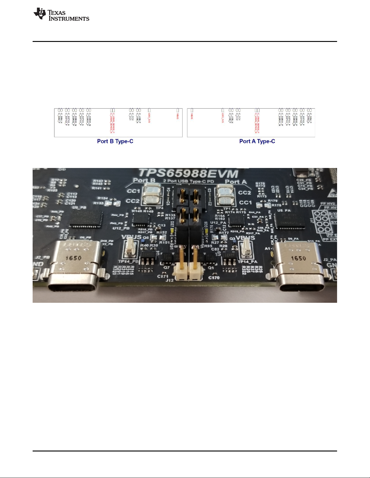
5.1.10 USB Type-C™Connector (J2)
The TPS65988EVM has two full feature USB Type-C receptacles (port A/B) and routes VBUS, SSTX and
SSRX pairs, SBU1 and SBU2 pairs, and D+ and D– signals. The TPS65988 device can be used in selfpowered and bus-powered configurations for added flexibility. When self-powered, the EVM can provide
up to 60 W (20 V, at 3 A) of power per port via the internal high voltage power path. The EVM is also
capable of sinking 100 W (20 V, at 5 A) of power via the external power path. The internal power path is
used for sourcing power and the external power path is used for sinking power. Figure 25 and Figure 26
highlight these features.
Figure 25. USB Type-C™ Receptacles (J2) Schematic
Setup
SLVUB62A–June 2017–Revised June 2018
Submit Documentation Feedback
Figure 26. USB Type-C™ Receptacles (J2)
Copyright © 2017–2018, Texas Instruments Incorporated
TPS65988 Evaluation Module
19
Page 20

GND
GND
26 ohmL7
0.01µF
C143
F_5V_VBUS
F_USB_D_P
F_USB_D_N
D16 D17
GND GND
VBUS
1
D-
2
D+
3
ID
4
GND
5
678
11109
J9
Setup
5.1.11 USB Micro B Connector (J9)
J9, the micro-B receptacle connects the FTDI to the PC for the TPS65988 Customization GUI. Use a
standard USB micro-B to Type-A cable to make this connection. The Debug Board Enable LED turns on
when VBUS is present on the FTDI board. Figure 27 and Figure 28 highlight these features.
Figure 27. USB Micro-B Receptacle (J9) Schematic
www.ti.com
Figure 28. USB Micro-B Receptacle (J9)
20
TPS65988 Evaluation Module
Copyright © 2017–2018, Texas Instruments Incorporated
SLVUB62A–June 2017–Revised June 2018
Submit Documentation Feedback
Page 21
www.ti.com
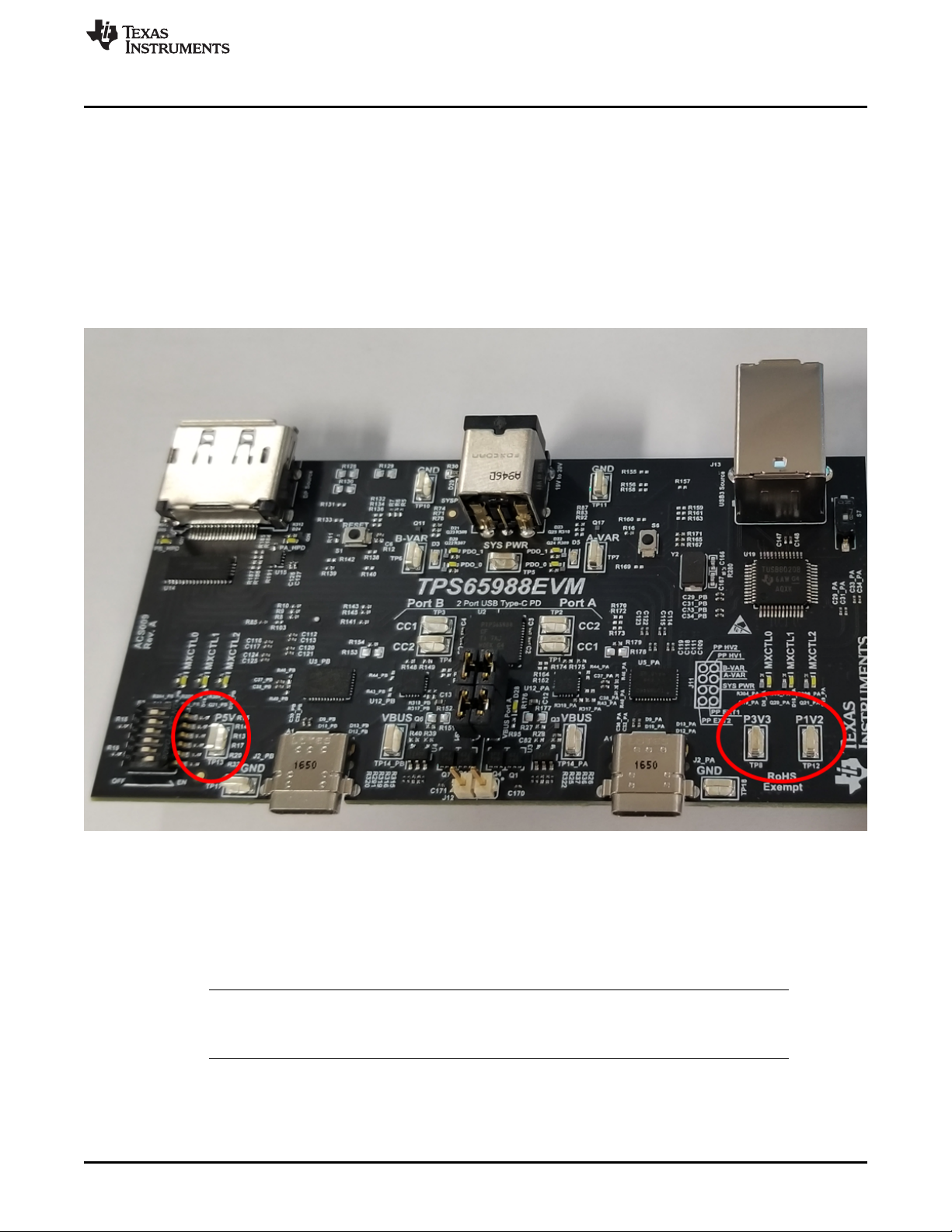
5.1.12 TP13 (5 V), TP8 (3.3 V), and TP12 (1.2 V)
Use the TP13, TP8, and TP12 test points to measure the output voltage of the onboard DC/DC
converters. These DC/DC converters produce the required voltage rails for full functionality of the EVM
including power delivery, powering internal and external circuits, and so forth. These test points allow the
user to verify the system supplies on the TPS65988EVM. LDO_1V8 is internally generated for internal
circuitry. Use P3V3 to supply VIN_3V3 which then supplies LDO_3V3. Also, use LDO_3V3 as a lowpower output for external flash memory. In bus-powered conditions, or self-powered conditions, P3V3 and
LDO_3V3 are active. P3V3 has the ability to operate at 4 V to compensate for IR drop through the USB
Type-C cable. The P5V supply can operate at 4.5 V at 100% duty cycle, but it is intended to supply the 5
V at 3 A when the barrel jack or system power is connected to the EVM. P5V powers PP_CABLE for both
ports as well as the VBUS current sense IC for both ports. Figure 29 highlights these test points.
Setup
Figure 29. TP13 (5 V), TP8 (3.3 V), and TP12 (1.2 V)
5.1.13 Aardvark™ Connector (J10)
This connector matches the Total Phase®Aardvark that allows the user to access the I2C and SPI pins on
the TPS65988EVM using the SPI, I2C master, or both capabilities. Figure 30 and Figure 31 highlight
theses features.
NOTE: The FT4232 loads the I2C or SPI pins when powered. TI recommends leaving the FT4232 in
reset by having the Force Enable switches (switch 1 and switch 2) in the disabled (up)
position.
SLVUB62A–June 2017–Revised June 2018
Submit Documentation Feedback
Copyright © 2017–2018, Texas Instruments Incorporated
TPS65988 Evaluation Module
21
Page 22

1 2
3 4
5 6
7 8
9 10
J10
0R256
0R257
0R258
0R259
0R261
0R260
0R254
DNP
0R255
DNP
Aardvark Connector
0
R262
GND
F_I2C_SCL2
F_I2C_SDA2
F_SPI_CLK F_SPI_MOSI
F_SPI_MISO
F_SPI_CSZ
I2C1_SCL
I2C1_SDA
Setup
www.ti.com
Figure 30. Aardvark™ Connector (J10) Schematic
Figure 31. Aardvark™ Connector (J10)
5.1.14 TP10, TP11, TP15, TP16, TP17, TP18, TP9: GND Test Points
TP15, TP16, and TP9 GND Test Points are provided for attaching an oscilloscope or multi-meter. Test
Points TP10, TP11, TP17, and TP18 (circled in orange) are used for load testing. These Test Points are
connected to the board GND planes through multiple vias.Figure 32 highlights these features.
22
Figure 32. TP10, TP11, TP15, TP16, TP17, TP18, TP9: GND Test Points
TPS65988 Evaluation Module
Copyright © 2017–2018, Texas Instruments Incorporated
SLVUB62A–June 2017–Revised June 2018
Submit Documentation Feedback
Page 23

www.ti.com
5.1.15 TP1, TP2, TP3 and TP4 – CC1 and CC2 Test Points
Test points CC1 and CC2 are used to tie a PD protocol analyzer for PD BMC data or to verify the BMC
signal integrity with an oscilloscope (depending on the cable orientation). Use a multimeter or oscilloscope
to measure VCONN when an electronically marked USB Type-C cable is connected. Use these test points
to attach an external load on VCONN. Figure 33 and Figure 34 the highlight these features.
Setup
Figure 33. TP1, TP2, TP3 and TP4 – CC1 and CC2 Test Points
Figure 34. TPS65988 BMC Data
SLVUB62A–June 2017–Revised June 2018
Submit Documentation Feedback
Copyright © 2017–2018, Texas Instruments Incorporated
TPS65988 Evaluation Module
23
Page 24

Setup
5.1.16 TP14 (PA and PB): VBUS Test Point
The VBUS test points are used to measure VBUS at each USB Type-C port A/B connector. With PD
power possibly going up to 20 V, use caution when connecting and disconnecting probes on the
TPS65988EVM. The VBUS test point is capable of drawing up to 3 A for an external load. Note that a PD
power contract with the necessary capability must be negotiated in order to draw current from the VBUS
test point. Refer to the TPS65988 Configuration Tool User Guide for configuration instructions. Figure 35
and Figure 36 highlights these features.
www.ti.com
Figure 35. VBUS Test Points: TP14
Figure 36. TPS65988 VBUS Voltage Transition
24
TPS65988 Evaluation Module
Copyright © 2017–2018, Texas Instruments Incorporated
SLVUB62A–June 2017–Revised June 2018
Submit Documentation Feedback
Page 25

www.ti.com
5.1.17 TP7, TP6, and TP5: A-VAR, B-VAR, and System Power Test Points Respectively
Test point A-VAR (TP7) is the output of the variable DC/DC for port A. Test point B-VAR (TP6) is the
output of the variable DC/DC for port B. These test points are provided for attaching an oscilloscope,
multimeter, or external supply. System power (TP5) can be in the operating range of 5–20 V, any voltage
lower than 20 V decreases the sourcing power capabilities. Figure 37 highlights these features.
Setup
Figure 37. A-Var, B-Var and System Power Test Points: TP7, TP6, and TP5
SLVUB62A–June 2017–Revised June 2018
Submit Documentation Feedback
Copyright © 2017–2018, Texas Instruments Incorporated
TPS65988 Evaluation Module
25
Page 26

0 R165
0 R169
DNP
0 R167
0 R159
DNP
0 R140
DNP
0 R160
DNP
0 R158
DNP
0 R155
DNP
0 R173
DNP
0 R172
DNP
0 R171
0 R146
DNP
0 R144
DNP
3.83k
R147
DNP
100k R150
DNP
GND
0 R139
0 R141
0 R143
0 R145
SWD_DATA
SWD_CLK
I2C1_IRQZ
SPI_MOSI
SPI_MISO
SPI_CLK
SPI_CS
LDO_3V3
P3V3 P5V
0 R156
DNP
I2C1_SDA
I2C1_SCL
GND
GND
I2C2_SCL
0 R131
DNP
0 R133
DNP
0 R135
DNP
0 R137
DNP
0 R162
DNP
0 R164
DNP
0 R166
DNP
0 R168
DNP
0 R132
DNP
0 R134
DNP
I2C2_IRQZ
I2C2_SDA
0 R136
DNP
0 R138
DNP
0 R142
DNP
ADCIN2
ADCIN1
GPIO0
0 R170
DNP
0 R174
0 R175
100k
R177
GND
100k
R152
GND
HRESET
LDO_3V3
LDO_1V8
0 R157
DNP
P1V2
PB_ISENSE_VOUT
PA_ISENSE_VOUT
100k
R179
GND
100k
R154
GND
1
3
5 6
4
2
7
9 10
8
1211
1413
1615
1817
2019
2221
2423
J3
SSW-112-22-G-D-VS
1
3
5 6
4
2
7
9 10
8
1211
1413
1615
1817
2019
2221
2423
J4
SSW-112-22-G-D-VS
PB_VBUS
PB_VAR_DCDC
PA_VBUS
PA_VAR_DCDC
PB_PP_EXT_ENABLE
PA_PP_EXT_ENABLE
PB_USB_P
PB_USB_N
PA_USB_P
PA_USB_N
PA_CC2
PA_CC1
100k
R176
DNP
100k
R178
DNP
100k
R151
DNP
100k
R153
DNP
0 R148
PB_CC1
0 R149
PB_CC2
0 R128
DNP
0 R129
DNP
0 R130
DNP
GPIO1
GPIO4
GPIO14
GPIO15
GPIO7
GPIO6
GPIO2
GPIO3
GPIO5
0 R163
DNP
0 R161
DNP
Copyright © 2017, Texas Instruments Incorporated
Setup
5.1.18 J3 and J4 (Bottom of EVM): Signal Headers
These headers allow the user to probe many different signals on the TPS65988EVM. Note that some of
the header pins are not connected unless a 0-Ω option resistor is placed. Figure 38 highlights these
features.
www.ti.com
5.2 LED Indicators Description
The EVM has multiple LEDs to notify the user what type of connection is present. The LEDs are
separated into two groups: MUX control LEDs (MXCTL0–2) and status LEDs. All LEDs are enabled with
Figure 38. BoosterPack™ Headers (J3 and J4)
general purpose I/O (GPIO); therefore, each must be enabled separately via configuration, if configuring a
26
custom image (see TPS65988 Configuration Tool User Guide). By default MXCTL0 LED is on when the
connected device supports USB3.0, MXCTL1 LED is on when DisplayPort Alternate Mode is entered.
MXCTL2 highlights the orientation of the cable. When MXCTL2 LED is on, CC2 is connected. When
MXCTL2 LED is off, CC1 is connected.
TPS65988 Evaluation Module
Copyright © 2017–2018, Texas Instruments Incorporated
SLVUB62A–June 2017–Revised June 2018
Submit Documentation Feedback
Page 27

www.ti.com
5.2.1 MXCTL0-2 and HPD LEDs (SS MUX Control LED)
These LEDs correspond to the MUX control signals needed for the SS MUX on either USB Type-C port.
Figure 39 and Figure 40 Table 1 highlight these features and Table 1 and Table 2 summarize the LED
behavior.
Figure 39. MUX Control LEDs
Setup
Table 1. Port A SS MUX Control LED Functions
LED Indicator GPIO Function
D6 - MXCTL0 GPIO6 USB 3.0 event
D18 - MXCTL1 GPIO5 DP mode event
D19 - MXCTL2 GPIO7 Cable orientation event
D24 - PA_HPD GPIO3 HPD
SLVUB62A–June 2017–Revised June 2018
Submit Documentation Feedback
Figure 40. HPD Port A/B LEDs
Copyright © 2017–2018, Texas Instruments Incorporated
TPS65988 Evaluation Module
27
Page 28

Setup
LED Indicator GPIO Function
D6 - MXCTL0 GPIO_1 USB 3.0 event
D18 - MXCTL1 GPIO_0 DP mode event
D19 - MXCTL2 GPIO_2 Cable orientation event
D25 - PB_HPD GPIO_4 HPD
5.2.2 Status LEDs
LEDs, D5 and D3, are for the variable DC/DC on port A, and port B, respectively. When powering up the
EVM, these LEDs lights up blue. They also provide a voltage discharge path for high to low PD contracts.
For higher voltage PD contracts, D5 and D3 are brighter. Figure 41 highlights these features and Table 3
summarizes the LED behavior.
www.ti.com
Table 2. Port B SS MUX Control LED Functions
28
LED Indicator GPIO Function
D20 - PA_PDO0 GPIO_12 PDO TT bit 0
D21 - PA_PDO1 GPIO_13 PDO TT bit 1
D23 - PB_PDO1 GPIO_14 PDO TT bit 1
D22 - PB_PDO0 GPIO_15 PDO TT bit 0
D5 - PA_VAR_DCDC GPIO_16 VAR-A enable
D3 - PB_VAR_DCDC GPIO_17 VAR-B enable
TPS65988 Evaluation Module
Figure 41. PDO Port A/B LEDs
Table 3. Variable DC/DC Control Port A/B Functions
SLVUB62A–June 2017–Revised June 2018
Copyright © 2017–2018, Texas Instruments Incorporated
Submit Documentation Feedback
Page 29

www.ti.com
The PDO LEDs in Table 4 are high, depending on which PDO is negotiated. By activating these LEDs, the
output voltage of the variable DC/DC can be changed. Table 4 summarizes the PDO LED behavior.
Table 4. PDO LED 0 and PDO LED 1 Truth Table
PDO PDO LED 1 PDO LED 0 R1 R2 Output Voltage
PDO 1 (5 V) 0 0 60.4 kΩ 19.1 kΩ 5.15 V
PDO 2 (9 V) 0 1 60.4 kΩ 9.27 kΩ 9.26 V
PDO 3 (15 V) 1 0 60.4 kΩ 5.2 kΩ 15.62 V
PDO 4 (20 V) 1 1 60.4 kΩ 4.04 kΩ 19.78 V
5.2.3 S2 Switch Bank Functionality
The I2C address setting must match the configuration generated by the TPS65988 configuration tool.
Table 5 summarizes the I2C address settings. To adjust the dead battery boot behavior, the setting on
ADCIN1 can be adjusted. Table 6 summarizes the ADCIN1 settings. The specific settings for each divider
ratio is discussed in the TPS65988 datasheet.
Switch On, Off Bits Divider Ratio
1-3 Off 000b 0.00
1 On 001b 0.34
2 On 010b 0.50
3 On 011b 0.90
Setup
Table 5. I2C Address Setting
Table 6. ADCIN1 Setting
Switch On, Off Bits Divider Ratio
4-6 Off 000b 0.00
4 On 001b 0.34
5 On 010b 0.50
6 On 011b 0.90
SLVUB62A–June 2017–Revised June 2018
Submit Documentation Feedback
Copyright © 2017–2018, Texas Instruments Incorporated
TPS65988 Evaluation Module
29
Page 30

Notebook
(DP & USB Source )
TPS65988-EVM
Flash DriveUSB Out
DP
source
USB
source
Using the TPS65988EVM
6 Using the TPS65988EVM
This section discusses the pre-loaded or recovery firmware, getting started, and debugging the EVM.
6.1 Powering the TPS65988EVM
The main power supply for the EVM is the barrel jack (J1), which accepts 19 V to 20 V via a barrel jack
adapter. The EVM can also be powered with an external power supply on SYS_PWR (TP5). The input
voltage can range from 5 V to 20 V, but the appropriate power profile for PP_HV should be configured in
the firmware using the configuration tool.
The EVM can also be bus-powered from the USB Type-C connector and accepts 5 V to 20 V on VBUS,
depending on the sink configuration.
6.2 Firmware Configurations
Out of the box, the TPS65988EVM is configured to emulate a dual-port laptop computer. Both ports are
used to source or sink power, and both ports are data DFP. If different configurations are required to test
your system, use the TPS65988 Application Configuration GUI tool to create a configuration or load a
different configuration template.
7 Connecting the EVM
7.1 Connecting to Various Devices
Various USB Type-C cables can be used to connect the EVM to a legacy Type-A device, legacy Type-A
host, or USB Type-C device or host.
www.ti.com
7.1.1 Connecting to a Legacy Type-A Device
Using a USB Type-C to Type-A cable allows for connection to a legacy USB device, such as a flash-drive.
The TPS65988 can act as a host passing the DP or USB connection by using the SS MUX and USB
HUB. Figure 42 shows how the notebook, DP and USB receptacle, TPS65988EVM, cable, and flash drive
are connected.
30
TPS65988 Evaluation Module
Figure 42. Connecting EVM to Type-A Device
Copyright © 2017–2018, Texas Instruments Incorporated
SLVUB62A–June 2017–Revised June 2018
Submit Documentation Feedback
Page 31

Notebook
(DP & USB Source )
TPS65988-EVM
DP
source
USB
source
USB Type-C to Type-A Cable
USB Type-C
Docking System
USB Type-C Cable
USB Type-C to DP/HDMI Dongle
Type-A
Flash Drive
DP/HDMI
Monitor
Connection Options
Notebook
(DP & USB Source )
TPS65988-EVM
DP
source
USB
source
USB Type-C Cable
TPS6598x-EVM
DP
Monitor
USB
device
www.ti.com
7.1.2 Connecting to USB Type-C™ Devices
Using a USB Type-C cable allows for connection to USB and DP devices. When a TPS65988EVM is used
with a TPS6598x-EVM as DP source and sink boards respectively, a complete USB Type-C system can
be verified. The test setup requires a DP and USB source to provide data to the sink board. A DP monitor
and USB device can now be connected to the sink board. Note that USB and DisplayPort video quality
may degrade due to the use of multiple connectors and cables. Figure 43 highlights this feature.
NOTE: The TPS65988 can only be DP and USB 3.0 host or source.
Connecting the EVM
Figure 43. Connecting EVM to USB Type-C™ Device
Figure 44 shows how a source setup can be connected to a DP or USB data-capable device, such as a
USB Type-C or Type-A flash drive, USB Type-C to DP directly plugged in port A/B, Type-A flash drive,
USB Type-C to DP, HDMI dongle or USB Type-C docking system.
Figure 44. Connecting EVM to USB Type-C™ Devices
SLVUB62A–June 2017–Revised June 2018
Submit Documentation Feedback
Copyright © 2017–2018, Texas Instruments Incorporated
TPS65988 Evaluation Module
31
Page 32

Connecting the EVM
7.1.3 Testing DisplayPort™ Alternate Mode and USB 2.0 and USB 3.0
The DisplayPort alternate mode can be tested with a non-USB Type-C notebook, allowing the user to
simulate a DisplayPort DFP_D (video source) or UFP_D (video sink).
7.1.3.1 Required Hardware
The following hardware is required to test the DP alternate mode and USB 3.0:
• A Microsoft®Windows®PC with a USB Type-A receptacle and DisplayPort video output
– USB 2.0 or USB 3.0 Type-A to Type-B cable
– USB 2.0 or USB 3.0, or USB Type-C flash drive
– USB 2.0 Type-A to micro USB cable
• USB Type-C cable
• Monitor with DisplayPort Input
• Mini DisplayPort to DisplayPort cable or USB Type-C to DisplayPort cable
• FTDI board (used for programming the TPS695988EVM and interfacing with configuration tool)
• Dell laptop power supply (model # 492-BBGP)
Use the TPS65988EVM to test DP alternate mode as well as USB data using the default firmware. To do
so, connect a DP source from a laptop to the TPS65988EVM through the DP receptacle on the EVM.
Next, connect a USB Type-B to USB Type-A cable from the TPS65988EVM to a Windows computer. To
test DP, either connect a USB Type-C to DP cable from one of the USB Type-C ports to a DP monitor or
use a USB Type-C to USB Type-C cable to connect a TPS65988EVM (optionally, a TPS65981EVM), and
DP-EXPANSION-EVM. From the DP-EXPANSION-EVM, connect a mini-DP to DP cable to a monitor. To
test USB functionality, either connect a USB Type-C flash drive to the other USB Type-C port on the
TPS65988EVM or plug in a Type-A flash drive on the DP-EXPANSION-EVM. The monitor displays what is
present from the DP source. The flash drive enumerates on the windows PC. Table 7 explains this test
setup.
www.ti.com
32
TPS65988 Evaluation Module
SLVUB62A–June 2017–Revised June 2018
Submit Documentation Feedback
Copyright © 2017–2018, Texas Instruments Incorporated
Page 33

www.ti.com
Table 7. DisplayPort™ and USB Test Setup
Test Setup Pass Criteria
DP testing –
Connect the
EVMs as shown
in the figure in the
adjacent cell.
For
TPS65986EVM:
Make sure a DPcompliant FW
configuration is
used (for ex
configuration ID0:
0000). Note:
Barrel jack can be
used on Sink and
UFP, instead.
Refer to the
TPS6598x EVM
user guide for
more information.
Connecting the EVM
DP can optionally
be connected
from port A/B with
a USB Type-C to
DP cable.
SLVUB62A–June 2017–Revised June 2018
Submit Documentation Feedback
Copyright © 2017–2018, Texas Instruments Incorporated
TPS65988 Evaluation Module
33
Page 34

Connecting the EVM
Table 7. DisplayPort™ and USB Test Setup (continued)
Test Setup Pass Criteria
To test USB Connect the
EVMs like in the
figure to the right.
For
TPS65986EVM If
USB3.0 testing is
required make
sure a DFP_D
compliant FW
configuration is
used (for ex.
configuration ID2:
0100) Note: if the
Barrel Jack is
attached to the
sink then make
sure to use a ‘sink
preferred’ dip
switch
configuration (for
ex. configuration
ID1: 1000) (refer
to TPS6598x
EVM user guide
for more info)
www.ti.com
34
TPS65988 Evaluation Module
Copyright © 2017–2018, Texas Instruments Incorporated
SLVUB62A–June 2017–Revised June 2018
Submit Documentation Feedback
Page 35

www.ti.com
Table 7. DisplayPort™ and USB Test Setup (continued)
Test Setup Pass Criteria
USB can
optionally be
connected to Port
A/B directly with a
Type-C Flash
Drive
Connecting the EVM
SLVUB62A–June 2017–Revised June 2018
Submit Documentation Feedback
Copyright © 2017–2018, Texas Instruments Incorporated
TPS65988 Evaluation Module
35
Page 36

Connecting the EVM
Table 7. DisplayPort™ and USB Test Setup (continued)
Test Setup Pass Criteria
To simultaneously
test DP and USB3
connect the Barrel
Jack to the sink
and select dip
switch
configuration ID0:
0000 and confirm
DP video stream.
Then, with video
on, toggle to dip
switch
configuration ID1:
1000 All three
MUX control
LEDs on the
TPS65988EVM
should be ON.
www.ti.com
Connect a type C
cable from DP
and USB can
optionally be
tested with the
TPS65988EVM
setup to the right.
d
36
TPS65988 Evaluation Module
Copyright © 2017–2018, Texas Instruments Incorporated
SLVUB62A–June 2017–Revised June 2018
Submit Documentation Feedback
Page 37

www.ti.com
Table 7. DisplayPort™ and USB Test Setup (continued)
Test Setup Pass Criteria
Connecting the EVM
Observe
TPS65988EVM
LEDs.
Check for video
on DP monitor
and verify USB
flash drive
enumerates on
the PC.
Verify the
voltages on the
DP source board.
Verify the
voltages on the
DP-EXPANSIONEVM sink board
(optional).
LED Name Event Mapping Source x988 LED
Status
MXCTL0 USB3 ON
MXCTL1 DP ON
MXCTL2 POL ON/OFF
HPD X ON
Variable DC/DC X A/B ON
Successfully copy and paste a file to and from the USB flash drive. Extend the PC to
the DP monitor and play video to verify video stream.
Source Test Point Test Point Name Voltage
TP12 P1V2 1.2 V
TP8 P3V3 3.3 V
TP13 P5V 5 V
TP5 SYS_PWR 20 V
Sink Test Point Test Point Name Voltage
TP2 3.3V 3.3 V
TP4 5V_USB 5 V
TP3 5V 5 V
TP5 PP_HV VBUS
Figure 45 shows how the hardware of the EVM should be configured to test both DP and USB data
simultaneously. If video is displayed on the monitor, it is confirmed that DP alternate mode is entered.
Similarly, if the USB flash drive can be read by the attached PC, it is confirmed that USB data is
functioning properly. USB 3.0 data can be confirmed by observing LED MUX_CTRL0 in the high state.
Figure 45 highlights this test setup.
Figure 45. DP and USB Test Setup
SLVUB62A–June 2017–Revised June 2018
Submit Documentation Feedback
Copyright © 2017–2018, Texas Instruments Incorporated
TPS65988 Evaluation Module
37
Page 38

Connecting the EVM
7.2 Debugging the EVM
This section discusses various debugging examples. Testing and debugging approaches on the EVM can
be applied to an actual system to help identify any issues.
7.2.1 Connection Not Established
The following checks help resolve issues when connecting the EVM to another EVM or USB Type-C
device and no status LEDs are on:
• Verify that a firmware image is loaded in on the TPS65988 using the TPS65988 Configuration Tool
• Verify the CC lines are toggling for Dual-Role Port functionality (see Figure 46)
• Verify the following system supplies:
– System_3V3 and VIN_3V3: 3.3 V
– System_5V and PP_CABLE: 5 V
– Barrel jack and SYS_PWR: 20 V
– LDO_3V3: 3.3 V
– LDO_1V8: 1.8 V
• Verify that the devices connected are compatible. The following are some of the compatible
connections:
– Dual-Role Port → UFP
– Dual-Role Port → DFP
– DFP → UFP
• Verify that VBUS is reaching 5 V when connected, (see Figure 47)
www.ti.com
38
Figure 46. DRP CC1 and CC2 Toggling
TPS65988 Evaluation Module
Figure 47. USB Type-C™ Connection and VBUS
Copyright © 2017–2018, Texas Instruments Incorporated
SLVUB62A–June 2017–Revised June 2018
Submit Documentation Feedback
Page 39

www.ti.com
7.2.2 Resetting Behavior
Improper configurations and shorts can cause a USB Type-C PD system to constantly reset. The following
checks should be used to debug these types of issues:
• Verify that the essential power paths have the correct voltages:
– System_3V3 and System_5V
– System Power: 20 V (or the appropriate configured voltage)
• Probe VBUS, CC1, and CC2 to check for any anomalies. Figure 48 shows a successful power
contract.
• When there is a short on VBUS, the initial 5 V on VBUS is not present
• Check for a small spike on VBUS during a plug event to verify that the PP_HV or PP_EXT switch is
closed and is then opened, once an overcurrent condition is detected.
Connecting the EVM
Figure 48. USB Type-C™ Connection and PD Negotiation
SLVUB62A–June 2017–Revised June 2018
Submit Documentation Feedback
Copyright © 2017–2018, Texas Instruments Incorporated
TPS65988 Evaluation Module
39
Page 40

TPS65988
PP1_CABLE
PP2_CABLE
VIN_3V3
System 3.3V
VBUS2
Type C
Receptacle
C1_CC1/2CC1/2
VBUS1
C2_CC1/2CC1/2
PPEXT2
PFET Control
PFET Control
PPEXT1
PPHV
1
PPHV2
I2C1
I2C2
USB2.0
System Power (20V) DC
Barrel Jack
C_SSTX/RX
5/9/15/20V @3A
Variable DC/DC
5/9/15/20V @3A
Variable DC/DC
Port A
Port B
I2C
DP0-3
AUX
C_SSTX
/RX
TUSB546
System 5V
System 5V
BC1.2
Sink
Sink
GPIO
MUX_CTR
L0-2
I2C
DP0-3
AUX
C_SSTX
/RX
TUSB546
DP
source
USB2
USB
source
USB3
MUX_CTR
L0-2
USB2.0
C_SSTX/RX
BC1.2
GPIO
DP
source
USB2
USB
source
USB3
Copyright © 2017, Texas Instruments Incorporated
TPS65988EVM Schematic
8 TPS65988EVM Schematic
Figure 49 shows the block diagram of the main components of the TPS65988EVM. The main schematic
blocks port A/B control MUX and SS MUX, USB HUB, power paths, power supplies, USB Type-C
receptacles, processor, BoosterPack headers, and hardware.
www.ti.com
40
TPS65988 Evaluation Module
Figure 49. TPS65988EVM Block Diagram
Copyright © 2017–2018, Texas Instruments Incorporated
SLVUB62A–June 2017–Revised June 2018
Submit Documentation Feedback
Page 41

www.ti.com
Figure 50 illustrates the processor block showing the USB Type-C PD controller and contains connections for GPIOs, D+ and D-, CC1 and CC2,
HRESET, I2C lines, SPI for flash memory, and ADC1 and ADC2.
TPS65988EVM Schematic
SLVUB62A–June 2017–Revised June 2018
Submit Documentation Feedback
Figure 50. TPS65988EVM Processor Block
Copyright © 2017–2018, Texas Instruments Incorporated
TPS65988 Evaluation Module
41
Page 42

TPS65988EVM Schematic
Figure 51 shows the power path block, which contains the power portion of the TPS65988 and the required passives. The external power path
consists of back-to-back PMOS with RCP circuit. The internal power path is used for sourcing power and the external power path is used for
sinking power. The TPS65988 power path can provide power to VBUS or consume power from VBUS.
www.ti.com
42
TPS65988 Evaluation Module
Figure 51. TPS65988EVM Power Path Block
SLVUB62A–June 2017–Revised June 2018
Submit Documentation Feedback
Copyright © 2017–2018, Texas Instruments Incorporated
Page 43

www.ti.com
Figure 52 shows the power supply block, which has all of the onboard supplies generated and the comparator circuit for barrel-jack detection.
There are two variable supplies that generate 5, 9, 15, and 20 V. There are three DC/DC converters that generate 1.2, 3.3, and 5 V. The minimum
voltage for SYS_PWR is 5 V; however, this also decreases VBUS maximum power capabilities. When using a lower voltage, the comparator circuit
may have to be adjusted to trip at a lower voltage for proper barrel jack detection.
TPS65988EVM Schematic
SLVUB62A–June 2017–Revised June 2018
Submit Documentation Feedback
Figure 52. TPS65988EVM Power Supply Block
Copyright © 2017–2018, Texas Instruments Incorporated
TPS65988 Evaluation Module
43
Page 44

TPS65988EVM Schematic
Figure 53 shows the DisplayPort Mux used to switch the DisplayPort signals to either Type-C Port.
www.ti.com
44
TPS65988 Evaluation Module
Figure 53. TPS65988EVM DisplayPort Mux
SLVUB62A–June 2017–Revised June 2018
Submit Documentation Feedback
Copyright © 2017–2018, Texas Instruments Incorporated
Page 45

www.ti.com
Figure 54 shows the SS MUX block for port A which connects the DP and USB signals from the DP and USB receptacle. Operating from the
system 3.3-V rail, the SS MUX is used for configurations C, D, and E from DisplayPort. Achieve configurations through GPIO or I2C. As the host,
the SS MUX is capable of USB 3.1 data rates up to 5 Gbps and DP 1.4 up to 8.1 Gbps with 2 or 4 DP lanes.
TPS65988EVM Schematic
SLVUB62A–June 2017–Revised June 2018
Submit Documentation Feedback
Figure 54. TPS65988EVM SS MUX Block Port A
Copyright © 2017–2018, Texas Instruments Incorporated
TPS65988 Evaluation Module
45
Page 46

TPS65988EVM Schematic
Figure 55 shows the SS MUX block for port B which connects the DP and USB signals from the DP and USB receptacle. Operating from the
system 3.3-V rail, the SS MUX is used for configurations C, D, and E from DisplayPort. Achieve configurations through GPIO or I2C. As the host,
the SS MUX is capable of USB 3.1 data rates up to 5 Gbps and DP 1.4 up to 8.1 Gbps with 2 or 4 DP lanes.
www.ti.com
46
TPS65988 Evaluation Module
Figure 55. TPS65988EVM SS MUX Block Port B
SLVUB62A–June 2017–Revised June 2018
Submit Documentation Feedback
Copyright © 2017–2018, Texas Instruments Incorporated
Page 47

www.ti.com
Figure 56 shows the U.SB HUB, which contains the connections from the USB source receptacle.
TPS65988EVM Schematic
SLVUB62A–June 2017–Revised June 2018
Submit Documentation Feedback
Figure 56. TPS65988EVM USB HUB
Copyright © 2017–2018, Texas Instruments Incorporated
TPS65988 Evaluation Module
47
Page 48

TPS65988EVM Schematic
Figure 57 shows the USB Type-C block, which includes the USB Type-C port A and ESD protection.
www.ti.com
48
TPS65988 Evaluation Module
Figure 57. TPS65988EVM USB Type-C™ Port-A Block
SLVUB62A–June 2017–Revised June 2018
Submit Documentation Feedback
Copyright © 2017–2018, Texas Instruments Incorporated
Page 49

www.ti.com
Figure 58 shows the USB Type-C block, which includes the USB Type-C port B and ESD protection.
TPS65988EVM Schematic
SLVUB62A–June 2017–Revised June 2018
Submit Documentation Feedback
Figure 58. TPS65988EVM USB Type-C™ Port B Block
Copyright © 2017–2018, Texas Instruments Incorporated
TPS65988 Evaluation Module
49
Page 50

TPS65988EVM Schematic
Figure 59 shows the FTDI block, which contain the connections from the FTDI board.
www.ti.com
50
TPS65988 Evaluation Module
Figure 59. TPS65988EVM FTDI®Connector Block
SLVUB62A–June 2017–Revised June 2018
Submit Documentation Feedback
Copyright © 2017–2018, Texas Instruments Incorporated
Page 51

www.ti.com
Figure 60 and Figure 61 show the current sense block, which contain the sense connections to VBUS and VIN_3V3 for port A and port B.
TPS65988EVM Schematic
Figure 60. TPS65988EVM Current Sense Block Port A
SLVUB62A–June 2017–Revised June 2018
Submit Documentation Feedback
Figure 61. TPS65988EVM Current Sense Block Port B
Copyright © 2017–2018, Texas Instruments Incorporated
TPS65988 Evaluation Module
51
Page 52

TPS65988EVM Schematic
Figure 62 shows the BoosterPack headers block, which contain the connections to the BoosterPack headers.
www.ti.com
52
TPS65988 Evaluation Module
Figure 62. TPS65988EVM BoosterPack Header Block
SLVUB62A–June 2017–Revised June 2018
Submit Documentation Feedback
Copyright © 2017–2018, Texas Instruments Incorporated
Page 53

www.ti.com
9 TPS65988EVM Board Layout
Figure 49 through Figure 74 contain the PCB layouts of the TPS65988EVM.
Figure 63. TPS65988EVM Top Overlay
TPS65988EVM Board Layout
Figure 64. TPS65988EVM Top Layer Component View
SLVUB62A–June 2017–Revised June 2018
Submit Documentation Feedback
Figure 65. TPS65988EVM SSTXRX1
Copyright © 2017–2018, Texas Instruments Incorporated
TPS65988 Evaluation Module
53
Page 54

TPS65988EVM Board Layout
www.ti.com
Figure 66. TPS65988EVM GND Plane 1
Figure 67. TPS65988EVM High Speed
Figure 68. TPS65988EVM GND Plane 2
54
TPS65988 Evaluation Module
Copyright © 2017–2018, Texas Instruments Incorporated
SLVUB62A–June 2017–Revised June 2018
Submit Documentation Feedback
Page 55

www.ti.com
TPS65988EVM Board Layout
Figure 69. TPS65988EVM Power 1
Figure 70. TPS65988EVM Power 2
Figure 71. TPS65988EVM GND Plane 3
SLVUB62A–June 2017–Revised June 2018
Submit Documentation Feedback
Copyright © 2017–2018, Texas Instruments Incorporated
TPS65988 Evaluation Module
55
Page 56

TPS65988EVM Board Layout
www.ti.com
Figure 72. TPS65988EVM SSTXRX2
Figure 73. TPS65988EVM Bottom Overlay
Figure 74. TPS65988EVM Bottom Layer Component View
56
TPS65988 Evaluation Module
Copyright © 2017–2018, Texas Instruments Incorporated
SLVUB62A–June 2017–Revised June 2018
Submit Documentation Feedback
Page 57

www.ti.com
TPS65988EVM Bill of Materials
10 TPS65988EVM Bill of Materials
Table 8 lists the TPS65988EVM BOM.
Table 8. TPS65988EVM Bill of Materials
Designator Qty Value Description Package Reference Part Number Manufacturer Alternate Part
!PCB1 1 Printed Circuit Board ACS009 Any - C1, C24_PA_SS,
C24_PB_SS,
C25_PA_SS,
C25_PB_SS,
C26_PA_SS,
C26_PB_SS,
C27_PA_SS,
C27_PB_SS,
C28_PA_SS,
C28_PB_SS,
C29_PA_SS,
C29_PB_SS,
C30_PA_SS,
C30_PB_SS,
C31_PA_SS,
C31_PB_SS,
C32_PA_SS,
C32_PB_SS,
C33_PA_SS,
C33_PB_SS,
C34_PA_SS,
C34_PB_SS,
C35_PA_SS,
C35_PB_SS,
C36_PA_SS,
C36_PB_SS,
C37_PA_SS,
C37_PB_SS,
C38_PA_SS,
C38_PB_SS, C110,
C147, C148
C2, C3, C4, C5 4 220pF CAP, CERM, 220 pF, 25 V, +/- 10%, X7R, 0201 0201 GRM033R71E221KA01D Murata
C6 1 0.01uF CAP, CERM, 0.01 µF, 10 V, +/- 10%, X5R, 0201 0201 GRM033R61A103KA01D Murata
C7, C8, C20, C21, C39,
C40, C41, C42, C43,
C44, C45, C46, C47,
C48, C49, C50, C51,
C52, C55, C56, C64,
C65, C72, C88
C9, C10, C22, C23,
C102_PA_CS,
C102_PB_CS, C103,
C104, C105, C106,
C107, C126, C150,
C151, C152, C153,
C154, C155, C157,
C158, C159, C160,
C161, C162, C163,
C164, C165, C170, C171
C11, C14, C19, C149 4 10uF CAP, CERM, 10 µF, 10 V, +/- 20%, X5R, 0402 0402 CL05A106MP5NUNC Samsung Electro-
C12, C13 2 1uF CAP, CERM, 1 µF, 35 V, +/- 10%, JB, 0402 0402 C1005JB1V105K050BC TDK
34 0.1uF CAP, CERM, 0.1 µF, 10 V, +/- 10%, X5R, 0201 0201 CL03A104KP3NNNC Samsung Electro-
24 22uF CAP, CERM, 22 µF, 35 V, +/- 20%, X5R, 0805 0805 C2012X5R1V226M125AC TDK
29 0.1uF CAP, CERM, 0.1 µF, 25 V, +/- 10%, X5R, 0201 0201 GRM033R61E104KE14J Murata
Mechanics
Mechanics
Number
Alternate
Manufacturer
SLVUB62A–June 2017–Revised June 2018
Submit Documentation Feedback
Copyright © 2017–2018, Texas Instruments Incorporated
TPS65988 Evaluation Module
57
Page 58

TPS65988EVM Bill of Materials
Table 8. TPS65988EVM Bill of Materials (continued)
Designator Qty Value Description Package Reference Part Number Manufacturer Alternate Part
C15, C16 2 22uF CAP, CERM, 22 µF, 10 V, +/- 20%, X5R, 0603 0603 C1608X5R1A226M080AC TDK
C17, C18 2 10uF CAP, CERM, 10 µF, 25 V, +/- 20%, X5R, 0603 0603 GRM188R61E106MA73D Murata
C53, C54, C62, C63 4 47uF CAP, TA, 47 µF, 35 V, +/- 10%, 0.3 ohm, SMD 7343-43 T521X107M025ATE060 Kemet
C57, C59, C60, C66,
C68, C69, C73, C82,
C84, C89
C58, C61, C67, C70 4 1000pF CAP, CERM, 1000 pF, 50 V, +/- 1%, C0G/NP0, 0402 0402 GRM1555C1H102FA01D Murata
C71, C87 2 0.1uF CAP, CERM, 0.1 µF, 50 V, +/- 10%, X7R, AEC-Q200 Grade
C74, C83, C90 3 100uF CAP, CERM, 100 µF, 10 V, +/- 20%, X5R, 1210 1210 C1210C107M8PACTU Wurth Elektronik
C75, C91 2 0.1uF CAP, CERM, 0.1 µF, 25 V, +/- 10%, X7R, 0402 0402 GRM155R71E104KE14D Murata
C76, C92 2 220pF CAP, CERM, 220 pF, 50 V, +/- 10%, X7R, AEC-Q200 Grade
C78, C94 2 4.7pF CAP, CERM, 4.7 pF, 50 V, +/- 5%, C0G/NP0, 0201 0201 GRM0335C1H4R7CA01D Murata
C79, C95 2 2700pF CAP, CERM, 2700 pF, 10 V, +/- 10%, X5R, 0201 0201 GRM033R61A272KA01D Murata
C80 1 0.1uF CAP, CERM, 0.1 µF, 35 V, +/- 10%, X5R, 0402 0402 GMK105BJ104KV-F Taiyo Yuden
C81 1 47uF CAP, CERM, 47 µF, 6.3 V, +/- 20%, X5R, 0603 0603 GRM188R60J476ME15D Murata
C85 1 22pF CAP, CERM, 22 pF, 50 V, +/- 5%, C0G/NP0, 0402 0402 C1005C0G1H220J050BA TDK
C86 1 0.047uFCAP, CERM, 0.047 µF, 16 V, +/- 10%, X5R, 0201 0201 GRM033R61C473KE84D Murata
10 0.1uF CAP, CERM, 0.1 µF, 50 V, +/- 10%, X7R, 0402 0402 C1005X7R1H104K050BB TDK
1, 0402
1, 0201
0402 CGA2B3X7R1H104K050BB TDK
0201 CGA1A2X7R1H221K030BA TDK
Number
www.ti.com
Alternate
Manufacturer
C96_PA, C96_PB,
C97_PA, C97_PB,
C98_PA, C98_PB,
C99_PA, C99_PB
C100_PA, C100_PB 2 1uF CAP, CERM, 1 µF, 6.3 V, +/- 20%, X5R, 0201 0201 GRM033R60J105MEA2D Murata
C101_PA, C101_PB 2 0.1uF CAP, CERM, 0.1 µF, 100 V, +/- 10%, X7R, 0603 0603 GRM188R72A104KA35D Murata
C108, C127, C156,
C168, C169
C109, C111, C112,
C113, C114, C115,
C116, C117, C118,
C119, C120, C121,
C122, C123, C124, C125
C128, C130, C131,
C133, C134, C135,
C136, C137, C138,
C139, C144
C129, C132, C140 3 4.7uF CAP, CERM, 4.7 µF, 25 V, +/- 10%, X5R, 0603 0603 GRM188R61E475KE11D Murata
C141, C142 2 27pF CAP, CERM, 27 pF, 50 V, +/- 1%, C0G/NP0, 0603 0603 CL10C270FB8NNNC Samsung Electro-
C143 1 0.01uF CAP, CERM, 0.01 µF, 50 V, +/- 5%, X7R, 0402 0402 C0402C103J5RACTU Kemet
C145 1 10uF CAP, TA, 10 µF, 10 V, +/- 10%, 2.5 ohm, SMD 3528-21 293D106X9010B2TE3 Vishay-Sprague
C146 1 10uF CAP, CERM, 10 µF, 10 V, +/- 20%, X5R, 0402 0402 GRM155R61A106ME21D Murata
C166, C167 2 18pF CAP, CERM, 18 pF, 50 V, +/- 5%, C0G/NP0, 0402 0402 GRM1555C1H180JA01D Murata
D1, D4 2 30V Diode, Schottky, 30 V, 5 A, SOD-128 SOD-128 PMEG3050EP,115 NXP Semiconductor
58
TPS65988 Evaluation Module
8 0.01uF CAP, CERM, 0.01 µF, 50 V, +/- 10%, X7R, 0402 0402 GRM155R71H103KA88D Murata
5 1uF CAP, CERM, 1 µF, 10 V, +/- 20%, X5R, 0201 0201 CL03A105MP3NSNC Samsung Electro-
16 0.22uF CAP, CERM, 0.22 µF, 10 V, +/- 20%, X5R, 0201 0201 LMK063BJ224MP-F Taiyo Yuden
11 0.1uF CAP, CERM, 0.1 µF, 50 V, +/- 10%, X7R, 0603 0603 GRM188R71H104KA93D Murata
Mechanics
Mechanics
Copyright © 2017–2018, Texas Instruments Incorporated
SLVUB62A–June 2017–Revised June 2018
Submit Documentation Feedback
Page 59

www.ti.com
TPS65988EVM Bill of Materials
Table 8. TPS65988EVM Bill of Materials (continued)
Designator Qty Value Description Package Reference Part Number Manufacturer Alternate Part
D2 1 24V Diode, TVS, Bi, 24 V, 200 W, SOD323, 2-Leads, Body
D3, D5 2 Blue LED, Blue, SMD 0.8x1.6mm 19-213/BHC-AN1P2/3T Everlight
D6_PA_SS, D6_PB_SS,
D18_PA_SS,
D18_PB_SS,
D19_PA_SS,
D19_PB_SS, D20, D21,
D22, D23, D24, D25, D26
D7_PA, D7_PB, D8_PA,
D8_PB, D9_PA, D9_PB,
D10_PA, D10_PB,
D12_PA, D12_PB,
D13_PA, D13_PB,
D14_PA, D14_PB,
D15_PA, D15_PB, D16,
D17
D11_PA, D11_PB 2 30V Diode, Schottky, 30 V, 2 A, 2-XFDFN 2-XFDFN NSR20F30NXT5G ON Semiconductor
FID1, FID2, FID3, FID4,
FID5, FID6
J1 1 Connector, DC Power Jack, R/A, 3 Pos, TH Power connector JPD1135-509-7F Foxconn
J2_PA, J2_PB 2 Connector, Receptacle, USB Type C, R/A, SMT Connector, Receptacle, USB
J3, J4 2 Receptacle, 12x2, 2.54mm, Gold, SMT Receptacle, 12x2, 2.54mm, SMT SSW-112-22-G-D-VS Samtec
J5 1 Receptacle, HDMI, 20 Pos, R/A, SMT Receptacle, HDMI, 20 Pos, R/A,
J6, J7 2 Receptacle, 2.54 mm, 10x2, Gold, TH Receptacle,2.54 mm, 10x2, TH CRD-081413-A-G Major League Electronics
J8, J10 2 Header, 100mil, 5x2, Tin, TH Header, 5x2, 100mil, Tin PEC05DAAN Sullins Connector Solutions
J9 1 Receptacle, Micro-USB Type B, 0.65 mm, 5x1, R/A, Bottom
J11 1 Connector, Receptacle, USB 3.1 Type B, R/A, TH Connector, Receptacle, USB 3.1
L1, L2, L3, L5 4 10uH 7.2 mm x 6.65 mm ASPI-0630LR-100M-T15 ABRACON - L4 1 1uH Inductor, Shielded, Metal Composite, 1 µH, 3.3 A, 0.04 ohm,
L6_PA, L6_PB 2 21 ohm Ferrite Bead, 21 ohm @ 100MHz, 6A, 0805 0805 FBMJ2125HM210NT Taiyo Yuden
L7 1 26 ohm Ferrite Bead, 26 ohm @ 100 MHz, 6 A, 0603 0603 BLM18SG260TN1D Murata
L8, L9 2 220
Q1, Q4, Q7, Q12 4 -30V MOSFET, P-CH, -30 V, -60 A, 610x604x515mm 610x604x515mm SI7997DP-T1-GE3 Vishay-Siliconix None
Q2, Q5, Q8, Q9, Q10,
Q13, Q14, Q15, Q16,
Q18
13 White LED, White, SMD 0402, White LW QH8G-Q2S2-3K5L-1 OSRAM
18 1 Channel ESD Protection Diode for High Speed Data Lines
6 Fiducial mark. There is nothing to buy or mount. Fiducial N/A N/A
10 30V MOSFET, N-CH, 30 V, 0.35 A, AEC-Q101, SOT-323 SOT-323 NX3008NBKW,115 NXP Semiconductor None
1.9x1.45mm, No Polarity Mark
up to 20Gbps, DPL0002A
Mount SMT
SMD
Ferrite Bead, 220 ohm @ 100 MHz, 2.5 A, 0603 0603 BLM18SG221TN1D Murata
ohm
SOD323, 2-Leads, Body
1.9x1.45mm, No Polarity Mark
DPL0002A TPD1E01B04DPLR Texas Instruments TPD1E01B04DPLT Texas Instruments
Type C, SMT
SMT
Receptacle, 0.65mm, 5x1, R/A,
SMT
Type B, R/A, TH
2.5x1.2x2mm DFE252012F-1R0M=P2 Murata Toko
PESD24VL1BA,115 NXP Semiconductor
20-0000016-01 Lintes Technology
47272-0001 Molex
47346-1001 Molex
GSB4211311WEU Amphenol Canada
Number
Alternate
Manufacturer
SLVUB62A–June 2017–Revised June 2018
Submit Documentation Feedback
Copyright © 2017–2018, Texas Instruments Incorporated
TPS65988 Evaluation Module
59
Page 60

TPS65988EVM Bill of Materials
Table 8. TPS65988EVM Bill of Materials (continued)
Designator Qty Value Description Package Reference Part Number Manufacturer Alternate Part
Q3, Q6, Q11, Q17,
Q19_PA_SS,
Q19_PB_SS,
Q20_PA_SS,
Q20_PB_SS,
Q21_PA_SS,
Q21_PB_SS, Q22, Q23,
Q24, Q25, Q26, Q27,
Q28
R1, R2, R3, R4 4 3.3k RES, 3.3 k, 5%, 0.063 W, 0402 0402 CRCW04023K30JNED Vishay-Dale
R5, R6, R9, R10 4 3.83k RES, 3.83 k, 1%, 0.05 W, 0201 0201 CRCW02013K83FKED Vishay-Dale
R7, R8 2 10.0k RES, 10.0 k, 1%, 0.05 W, 0201 0201 MCR006YRTF1002 Rohm
R11, R16, R47_PA_SS,
R47_PB_SS,
R50_PA_SS,
R50_PB_SS,
R51_PA_SS,
R51_PB_SS, R75, R76,
R88, R89, R113,
R123_PA_CS,
R123_PB_CS,
R124_PA_CS,
R124_PB_CS,
R127_PA_CS,
R127_PB_CS, R139,
R141, R143, R145,
R148, R149, R165,
R167, R171, R174,
R175, R317_PA,
R317_PB, R318_PA,
R318_PB, R321_PA_SS,
R321_PB_SS
R12, R14, R18, R19,
R29, R41, R46_PA_SS,
R46_PB_SS,
R49_PA_SS,
R49_PB_SS, R71, R83,
R96, R104, R106,
R122_PA, R122_PB,
R152, R154, R177,
R179, R180, R181, R182
R13, R17, R22, R24,
R25, R26, R27, R34,
R36, R37, R38, R40,
R85, R91, R99, R103,
R304_PA_SS,
R304_PB_SS,
R305_PA_SS,
R305_PB_SS,
R306_PA_SS,
R306_PB_SS, R307,
R308, R309, R310,
R312, R313, R314,
R323, R324, R325, R326
R15 1 191k RES, 191 k, 1%, 0.05 W, 0201 0201 RC0201FR-07191KL Yageo America
17 20V MOSFET, N-CH, 20 V, 0.5 A, YJM0003A (PICOSTAR-3) YJM0003A CSD15380F3 Texas Instruments None
36 0 RES, 0, 5%, 0.05 W, 0201 0201 ERJ-1GE0R00C Panasonic
24 100k RES, 100 k, 1%, 0.05 W, 0201 0201 CRCW0201100KFKED Vishay-Dale
33 10.0k RES, 10.0 k, 1%, 0.05 W, 0201 0201 CRCW020110K0FKED Vishay-Dale
Number
www.ti.com
Alternate
Manufacturer
60
TPS65988 Evaluation Module
SLVUB62A–June 2017–Revised June 2018
Submit Documentation Feedback
Copyright © 2017–2018, Texas Instruments Incorporated
Page 61

www.ti.com
TPS65988EVM Bill of Materials
Table 8. TPS65988EVM Bill of Materials (continued)
Designator Qty Value Description Package Reference Part Number Manufacturer Alternate Part
R28, R39, R53_PA_SS,
R53_PB_SS,
R54_PA_SS,
R54_PB_SS,
R55_PA_SS,
R55_PB_SS,
R56_PA_SS,
R56_PB_SS,
R57_PA_SS,
R57_PB_SS,
R58_PA_SS,
R61_PA_SS,
R61_PB_SS,
R62_PA_SS,
R62_PB_SS,
R63_PA_SS,
R63_PB_SS,
R64_PA_SS,
R64_PB_SS,
R65_PA_SS,
R65_PB_SS,
R66_PA_SS,
R66_PB_SS,
R67_PA_SS,
R67_PB_SS, R189,
R191, R270, R274,
R275, R276, R282,
R287, R293, R294,
R298, R299, R300, R311
R31 1 0.51 RES, 0.51, 1%, 0.125 W, 0402 0402 ERJ-2BQFR51X Panasonic
R42_PA_SS,
R42_PB_SS, R97, R116
R69, R81 2 36.5k RES, 36.5 k, 1%, 0.063 W, 0402 0402 CRCW040236K5FKED Vishay-Dale
R70, R82 2 60.4k RES, 60.4 k, 1%, 0.063 W, 0402 0402 CRCW040260K4FKED Vishay-Dale
R72, R84 2 270 RES, 270, 5%, 0.063 W, 0402 0402 CRCW0402270RJNED Vishay-Dale
R73, R86 2 1.00k RES, 1.00 k, 0.1%, 0.1 W, 0603 0603 RT0603BRB071KL Yageo America
R74, R87 2 11.0k RES, 11.0 k, 1%, 0.05 W, 0201 0201 CRCW020111K0FKED Vishay-Dale
R77, R90, R120 3 19.1k RES, 19.1 k, 1%, 0.063 W, 0402 0402 CRCW040219K1FKED Vishay-Dale
R79, R93 2 18.0k RES, 18.0 k, 1%, 0.063 W, AEC-Q200 Grade 0, 0402 0402 CRCW040218K0FKED Vishay-Dale
R80, R94 2 7.15k RES, 7.15 k, 1%, 0.063 W, 0402 0402 CRCW04027K15FKED Vishay-Dale
R98, R107, R117 3 100k RES, 100 k, 1%, 0.063 W, 0402 0402 CRCW0402100KFKED Vishay-Dale
R100, R118 2 8.87k RES, 8.87 k, 1%, 0.063 W, 0402 0402 CRCW04028K87FKED Vishay-Dale
R101, R119 2 66.5k RES, 66.5 k, 1%, 0.063 W, 0402 0402 CRCW040266K5FKED Vishay-Dale
R102 1 32.4k RES, 32.4 k, 1%, 0.063 W, 0402 0402 CRCW040232K4FKED Vishay-Dale
R108 1 0 RES, 0, 5%, 0.063 W, 0402 0402 CRCW04020000Z0ED Vishay-Dale
R110 1 7.50k RES, 7.50 k, 1%, 0.063 W, 0402 0402 CRCW04027K50FKED Vishay-Dale
R111, R114 2 15.0k RES, 15.0 k, 1%, 0.063 W, 0402 0402 CRCW040215K0FKED Vishay-Dale
R121_PA, R121_PB 2 0.001 RES, 0.001, 1%, 1 W, AEC-Q200 Grade 0, 1206 1206 CSNL1206FT1L00 Stackpole Electronics Inc
R183 1 5.6Meg RES, 5.6 M, 5%, 0.05 W, 0201 0201 MCR006YRTJ565 Rohm
R192, R193, R194 3 10.0k RES, 10.0 k, 1%, 0.1 W, 0603 0603 RC0603FR-0710KL Yageo America
41 1.00k RES, 1.00 k, 1%, 0.05 W, 0201 0201 CRCW02011K00FKED Vishay-Dale
4 150k RES, 150 k, 1%, 0.063 W, 0402 0402 CRCW0402150KFKED Vishay-Dale
Number
Alternate
Manufacturer
SLVUB62A–June 2017–Revised June 2018
Submit Documentation Feedback
Copyright © 2017–2018, Texas Instruments Incorporated
TPS65988 Evaluation Module
61
Page 62

TPS65988EVM Bill of Materials
www.ti.com
Table 8. TPS65988EVM Bill of Materials (continued)
Designator Qty Value Description Package Reference Part Number Manufacturer Alternate Part
R195 1 1.00k RES, 1.00 k, 1%, 0.1 W, 0603 0603 CRCW06031K00FKEA Vishay-Dale
R208, R211, R212,
R213, R215, R218,
R219, R220, R222,
R223, R235, R236,
R238, R241, R243,
R246, R256, R257,
R258, R259, R260,
R261, R262, R269
R226 1 12k RES, 12 k, 5%, 0.1 W, 0603 0603 CRCW060312K0JNEA Vishay-Dale
R227 1 100k RES, 100 k, 5%, 0.1 W, 0603 0603 CRCW0603100KJNEA Vishay-Dale
R245, R253 2 10k RES, 10 k, 5%, 0.1 W, 0603 0603 RC1608J103CS Samsung Electro-
R248, R250, R251, R252 4 3.3k RES, 3.3 k, 5%, 0.1 W, 0603 0603 CRCW06033K30JNEA Vishay-Dale
R263 1 249k RES, 249 k, 1%, 0.1 W, 0603 0603 CRCW0603249KFKEA Vishay-Dale
R264 1 2.20k RES, 2.20 k, 1%, 0.1 W, 0603 0603 RC0603FR-072K2L Yageo America
R271 1 9.09k RES, 9.09 k, 1%, 0.05 W, 0201 0201 CRCW02019K09FKED Vishay-Dale
R279 1 90.9k RES, 90.9 k, 1%, 0.063 W, 0402 0402 CRCW040290K9FKED Vishay-Dale
R280 1 1.00MegRES, 1.00 M, 1%, 0.05 W, AEC-Q200 Grade 0, 0201 0201 RK73H1HTTC1004F KOA Speer
R281 1 10k RES, 10 k, 5%, 0.063 W, 0402 0402 CRCW040210K0JNED Vishay-Dale
R302, R303, R315, R316 4 0 RES, 0, 5%, 0.125 W, 0805 0805 ERJ-6GEY0R00V Panasonic
R322, R327 2 576k RES, 576 k, 1%, 0.05 W, 0201 0201 RC0201FR-07576KL Yageo America
S1 1 SWITCH TACTILE SPST-NO 0.05A 12V 3x1.6x2.5mm B3U-1000P Omron Electronic
S2, S3, S5 3 DIP Switch, SPST 4Pos, Slide, SMT 6.2x2.0x6.2mm TDA04H0SB1 C&K Components
S4 1 Switch, SPST, 2 Pos, 25mA, 24VDC, SMD 3.71x5.8mm 218-2LPST CTS Electrocomponents
TP1, TP2, TP3, TP4,
TP5, TP6, TP7, TP8,
TP9, TP10, TP11, TP12,
TP13, TP14_PA,
TP14_PB, TP15, TP16
U1 1 3V, 8Mbit, Serial Flash Memory with Dual and Qual SPI,
U2 1 Dual Port USB Type-C & USB PD Controller with Integrated
U3, U4 2 2.2-V to 36-V, microPower Comparator, DBV0005A DBV0005A TLV1701AIDBVR Texas Instruments TLV1701AIDBVT Texas Instruments
U5_PA_SS, U5_PB_SS 2 USB Type-C DP ALT Mode Linear Redriver Xpoint Switch,
U6, U7 2 Hysteretic PFET Buck Controller with Enable Pin, 8-pin
U8, U11 2 4.2 V TO 28 V INPUT, 3 A OUTPUT, SYNCHRONOUS
U9 1 2A High Efficiency Step Down Converter with iDCS-Control,
24 0 RES, 0, 5%, 0.1 W, 0603 0603 CRCW06030000Z0EA Vishay-Dale
Mechanics
Components
17 Test Point, Miniature, SMT Test Point, Miniature, SMT 5019 Keystone
SOIC-8
Power Switches Internal Datasheet, RSL0048D
RNQ0040A
MSOP, Pb-Free
SWIFT™ STEP DOWN VOLTAGE CONVERTER,
DRC0010J
Forced PWM Mode and Programmable Switching Frequency,
RWK0011B
SOIC-8 W25Q80DVSNIG Winbond
RSL0048D TPS65988RSL Texas Instruments Texas Instruments
RNQ0040A TUSB546-DCIRNQR Texas Instruments TUSB546-DCIRNQT Texas Instruments
MUA08A LM3489QMM/NOPB Texas Instruments
DRC0010J TPS54334DRCR Texas Instruments TPS54334DRCT TexasInstruments
RWK0011B TPS62097RWKR Texas Instruments TPS62097RWKT Texas Instruments
Number
Alternate
Manufacturer
62
TPS65988 Evaluation Module
SLVUB62A–June 2017–Revised June 2018
Submit Documentation Feedback
Copyright © 2017–2018, Texas Instruments Incorporated
Page 63

www.ti.com
TPS65988EVM Bill of Materials
Table 8. TPS65988EVM Bill of Materials (continued)
Designator Qty Value Description Package Reference Part Number Manufacturer Alternate Part
U10 1 Nanopower, 1.8V, Comparator with Voltage Reference,
U12_PA, U12_PB 2 USB Type C Interface Protector: Short-to-VBUS Over Voltage
U13_PA_CS,
U13_PB_CS
U14 1 4-Channel High-Performance Differential Switch, RUA0042A RUA0042A HD3SS3412RUAR Texas Instruments HD3SS3412RUAT Texas Instruments
U15, U22 2 ESD Protected,High-Speed USB 2.0 (480-Mbps) 1:2
U16 1 Quad High Speed USB to Multipurpose UART/MPSSE IC LQFP_10x10mm FT4232HL FTDI
U17 1 Single Output Fast Transient Response LDO, 1 A, Fixed 3.3
U18 1 2K Microwire Compatible Serial EEPROM, SOT-23-6 SOT-23-6 93LC56B-I/OT Microchip
U19 1 Two-Port USB 3.0 Hub, PHP0048E PHP0048E TUSB8020BPHPR Texas Instruments TUSB8020BPHP Texas Instruments
U20 1 EEPROM 4KBIT 1MHZ,8UDFN UDFN-8 AT24C04D-MAHM-T Atmel
Y1 1 CRYSTAL, 12MHz, 20pF, SMD 7x2.3x4.1mm ECS-120-20-3X-TR ECS Inc.
Y2 1 Crystal, 24 MHz, 18 pF, SMD ABM3 ABM3-24.000MHZ-D2W-T Abracon Corporation
C77, C93 0 300pF CAP, CERM, 300 pF, 25 V, +/- 5%, C0G/NP0, 0402 0402 GRM1555C1E301JA01D Murata
R20, R30, R32, R319,
R320
R21, R23, R33, R35 0 10.0k RES, 10.0 k, 1%, 0.05 W, 0201 0201 CRCW020110K0FKED Vishay-Dale
R43_PA_SS,
R43_PB_SS,
R44_PA_SS,
R44_PB_SS, R150,
R184, R185, R186, R187
R45_PA_SS,
R45_PB_SS,
R48_PA_SS,
R48_PB_SS,
R52_PA_SS,
R52_PB_SS, R78, R92,
R95, R105, R109,
R125_PA_CS,
R125_PB_CS,
R126_PA_CS,
R126_PB_CS, R131,
R132, R133, R134,
R135, R136, R137,
R138, R140, R142,
R144, R146, R155,
R156, R157, R158,
R159, R160, R161,
R162, R163, R164,
R166, R168, R169,
R170, R172, R173, R291
2 High-Accuracy, Wide Common-Mode Range, Bidirectional
0 0 RES, 0, 5%, 0.125 W, 0805 0805 ERJ-6GEY0R00V Panasonic
0 100k RES, 100 k, 1%, 0.05 W, 0201 0201 CRCW0201100KFKED Vishay-Dale
0 0 RES, 0, 5%, 0.05 W, 0201 0201 ERJ-1GE0R00C Panasonic
DCK0006A
and IEC 61000-4-2 ESD Protection, RUK0020B
Current Shunt Monitors, Zero-Drift Series, DGK0008A
Multiplexer / Demultiplexer Switch, 1:2 MUX / DeMUX, 6 ohm
RON, 2.5 to 3.3 V, -40 to 85 degC, 10-Pin UQFN (RSE),
Green (RoHS & no Sb/Br)
V Output, 2.7 to 10 V Input, with Low IQ, 8-pin SOIC (D), -40
to 125 degC, Green (RoHS ampersand no Sb/Br)
DCK0006A TLV3012AIDCKR Texas Instruments TLV3012AIDCKT Texas Instruments
RUK0020B TPD6S300RUK Texas Instruments Texas Instruments
DGK0008A INA284AIDGKR Texas Instruments INA284AIDGKT Texas Instruments
RSE0010A TS3USB221ARSER Texas Instruments Equivalent Texas Instruments
D0008A TPS76833QD Texas Instruments Equivalent None
Number
Alternate
Manufacturer
SLVUB62A–June 2017–Revised June 2018
Submit Documentation Feedback
Copyright © 2017–2018, Texas Instruments Incorporated
TPS65988 Evaluation Module
63
Page 64

TPS65988EVM Bill of Materials
www.ti.com
Table 8. TPS65988EVM Bill of Materials (continued)
Designator Qty Value Description Package Reference Part Number Manufacturer Alternate Part
R58_PB_SS,
R59_PA_SS,
R59_PB_SS,
R60_PA_SS,
R60_PB_SS, R188,
R190, R272, R273,
R277, R278, R283,
R284, R285, R286,
R288, R289, R290,
R292, R295, R296,
R297, R301
R68_PA_SS,
R68_PB_SS
R112 0 39k RES, 39 k, 5%, 0.063 W, 0402 0402 CRCW040239K0JNED Vishay-Dale
R115 0 560k RES, 560 k, 5%, 0.063 W, 0402 0402 CRCW0402560KJNED Vishay-Dale
R128, R129, R130,
R196, R197, R198,
R199, R200, R201,
R202, R203, R204,
R205, R206, R207,
R209, R210, R214,
R216, R217, R221,
R224, R225, R228,
R229, R230, R231,
R232, R233, R234,
R237, R239, R240,
R242, R244, R247,
R249, R254, R255,
R265, R266, R267, R268
R147 0 3.83k RES, 3.83 k, 1%, 0.05 W, 0201 0201 CRCW02013K83FKED Vishay-Dale
R151, R153, R176, R178 0 100k RES, 100 k, 1%, 0.1 W, 0603 0603 CRCW0603100KFKEA Vishay-Dale
U21 0 Single 2-Input Positive-OR Gate, DCK0005A DCK0005A SN74AHC1G32TDCKRQ1 Texas Instruments Texas Instruments
0 1.00k RES, 1.00 k, 1%, 0.05 W, 0201 0201 CRCW02011K00FKED Vishay-Dale
0 150k RES, 150 k, 1%, 0.063 W, 0402 0402 CRCW0402150KFKED Vishay-Dale
0 0 RES, 0, 5%, 0.1 W, 0603 0603 CRCW06030000Z0EA Vishay-Dale
Notes: Unless otherwise noted in the Alternate Part Number or Alternate Manufacturer columns, all parts may be substituted with equivalents.
Number
Alternate
Manufacturer
64
TPS65988 Evaluation Module
SLVUB62A–June 2017–Revised June 2018
Submit Documentation Feedback
Copyright © 2017–2018, Texas Instruments Incorporated
Page 65

www.ti.com
Revision History
Revision History
NOTE: Page numbers for previous revisions may differ from page numbers in the current version.
Changes from Original (June 2017) to A Revision ......................................................................................................... Page
• Overall rework of this user's guide for revision A from Section 4 to Section 8. ................................................... 1
SLVUB62A–June 2017–Revised June 2018
Submit Documentation Feedback
Copyright © 2017–2018, Texas Instruments Incorporated
Revision History
65
Page 66

STANDARD TERMS FOR EVALUATION MODULES
1. Delivery: TI delivers TI evaluation boards, kits, or modules, including any accompanying demonstration software, components, and/or
documentation which may be provided together or separately (collectively, an “EVM” or “EVMs”) to the User (“User”) in accordance
with the terms set forth herein. User's acceptance of the EVM is expressly subject to the following terms.
1.1 EVMs are intended solely for product or software developers for use in a research and development setting to facilitate feasibility
evaluation, experimentation, or scientific analysis of TI semiconductors products. EVMs have no direct function and are not
finished products. EVMs shall not be directly or indirectly assembled as a part or subassembly in any finished product. For
clarification, any software or software tools provided with the EVM (“Software”) shall not be subject to the terms and conditions
set forth herein but rather shall be subject to the applicable terms that accompany such Software
1.2 EVMs are not intended for consumer or household use. EVMs may not be sold, sublicensed, leased, rented, loaned, assigned,
or otherwise distributed for commercial purposes by Users, in whole or in part, or used in any finished product or production
system.
2 Limited Warranty and Related Remedies/Disclaimers:
2.1 These terms do not apply to Software. The warranty, if any, for Software is covered in the applicable Software License
Agreement.
2.2 TI warrants that the TI EVM will conform to TI's published specifications for ninety (90) days after the date TI delivers such EVM
to User. Notwithstanding the foregoing, TI shall not be liable for a nonconforming EVM if (a) the nonconformity was caused by
neglect, misuse or mistreatment by an entity other than TI, including improper installation or testing, or for any EVMs that have
been altered or modified in any way by an entity other than TI, (b) the nonconformity resulted from User's design, specifications
or instructions for such EVMs or improper system design, or (c) User has not paid on time. Testing and other quality control
techniques are used to the extent TI deems necessary. TI does not test all parameters of each EVM.
User's claims against TI under this Section 2 are void if User fails to notify TI of any apparent defects in the EVMs within ten (10)
business days after delivery, or of any hidden defects with ten (10) business days after the defect has been detected.
2.3 TI's sole liability shall be at its option to repair or replace EVMs that fail to conform to the warranty set forth above, or credit
User's account for such EVM. TI's liability under this warranty shall be limited to EVMs that are returned during the warranty
period to the address designated by TI and that are determined by TI not to conform to such warranty. If TI elects to repair or
replace such EVM, TI shall have a reasonable time to repair such EVM or provide replacements. Repaired EVMs shall be
warranted for the remainder of the original warranty period. Replaced EVMs shall be warranted for a new full ninety (90) day
warranty period.
3 Regulatory Notices:
3.1 United States
3.1.1 Notice applicable to EVMs not FCC-Approved:
FCC NOTICE: This kit is designed to allow product developers to evaluate electronic components, circuitry, or software
associated with the kit to determine whether to incorporate such items in a finished product and software developers to write
software applications for use with the end product. This kit is not a finished product and when assembled may not be resold or
otherwise marketed unless all required FCC equipment authorizations are first obtained. Operation is subject to the condition
that this product not cause harmful interference to licensed radio stations and that this product accept harmful interference.
Unless the assembled kit is designed to operate under part 15, part 18 or part 95 of this chapter, the operator of the kit must
operate under the authority of an FCC license holder or must secure an experimental authorization under part 5 of this chapter.
3.1.2 For EVMs annotated as FCC – FEDERAL COMMUNICATIONS COMMISSION Part 15 Compliant:
CAUTION
This device complies with part 15 of the FCC Rules. Operation is subject to the following two conditions: (1) This device may not
cause harmful interference, and (2) this device must accept any interference received, including interference that may cause
undesired operation.
Changes or modifications not expressly approved by the party responsible for compliance could void the user's authority to
operate the equipment.
FCC Interference Statement for Class A EVM devices
NOTE: This equipment has been tested and found to comply with the limits for a Class A digital device, pursuant to part 15 of
the FCC Rules. These limits are designed to provide reasonable protection against harmful interference when the equipment is
operated in a commercial environment. This equipment generates, uses, and can radiate radio frequency energy and, if not
installed and used in accordance with the instruction manual, may cause harmful interference to radio communications.
Operation of this equipment in a residential area is likely to cause harmful interference in which case the user will be required to
correct the interference at his own expense.
Page 67

FCC Interference Statement for Class B EVM devices
NOTE: This equipment has been tested and found to comply with the limits for a Class B digital device, pursuant to part 15 of
the FCC Rules. These limits are designed to provide reasonable protection against harmful interference in a residential
installation. This equipment generates, uses and can radiate radio frequency energy and, if not installed and used in accordance
with the instructions, may cause harmful interference to radio communications. However, there is no guarantee that interference
will not occur in a particular installation. If this equipment does cause harmful interference to radio or television reception, which
can be determined by turning the equipment off and on, the user is encouraged to try to correct the interference by one or more
of the following measures:
• Reorient or relocate the receiving antenna.
• Increase the separation between the equipment and receiver.
• Connect the equipment into an outlet on a circuit different from that to which the receiver is connected.
• Consult the dealer or an experienced radio/TV technician for help.
3.2 Canada
3.2.1 For EVMs issued with an Industry Canada Certificate of Conformance to RSS-210 or RSS-247
Concerning EVMs Including Radio Transmitters:
This device complies with Industry Canada license-exempt RSSs. Operation is subject to the following two conditions:
(1) this device may not cause interference, and (2) this device must accept any interference, including interference that may
cause undesired operation of the device.
Concernant les EVMs avec appareils radio:
Le présent appareil est conforme aux CNR d'Industrie Canada applicables aux appareils radio exempts de licence. L'exploitation
est autorisée aux deux conditions suivantes: (1) l'appareil ne doit pas produire de brouillage, et (2) l'utilisateur de l'appareil doit
accepter tout brouillage radioélectrique subi, même si le brouillage est susceptible d'en compromettre le fonctionnement.
Concerning EVMs Including Detachable Antennas:
Under Industry Canada regulations, this radio transmitter may only operate using an antenna of a type and maximum (or lesser)
gain approved for the transmitter by Industry Canada. To reduce potential radio interference to other users, the antenna type
and its gain should be so chosen that the equivalent isotropically radiated power (e.i.r.p.) is not more than that necessary for
successful communication. This radio transmitter has been approved by Industry Canada to operate with the antenna types
listed in the user guide with the maximum permissible gain and required antenna impedance for each antenna type indicated.
Antenna types not included in this list, having a gain greater than the maximum gain indicated for that type, are strictly prohibited
for use with this device.
Concernant les EVMs avec antennes détachables
Conformément à la réglementation d'Industrie Canada, le présent émetteur radio peut fonctionner avec une antenne d'un type et
d'un gain maximal (ou inférieur) approuvé pour l'émetteur par Industrie Canada. Dans le but de réduire les risques de brouillage
radioélectrique à l'intention des autres utilisateurs, il faut choisir le type d'antenne et son gain de sorte que la puissance isotrope
rayonnée équivalente (p.i.r.e.) ne dépasse pas l'intensité nécessaire à l'établissement d'une communication satisfaisante. Le
présent émetteur radio a été approuvé par Industrie Canada pour fonctionner avec les types d'antenne énumérés dans le
manuel d’usage et ayant un gain admissible maximal et l'impédance requise pour chaque type d'antenne. Les types d'antenne
non inclus dans cette liste, ou dont le gain est supérieur au gain maximal indiqué, sont strictement interdits pour l'exploitation de
l'émetteur
3.3 Japan
3.3.1 Notice for EVMs delivered in Japan: Please see http://www.tij.co.jp/lsds/ti_ja/general/eStore/notice_01.page 日本国内に
輸入される評価用キット、ボードについては、次のところをご覧ください。
http://www.tij.co.jp/lsds/ti_ja/general/eStore/notice_01.page
3.3.2 Notice for Users of EVMs Considered “Radio Frequency Products” in Japan: EVMs entering Japan may not be certified
by TI as conforming to Technical Regulations of Radio Law of Japan.
If User uses EVMs in Japan, not certified to Technical Regulations of Radio Law of Japan, User is required to follow the
instructions set forth by Radio Law of Japan, which includes, but is not limited to, the instructions below with respect to EVMs
(which for the avoidance of doubt are stated strictly for convenience and should be verified by User):
1. Use EVMs in a shielded room or any other test facility as defined in the notification #173 issued by Ministry of Internal
Affairs and Communications on March 28, 2006, based on Sub-section 1.1 of Article 6 of the Ministry’s Rule for
Enforcement of Radio Law of Japan,
2. Use EVMs only after User obtains the license of Test Radio Station as provided in Radio Law of Japan with respect to
EVMs, or
3. Use of EVMs only after User obtains the Technical Regulations Conformity Certification as provided in Radio Law of Japan
with respect to EVMs. Also, do not transfer EVMs, unless User gives the same notice above to the transferee. Please note
that if User does not follow the instructions above, User will be subject to penalties of Radio Law of Japan.
Page 68

【無線電波を送信する製品の開発キットをお使いになる際の注意事項】 開発キットの中には技術基準適合証明を受けて
いないものがあります。 技術適合証明を受けていないもののご使用に際しては、電波法遵守のため、以下のいずれかの
措置を取っていただく必要がありますのでご注意ください。
1. 電波法施行規則第6条第1項第1号に基づく平成18年3月28日総務省告示第173号で定められた電波暗室等の試験設備でご使用
いただく。
2. 実験局の免許を取得後ご使用いただく。
3. 技術基準適合証明を取得後ご使用いただく。
なお、本製品は、上記の「ご使用にあたっての注意」を譲渡先、移転先に通知しない限り、譲渡、移転できないものとします。
上記を遵守頂けない場合は、電波法の罰則が適用される可能性があることをご留意ください。 日本テキサス・イ
ンスツルメンツ株式会社
東京都新宿区西新宿6丁目24番1号
西新宿三井ビル
3.3.3 Notice for EVMs for Power Line Communication: Please see http://www.tij.co.jp/lsds/ti_ja/general/eStore/notice_02.page
電力線搬送波通信についての開発キットをお使いになる際の注意事項については、次のところをご覧ください。http:/
/www.tij.co.jp/lsds/ti_ja/general/eStore/notice_02.page
3.4 European Union
3.4.1 For EVMs subject to EU Directive 2014/30/EU (Electromagnetic Compatibility Directive):
This is a class A product intended for use in environments other than domestic environments that are connected to a
low-voltage power-supply network that supplies buildings used for domestic purposes. In a domestic environment this
product may cause radio interference in which case the user may be required to take adequate measures.
4 EVM Use Restrictions and Warnings:
4.1 EVMS ARE NOT FOR USE IN FUNCTIONAL SAFETY AND/OR SAFETY CRITICAL EVALUATIONS, INCLUDING BUT NOT
LIMITED TO EVALUATIONS OF LIFE SUPPORT APPLICATIONS.
4.2 User must read and apply the user guide and other available documentation provided by TI regarding the EVM prior to handling
or using the EVM, including without limitation any warning or restriction notices. The notices contain important safety information
related to, for example, temperatures and voltages.
4.3 Safety-Related Warnings and Restrictions:
4.3.1 User shall operate the EVM within TI’s recommended specifications and environmental considerations stated in the user
guide, other available documentation provided by TI, and any other applicable requirements and employ reasonable and
customary safeguards. Exceeding the specified performance ratings and specifications (including but not limited to input
and output voltage, current, power, and environmental ranges) for the EVM may cause personal injury or death, or
property damage. If there are questions concerning performance ratings and specifications, User should contact a TI
field representative prior to connecting interface electronics including input power and intended loads. Any loads applied
outside of the specified output range may also result in unintended and/or inaccurate operation and/or possible
permanent damage to the EVM and/or interface electronics. Please consult the EVM user guide prior to connecting any
load to the EVM output. If there is uncertainty as to the load specification, please contact a TI field representative.
During normal operation, even with the inputs and outputs kept within the specified allowable ranges, some circuit
components may have elevated case temperatures. These components include but are not limited to linear regulators,
switching transistors, pass transistors, current sense resistors, and heat sinks, which can be identified using the
information in the associated documentation. When working with the EVM, please be aware that the EVM may become
very warm.
4.3.2 EVMs are intended solely for use by technically qualified, professional electronics experts who are familiar with the
dangers and application risks associated with handling electrical mechanical components, systems, and subsystems.
User assumes all responsibility and liability for proper and safe handling and use of the EVM by User or its employees,
affiliates, contractors or designees. User assumes all responsibility and liability to ensure that any interfaces (electronic
and/or mechanical) between the EVM and any human body are designed with suitable isolation and means to safely
limit accessible leakage currents to minimize the risk of electrical shock hazard. User assumes all responsibility and
liability for any improper or unsafe handling or use of the EVM by User or its employees, affiliates, contractors or
designees.
4.4 User assumes all responsibility and liability to determine whether the EVM is subject to any applicable international, federal,
state, or local laws and regulations related to User’s handling and use of the EVM and, if applicable, User assumes all
responsibility and liability for compliance in all respects with such laws and regulations. User assumes all responsibility and
liability for proper disposal and recycling of the EVM consistent with all applicable international, federal, state, and local
requirements.
5. Accuracy of Information: To the extent TI provides information on the availability and function of EVMs, TI attempts to be as accurate
as possible. However, TI does not warrant the accuracy of EVM descriptions, EVM availability or other information on its websites as
accurate, complete, reliable, current, or error-free.
Page 69

6. Disclaimers:
6.1 EXCEPT AS SET FORTH ABOVE, EVMS AND ANY MATERIALS PROVIDED WITH THE EVM (INCLUDING, BUT NOT
LIMITED TO, REFERENCE DESIGNS AND THE DESIGN OF THE EVM ITSELF) ARE PROVIDED "AS IS" AND "WITH ALL
FAULTS." TI DISCLAIMS ALL OTHER WARRANTIES, EXPRESS OR IMPLIED, REGARDING SUCH ITEMS, INCLUDING BUT
NOT LIMITED TO ANY EPIDEMIC FAILURE WARRANTY OR IMPLIED WARRANTIES OF MERCHANTABILITY OR FITNESS
FOR A PARTICULAR PURPOSE OR NON-INFRINGEMENT OF ANY THIRD PARTY PATENTS, COPYRIGHTS, TRADE
SECRETS OR OTHER INTELLECTUAL PROPERTY RIGHTS.
6.2 EXCEPT FOR THE LIMITED RIGHT TO USE THE EVM SET FORTH HEREIN, NOTHING IN THESE TERMS SHALL BE
CONSTRUED AS GRANTING OR CONFERRING ANY RIGHTS BY LICENSE, PATENT, OR ANY OTHER INDUSTRIAL OR
INTELLECTUAL PROPERTY RIGHT OF TI, ITS SUPPLIERS/LICENSORS OR ANY OTHER THIRD PARTY, TO USE THE
EVM IN ANY FINISHED END-USER OR READY-TO-USE FINAL PRODUCT, OR FOR ANY INVENTION, DISCOVERY OR
IMPROVEMENT, REGARDLESS OF WHEN MADE, CONCEIVED OR ACQUIRED.
7. USER'S INDEMNITY OBLIGATIONS AND REPRESENTATIONS. USER WILL DEFEND, INDEMNIFY AND HOLD TI, ITS
LICENSORS AND THEIR REPRESENTATIVES HARMLESS FROM AND AGAINST ANY AND ALL CLAIMS, DAMAGES, LOSSES,
EXPENSES, COSTS AND LIABILITIES (COLLECTIVELY, "CLAIMS") ARISING OUT OF OR IN CONNECTION WITH ANY
HANDLING OR USE OF THE EVM THAT IS NOT IN ACCORDANCE WITH THESE TERMS. THIS OBLIGATION SHALL APPLY
WHETHER CLAIMS ARISE UNDER STATUTE, REGULATION, OR THE LAW OF TORT, CONTRACT OR ANY OTHER LEGAL
THEORY, AND EVEN IF THE EVM FAILS TO PERFORM AS DESCRIBED OR EXPECTED.
8. Limitations on Damages and Liability:
8.1 General Limitations. IN NO EVENT SHALL TI BE LIABLE FOR ANY SPECIAL, COLLATERAL, INDIRECT, PUNITIVE,
INCIDENTAL, CONSEQUENTIAL, OR EXEMPLARY DAMAGES IN CONNECTION WITH OR ARISING OUT OF THESE
TERMS OR THE USE OF THE EVMS , REGARDLESS OF WHETHER TI HAS BEEN ADVISED OF THE POSSIBILITY OF
SUCH DAMAGES. EXCLUDED DAMAGES INCLUDE, BUT ARE NOT LIMITED TO, COST OF REMOVAL OR
REINSTALLATION, ANCILLARY COSTS TO THE PROCUREMENT OF SUBSTITUTE GOODS OR SERVICES, RETESTING,
OUTSIDE COMPUTER TIME, LABOR COSTS, LOSS OF GOODWILL, LOSS OF PROFITS, LOSS OF SAVINGS, LOSS OF
USE, LOSS OF DATA, OR BUSINESS INTERRUPTION. NO CLAIM, SUIT OR ACTION SHALL BE BROUGHT AGAINST TI
MORE THAN TWELVE (12) MONTHS AFTER THE EVENT THAT GAVE RISE TO THE CAUSE OF ACTION HAS
OCCURRED.
8.2 Specific Limitations. IN NO EVENT SHALL TI'S AGGREGATE LIABILITY FROM ANY USE OF AN EVM PROVIDED
HEREUNDER, INCLUDING FROM ANY WARRANTY, INDEMITY OR OTHER OBLIGATION ARISING OUT OF OR IN
CONNECTION WITH THESE TERMS, , EXCEED THE TOTAL AMOUNT PAID TO TI BY USER FOR THE PARTICULAR
EVM(S) AT ISSUE DURING THE PRIOR TWELVE (12) MONTHS WITH RESPECT TO WHICH LOSSES OR DAMAGES ARE
CLAIMED. THE EXISTENCE OF MORE THAN ONE CLAIM SHALL NOT ENLARGE OR EXTEND THIS LIMIT.
9. Return Policy. Except as otherwise provided, TI does not offer any refunds, returns, or exchanges. Furthermore, no return of EVM(s)
will be accepted if the package has been opened and no return of the EVM(s) will be accepted if they are damaged or otherwise not in
a resalable condition. If User feels it has been incorrectly charged for the EVM(s) it ordered or that delivery violates the applicable
order, User should contact TI. All refunds will be made in full within thirty (30) working days from the return of the components(s),
excluding any postage or packaging costs.
10. Governing Law: These terms and conditions shall be governed by and interpreted in accordance with the laws of the State of Texas,
without reference to conflict-of-laws principles. User agrees that non-exclusive jurisdiction for any dispute arising out of or relating to
these terms and conditions lies within courts located in the State of Texas and consents to venue in Dallas County, Texas.
Notwithstanding the foregoing, any judgment may be enforced in any United States or foreign court, and TI may seek injunctive relief
in any United States or foreign court.
Mailing Address: Texas Instruments, Post Office Box 655303, Dallas, Texas 75265
Copyright © 2018, Texas Instruments Incorporated
Page 70

IMPORTANT NOTICE FOR TI DESIGN INFORMATION AND RESOURCES
Texas Instruments Incorporated (‘TI”) technical, application or other design advice, services or information, including, but not limited to,
reference designs and materials relating to evaluation modules, (collectively, “TI Resources”) are intended to assist designers who are
developing applications that incorporate TI products; by downloading, accessing or using any particular TI Resource in any way, you
(individually or, if you are acting on behalf of a company, your company) agree to use it solely for this purpose and subject to the terms of
this Notice.
TI’s provision of TI Resources does not expand or otherwise alter TI’s applicable published warranties or warranty disclaimers for TI
products, and no additional obligations or liabilities arise from TI providing such TI Resources. TI reserves the right to make corrections,
enhancements, improvements and other changes to its TI Resources.
You understand and agree that you remain responsible for using your independent analysis, evaluation and judgment in designing your
applications and that you have full and exclusive responsibility to assure the safety of your applications and compliance of your applications
(and of all TI products used in or for your applications) with all applicable regulations, laws and other applicable requirements. You
represent that, with respect to your applications, you have all the necessary expertise to create and implement safeguards that (1)
anticipate dangerous consequences of failures, (2) monitor failures and their consequences, and (3) lessen the likelihood of failures that
might cause harm and take appropriate actions. You agree that prior to using or distributing any applications that include TI products, you
will thoroughly test such applications and the functionality of such TI products as used in such applications. TI has not conducted any
testing other than that specifically described in the published documentation for a particular TI Resource.
You are authorized to use, copy and modify any individual TI Resource only in connection with the development of applications that include
the TI product(s) identified in such TI Resource. NO OTHER LICENSE, EXPRESS OR IMPLIED, BY ESTOPPEL OR OTHERWISE TO
ANY OTHER TI INTELLECTUAL PROPERTY RIGHT, AND NO LICENSE TO ANY TECHNOLOGY OR INTELLECTUAL PROPERTY
RIGHT OF TI OR ANY THIRD PARTY IS GRANTED HEREIN, including but not limited to any patent right, copyright, mask work right, or
other intellectual property right relating to any combination, machine, or process in which TI products or services are used. Information
regarding or referencing third-party products or services does not constitute a license to use such products or services, or a warranty or
endorsement thereof. Use of TI Resources may require a license from a third party under the patents or other intellectual property of the
third party, or a license from TI under the patents or other intellectual property of TI.
TI RESOURCES ARE PROVIDED “AS IS” AND WITH ALL FAULTS. TI DISCLAIMS ALL OTHER WARRANTIES OR
REPRESENTATIONS, EXPRESS OR IMPLIED, REGARDING TI RESOURCES OR USE THEREOF, INCLUDING BUT NOT LIMITED TO
ACCURACY OR COMPLETENESS, TITLE, ANY EPIDEMIC FAILURE WARRANTY AND ANY IMPLIED WARRANTIES OF
MERCHANTABILITY, FITNESS FOR A PARTICULAR PURPOSE, AND NON-INFRINGEMENT OF ANY THIRD PARTY INTELLECTUAL
PROPERTY RIGHTS.
TI SHALL NOT BE LIABLE FOR AND SHALL NOT DEFEND OR INDEMNIFY YOU AGAINST ANY CLAIM, INCLUDING BUT NOT
LIMITED TO ANY INFRINGEMENT CLAIM THAT RELATES TO OR IS BASED ON ANY COMBINATION OF PRODUCTS EVEN IF
DESCRIBED IN TI RESOURCES OR OTHERWISE. IN NO EVENT SHALL TI BE LIABLE FOR ANY ACTUAL, DIRECT, SPECIAL,
COLLATERAL, INDIRECT, PUNITIVE, INCIDENTAL, CONSEQUENTIAL OR EXEMPLARY DAMAGES IN CONNECTION WITH OR
ARISING OUT OF TI RESOURCES OR USE THEREOF, AND REGARDLESS OF WHETHER TI HAS BEEN ADVISED OF THE
POSSIBILITY OF SUCH DAMAGES.
You agree to fully indemnify TI and its representatives against any damages, costs, losses, and/or liabilities arising out of your noncompliance with the terms and provisions of this Notice.
This Notice applies to TI Resources. Additional terms apply to the use and purchase of certain types of materials, TI products and services.
These include; without limitation, TI’s standard terms for semiconductor products http://www.ti.com/sc/docs/stdterms.htm), evaluation
modules, and samples (http://www.ti.com/sc/docs/sampterms.htm).
Mailing Address: Texas Instruments, Post Office Box 655303, Dallas, Texas 75265
Copyright © 2018, Texas Instruments Incorporated
 Loading...