

Texas Instruments TPS6236 EVM-655 Series, TPS62360EVM-655, TPS62361BEVM-655, TPS62362EVM-655, TPS62365EVM-655 User Manual
Page 1

User's Guide
SLVU425A–April 2011–Revised July 2011
TPS6236xEVM-655
This user’s guide describes the characteristics, operation, and use of the TPS62360EVM-655
(HPA655-001), the TPS62361BEVM-655 (HPA655-002), the TPS62362EVM-655 (HPA-003), and the
TPS62365EVM-655 (HPA655-004) evaluation modules (EVMs). These EVMs demonstrate the Texas
Instruments TPS62360, TPS62361B, TPS62362, or TPS62365 Processor Supply with I2C Interface and
Remote Sense. This document includes setup instructions, a schematic diagram, bill of materials, and
PCB layout drawings for the evaluation module. The only difference between the 4 versions of the EVM is
the TPS6236x IC, U1.
Contents
1 Introduction .................................................................................................................. 2
2 Setup ......................................................................................................................... 3
3 Software Setup and Operation ............................................................................................ 6
4 Circuit Use and Modifications ............................................................................................. 8
5 Test Results ................................................................................................................. 9
6 Board Layout ............................................................................................................... 14
7 Schematic and Bill of Materials .......................................................................................... 17
List of Figures
1 TPS6236x Software Main Panel.......................................................................................... 6
2 Efficiency vs. Input Voltage (I
3 Efficiency vs. Output Current (VIN= 3.6V, V
4 Load Regulation (V
5 Line Regulation (V
6 Start-up (VIN= 3.6V, V
7 Shutdown (VIN= 3.6V, V
OUT
OUT
= 1.4V, I
= 1.4V, V
OUT
OUT
8 Output Voltage Ripple (VIN= 3.6V, V
9 Input Voltage Ripple (VIN= 3.6V, V
10 Load Transient Response (VIN= 3.6V, V
11 Thermal Performance (VIN= 3.6V, V
OUT
IN
OUT
= 1.4V, I
= 1.4V, I
= 1.5A, V
= 1.4V) ................................................................. 9
OUT
= 0.92, 1.16, 1.4, 1.7)............................................... 9
OUT
= 3.6V) ............................................................................. 10
= 1.5A).............................................................................. 10
= 1.5A) ......................................................................... 11
OUT
= 0, output cap discharge enabled)...................................... 11
OUT
OUT
OUT
OUT
= 1.4V, I
= 1.4V, I
= 1.4V, I
OUT
= 1.4V, I
= 3A)........................................................... 12
OUT
= 3A)............................................................. 12
OUT
= 1A to 2A step)......................................... 13
OUT
= 3A)........................................................... 13
OUT
12 Assembly Layer............................................................................................................ 14
13 Top Layer................................................................................................................... 15
14 Layer 2...................................................................................................................... 15
15 Layer 3 ..................................................................................................................... 16
16 Bottom Layer............................................................................................................... 16
17 TPS6236xEVM-655 Schematic.......................................................................................... 17
List of Tables
1 Performance Specification Summary..................................................................................... 2
2 Default Jumper Settings.................................................................................................... 5
3 TPS6236x Solution Required Components............................................................................ 18
4 TPS6236xEVM-655 Evaluation Components.......................................................................... 18
VeriSign is a trademark of VeriSign, Inc.
All other trademarks are the property of their respective owners.
SLVU425A–April 2011– Revised July 2011 TPS6236xEVM-655
Submit Documentation Feedback
Copyright © 2011, Texas Instruments Incorporated
1
Page 2
Introduction
1 Introduction
1.1 Requirements
To operate this EVM, connect and properly configure the following components:
A personal computer (PC) with a USB port is required to operate this EVM. The TPS6236x interface
software runs on the PC and communicates with the EVM via the PC’s USB port. Commands can be
sent to the internal registers of the TPS6236x through the USB port. The software has been tested with
the PC requirements listed below. It may work with other operating systems and configurations, but
this has not been verified.
Personal Computer Requirements
• Windows XP™ operating system
• .NET 2.0 or higher
• USB port
• 10 MB of free hard disk space
• 512 MB of RAM
USB-TO-GPIO Adapter
The USB-TO-GPIO adapter is the link that allows the PC and the EVM to communicate. One end of
the USB-TO-GPIO adapter connects to the PC with the supplied USB cable. The other end of the
USB-TO-GPIO adapter connects to the EVM with the supplied ribbon cable.
When a command is written to the EVM, the interface program running on the PC sends the
commands to the PC USB port. The USB-TO-GPIO adapter receives the USB command, converts the
signal to an I2C protocol, and sends the I2C signal to the TPS6236x EVM board.
Software
Texas Instruments provides software to assist in evaluating this EVM. This software can be
downloaded from the TPS6236xEVM-655 Product Page, located at:
http://focus.ti.com/docs/toolsw/folders/print/tps62360evm-655.html.
Printed-Circuit Board Assembly
The board contains the either the TPS62360, TPS62361B, TPS62362, or TPS62365 IC and the
required external components to evaluate it as a processor power supply solution.
www.ti.com
1.2 Performance Specification Summary
A summary of the performance specifications is provided in Table 1. Specifications are given for an input
voltage of 3.6V and an output voltage of 1.4V, unless otherwise specified. The TPS6236x is designed and
tested for VIN= 2.5V to 5.5V. The ambient temperature is 25°C for all measurements, unless otherwise
noted.
Table 1. Performance Specification Summary
SPECIFICATION TEST CONDITIONS MIN TYP MAX UNIT
VINvoltage range 2.5 3.6 5.5 V
Output voltage set point - TPS62360/2 Programmable in 10 mV steps 0.77 1.4 V
Output voltage set point - TPS62361B/5 Programmable in 10 mV steps 0.5 1.77 V
Output current range - TPS62360, TPS6361B, TPS62362 0 3 A
Output current range - TPS62365 0 3.5 A
Line regulation I
Load regulation VIN= 3.6V, V
Load transient response
Input ripple voltage VIN= 3.6V, V
Output ripple voltage VIN= 3.6V, V
2
TPS6236xEVM-655 SLVU425A–April 2011– Revised July 2011
Copyright © 2011, Texas Instruments Incorporated
I
I
OUT
OUT
OUT
= 1.5A, V
= 1A to 2A
= 2A to 1A
= 1.4V ±0.1%
OUT
= 1.4V ±0.15%
OUT
Voltage change 40 mV
Recovery time 10 μs
Voltage change 45 mV
Recovery time 8 μs
OUT
OUT
= 1.4V, I
= 1.4V, I
= 3A 120 mV
OUT
= 3A 10 mV
OUT
Submit Documentation Feedback
PP
PP
Page 3

www.ti.com
Table 1. Performance Specification Summary (continued)
SPECIFICATION TEST CONDITIONS MIN TYP MAX UNIT
Maximum efficiency VIN= 3.6V, V
2 Setup
This section describes the jumpers and connectors on the EVM as well as how to properly connect, set
up, and use the TPS6236xEVM-655.
2.1 Connector/Jumper Descriptions
OUT
= 1.7V, I
= 750mA 91.4%
OUT
Setup
2.1.1 J1 – V
IN
This header is for the positive input supply voltage to the converter. The leads to the input supply should
be twisted and kept as short as possible to minimize EMI transmission and reduce inductive voltage droop
at a load transient event. This voltage should be between 2.5V and 5.5V.
2.1.2 J2 – S+/S-
Sense connector for VIN. Connect input supply's sense leads to this point. Monitor the VINvoltage at this
point.
2.1.3 J3 – GND
This is the return connection for the input power supply of the converter. The leads to the input supply
should be twisted and kept as short as possible to minimize EMI transmission and reduce inductive
voltage droop at a load transient event.
2.1.4 J4 – V
OUT
This header connects to V
below 1A. If the load current will exceed 1A, use terminal block J7 instead. The leads to the load should
be twisted and kept as short as possible to minimize EMI transmission and reduce inductive voltage droop
at a load transient event.
2.1.5 J5 – SNS+/SNS-
Remote sense connector for the IC. For proper regulation, this must be connected at the load. This is
a high impedance connection back to the TPS6236x's remote sense inputs and is required for output
regulation. Monitor the output voltage at this point.
. Connect the load (processor) at this point if the load current will remain
OUT
2.1.6 J6 – GND
This is the return connection for the load. If the load current will exceed 1A, do not use headers J4 and J6,
but use terminal block J7 instead. The leads to the load should be twisted and kept as short as possible to
minimize EMI transmission and reduce inductive voltage droop at a load transient event.
2.1.7 J7 – V
/GND Terminal Block
OUT
This terminal block should be used to connect to the load (processor) if the load current will exceed 1A. If
the load current will remain below 1A, the J4/J6 headers may be used instead. The leads to the load
should be twisted and kept as short as possible to minimize EMI transmission and reduce inductive
voltage droop at a load transient event.
2.1.8 J8 – I2C Connection from USB-TO-GPIO Adaptor
This connects the USB-TO-GPIO adaptor to the TPS6236xEVM-655. It provides the I2C signals and a
3.3V supply for powering VDD. If the USB-TO-GPIO adaptor is not used, do not connect to J8, but connect
the I2C signals to the J9 header instead. This connector is keyed to prevent incorrect installation.
SLVU425A–April 2011– Revised July 2011 TPS6236xEVM-655
Submit Documentation Feedback
Copyright © 2011, Texas Instruments Incorporated
3
Page 4

Setup
2.1.9 J9 – I2C Monitor Point and Alternate Connection
This header is provided to connect to or monitor the I2C signals on the TPS6236xEVM-655. If the I2C
signals are being sent via this header (and not via the USB-TO-GPIO adaptor), do not plug into the J8
header and provide a separate VDDsupply on JP1 without any jumper installed.
2.1.10 J10 – Load Step Signal Input
This SMA connector accepts a signal input from a function generator that drives Q1 in order to evaluate
the TPS6236x's transient response.
2.1.11 JP1 – VDDControl
This jumper is used to connect VDDto either a 3.3V rail provided by the USB-TO-GPIO adaptor (jumper
across pins 1 and 2) or to GND to reset the I2C registers (jumper across pins 2 and 3). Alternatively, the
user can provide their own VDDvoltage (1.15 - 3.6V) between pins 2 and 3 of JP1. No jumper should be
installed in this case. For normal operation without an external supply voltage, the jumper should be
installed between pins 1 and 2.
2.1.12 JP2 – VSEL0
This jumper sets the VSEL0 pin to either a logic high (jumper across pins 1 and 2) or a logic low (jumper
across pins 2 and 3).
2.1.13 JP3 – VSEL1
This jumper sets the VSEL1 pin to either a logic high (jumper across pins 1 and 2) or a logic low (jumper
across pins 2 and 3).
www.ti.com
2.1.14 JP4 – EN
This jumper sets the EN pin to either a logic high (jumper across pins 1 and 2) or a logic low (jumper
across pins 2 and 3). When EN is low, the TPS6236x output will be off and not switching. Set EN to high
to turn on the output voltage.
2.2 Software Setup
The software is available at the TI website,
http://focus.ti.com/docs/toolsw/folders/print/tps62360evm-655.html.
Download and unzip the file. Run setup.exe and follow the on screen instructions to complete the
installation.
NOTE: This installation page is best viewed with Microsoft Internet Explorer browser (it may not
work correctly with other browsers)
The Microsoft .Net Framework 2.0 is required for the software to run.
After installation, the software should automatically run. To run the software later, go to
Start→All Programs→Texas Instruments→TPS6236x EVM→TPS6236x EVM.
During future use of the software, it may prompt you to install a new version if one becomes available on
the Web.
NOTE: VeriSign™ Code Signing is used to prevent any malicious code from changing this
application. If at any time in the future the binaries are modified, the code will no longer
attempt to run.
4
TPS6236xEVM-655 SLVU425A–April 2011– Revised July 2011
Copyright © 2011, Texas Instruments Incorporated
Submit Documentation Feedback
Page 5
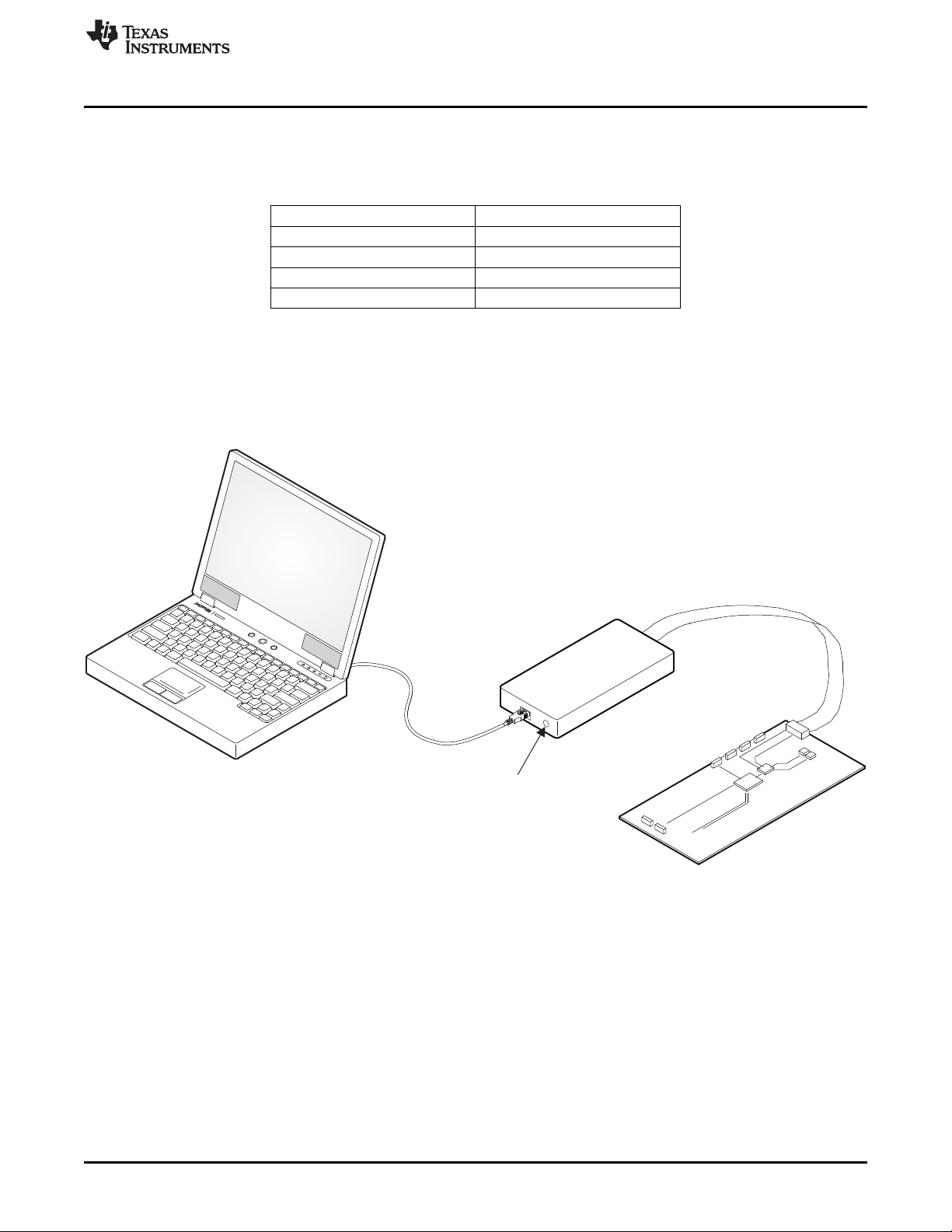
Host
Computer
USBCable
USB
Interface
Adapter
GreenLED
Indicates
Power
10-Pin
Ribbon
Cable
EVMBoard
USBInterface AdaptorQuickConnectionDiagram
www.ti.com
2.3 Hardware Setup
Table 2 shows the board default jumper settings.
Connect the USB-TO-GPIO adapter to your PC using the supplied USB cable. Connect the
TPS6236xEVM connector J8 to the USB-TO-GPIO adapter using the supplied 10-pin ribbon cable. The
connectors on the ribbon cable are keyed to prevent incorrect installation.
Setup
Table 2. Default Jumper Settings
JUMPER DEFAULT
JP1 Installed across pins 1 and 2
JP2 Installed across pins 2 and 3
JP3 Installed across pins 2 and 3
JP4 Installed across pins 1 and 2
Connect the load (processor) to either the output headers J4 and J6 (for currents below 1A) or to the
output terminal block J7 (for currents greater than 1A). The leads should be short and twisted.
Connect the SNS+ and SNS- signals from header J5 to the load. For proper regulation, these must be
connected to the output.
Install jumpers, JP1 through JP4 to the desired positions. Jumper JP1 must be across pins 1 and 2 for the
TPS6236x to operate.
Connect at least a 3 A rated input power supply, set to provide between 2.5V and 5.5V, between J1 and
J3. The leads should be short and twisted. Turn on the power supply.
SLVU425A–April 2011– Revised July 2011 TPS6236xEVM-655
Submit Documentation Feedback
Copyright © 2011, Texas Instruments Incorporated
5
Page 6
Software Setup and Operation
3 Software Setup and Operation
This section provides descriptions of the EVM software and functionality.
The supplied software is used to communicate with the TPS6236xEVM. Click on the icon on the host PC
to start the software. The host PC software first checks the firmware version of the USB-TO-GPIO
adapter. If an incorrect firmware version is installed, the software automatically searches on the Internet (if
connected) for updates. If a new update is available, the software notifies the user of the update,
downloads and installs the software. Note that after the firmware is updated, the user must disconnect and
then reconnect the USB cable between the adapter and PC, as instructed during the install process. The
host PC software also automatically searches on the Internet (if connected) for updates to the EVM
software. If a new update is available, the software notifies the user of the update, downloads and installs
the update.
VINand VDDmust be supplied for the software to detect the TPS6236x and run.
The software reads the registers on the TPS6236x and automatically determines which version of the IC is
installed. Even if the IC is disabled via the EN pin (JP4), the user can still communicate with the
TPS6236x if VINand VDDare supplied. If no IC is detected, the software will abort loading.
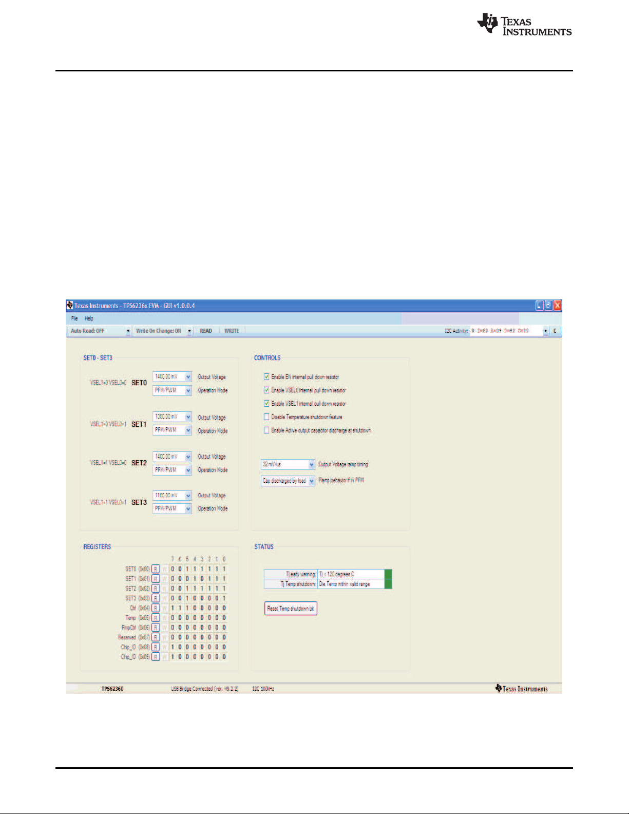
The software displays the main panel for the user interface, shown in Figure 1.
www.ti.com
Figure 1. TPS6236x Software Main Panel
6
TPS6236xEVM-655 SLVU425A–April 2011– Revised July 2011
Copyright © 2011, Texas Instruments Incorporated
Submit Documentation Feedback
Page 7

www.ti.com
It is recommended that the user press the 'READ' button at the top of the screen immediately after loading
the software to confirm that the software and cable connections are working properly. The message box at
the top right of the main panel (I2C Activity) displays all I2C activity. The message box at the bottom (USB
Bridge Connected) displays whether or not the USB-TO-GPIO connection is functional.
The software itself performs no calculations or computations and simply reads and writes to and from the
IC's registers through the I2C interface. Each register's bits can either be changed manually by changing
the boxes corresponding to each bit in the panel's bottom left half (REGISTERS section), or they can be
changed through the drop-down boxes and buttons in the rest of the panel. Some bits are reserved and
not writeable. These will not allow you to click on them to change their setting. For example, since the
TPS62360 does not have an operational register bit at bit 6 of registers 0x00h through 0x03h, the
TPS62360's main panel will not allow writes to those bits. The I2C bus speed is fixed at 100 kbps and this
is noted at the bottom of the screen.
Following any change to an individual bit, drop-down box, or button, the user must write the new values to
the registers by either clicking the 'W' button to the left of each affected register or by clicking the 'WRITE'
button at the top of the screen.
In order to reduce the amount of manual reading and writing required, the two drop-downs at the top left of
the screen have been provided to do this automatically. The 'Auto Read' drop down allows the option of
automatically reading all the registers at specific time intervals. The 'Write On Changes' drop-down allows
the option of automatically writing a change to the registers as soon as it is made in the software.
The TPS6236x datasheet is available via the 'Help' menu (Internet access is required). The datasheet
discusses the functionality of the various register bits, which is also briefly repeated here.
The drop-downs in the top left section of the software (SET0-SET3 section) correspond to registers 0x00h
thought 0x03h in the TPS6236x. These registers set the target output voltage and operating mode
(PFM/PWM or forced PWM). The output voltage on the TPS62360/2 is settable in 10 mV steps between
0.77V and 1.4V. The output voltage on the TPS62361B/5 is settable in 10 mV steps between 0.5V and
1.77V. The operating mode is either PFM/PWM, in which the IC is allowed to skip switching pulses at light
loads to keep the converting efficiency high, or forced PWM mode, in which the IC allows negative
inductor current at light loads to maintain a specific switching frequency and output noise. The TPS6236x
only runs at the settings of one of these four registers at a time. This operating register is selected by the
VSEL0 and VSEL1 jumpers and can be changed during operation.
The top right section of the software (CONTROLS section) contains the functionality of registers 0x04h
and 0x06h and some of the functionality of register 0x05h. The first 3 check boxes enable an internal
resistor on any of the EN, VSEL0, or VSEL1 pins. This resistor, which is internal to the TPS6236x, would
keep that pin in a defined state if it were left floating. The 'Disable Temperature shutdown feature' bit
disables the temperature shutdown internal to the IC, if selected. The 'Enable Active output capacitor
discharge at shutdown' forces the IC to actively discharge the output capacitor during shutdown. The first
drop-down sets the output voltage ramp timing and the final drop-down describes the ramp behavior when
the TPS6236x is changing its output voltage in PFM mode.
The bottom right section of the software (STATUS section) contains the remaining bits in register 0x05h.
The top indicator is green if the IC die temperature is low enough and turns red when the bit is set
corresponding to a die temperature exceeding 120°C typical. The indicator on the bottom turns red if
thermal shutdown has occurred. When this does occur, the TPS6236x will latch off and the temperature
must decrease below a hysteresis amount and the TJTemp shutdown bit needs to be reset by the user.
The button at the bottom of this section is provided for this purpose.
Software Setup and Operation
SLVU425A–April 2011– Revised July 2011 TPS6236xEVM-655
Submit Documentation Feedback
Copyright © 2011, Texas Instruments Incorporated
7
Page 8

Circuit Use and Modifications
4 Circuit Use and Modifications
Besides the required circuitry to operate the TPS6236x (outlined in a white silk screen border on the
PCB), there are additional circuits present on the TPS6236xEVM-655 that assist in evaluating the
TPS6236x as a processor power supply solution. Additionally, there are modifications that can be made to
adapt the circuit's performance to the needs of a particular application.
4.1 Load Step Circuit
The TPS6236xEVM-655 contains a simple circuit that can produce fast load current steps at the output of
the TPS6236x. This can evaluate the response of the TPS6236x to various load transients. To operate
this circuit, connect a function generator to SMA connector J10 or TP4. The output of the function
generator should be a square wave with a small duty cycle. The output high level controls the gate to
source voltage of the power transistor, Q1, and should be adjusted to generate the desired step current
high level. The output low level sets the step current low level. Good settings to start with are a square
wave signal running at 100 Hz and 5% duty cycle going from 0V to 1.5V. These settings can be adjusted
in order to generate the desired load step.
Resistor R6 is present to observe the load step current by measuring the voltage across TP2 and TP3.
Oscilloscope settings of 100mV / div translate to a current in R6 of 1A / div.
4.2 Output Voltage Buffer
The output voltage buffer circuit simply buffers the SNS+/- output with a unity gain op amp. This
transforms SNS+ and SNS- to a lower impedance signal that can be measured by high impedance
measurement equipment, such as an oscilloscope. The op amp, U2, is powered from the USB-TO-GPIO
adaptor. The USB-TO-GPIO adaptor must be installed for the output voltage buffer circuit to operate.
C13 is provided to reduce the bandwidth and noise of the input signal to the operational amplifier.
www.ti.com
4.3 Circuit Modifications
Modifications may be made to the circuit. Any modifications will affect the performance of the EVM and
must remain within the limits of the TPS6236x IC, as detailed in the datasheet.
4.3.1 Output Capacitors
There are 3 locations for extra output capacitors to be installed in order to reduce output ripple or lessen
the voltage drop due to a load transient. C7 allows an extra capacitor to be installed near the TPS6236x
IC, while C10 and C11 allow extra capacitors to be installed closer to the point of load, which is simulated
by the load step circuit. The total output capacitance must remain below the maximum capacitance
allowed in the datasheet.
4.3.2 Input Capacitors
C9 is provided to locate additional input capacitance near the TPS6236x input. Additional capacitance at
C9 will decrease the input voltage ripple.
C8 is provided to form a complete 'PI'-type filter for the AVIN input. With the change of R1 to some small
value (around 10 Ω), the C-R-C filter is complete. This filter is not necessary for operation of the
TPS6236x.
4.3.3 I2C Pull-up Resistors
R2 and R3 are locations for optional pull-up resistors for the I2C signals. They are required when not using
the USB-TO-GPIO adaptor but are not recommended when using the adaptor. If used, their typical value
is around 2.2kΩ.
8
TPS6236xEVM-655 SLVU425A–April 2011– Revised July 2011
Copyright © 2011, Texas Instruments Incorporated
Submit Documentation Feedback
Page 9

80
82
84
86
88
90
92
94
96
98
100
2.5 3 3.5 4 4.5 5 5.5
V - Input Voltage - V
I
Efficiency - %
0
10
20
30
40
50
60
70
80
90
100
0.1 1 10 100 1k 10k
I - Load Current - mA
O
0.92 V
1.4 V
1.7 V
1.16 V
Efficiency - %
www.ti.com
5 Test Results
This section provides typical performance waveforms for the TPS6236xEVM-655.
Test Results
Figure 2. Efficiency vs. Input Voltage (I
Figure 3. Efficiency vs. Output Current (VIN= 3.6V, V
= 1.5A, V
OUT
= 1.4V)
OUT
= 0.92, 1.16, 1.4, 1.7)
OUT
SLVU425A–April 2011– Revised July 2011 TPS6236xEVM-655
Submit Documentation Feedback
9
Copyright © 2011, Texas Instruments Incorporated
Page 10

-0.15
-0.1
-0.05
0
0.05
0.1
0.15
0.1 1 10 100 1k 10k
I - Load Current - mA
O
Load Regulation - %
-0.1
-0.08
-0.06
-0.04
-0.02
0
0.02
0.04
0.06
0.08
0.1
2.5 3 3.5 4 4.5 5 5.5
V - Input Voltage - V
I
Line Regulation - %
Test Results
www.ti.com
Figure 4. Load Regulation (V
Figure 5. Line Regulation (V
= 1.4V, VIN= 3.6V)
OUT
= 1.4V, I
OUT
OUT
= 1.5A)
10
TPS6236xEVM-655 SLVU425A–April 2011– Revised July 2011
Copyright © 2011, Texas Instruments Incorporated
Submit Documentation Feedback
Page 11

t - Time - 20 s/divm
0.5 A/div
0.5 V/div
5 V/div
EN
V
OUT
I
inductor
t - Time - 2 ms/div
0.5 V/div
5 V/div
0.5 A/div
EN
V
OUT
I
inductor
www.ti.com
Test Results
Figure 6. Start-up (VIN= 3.6V, V
Figure 7. Shutdown (VIN= 3.6V, V
OUT
= 1.4V, I
= 1.4V, I
OUT
= 0, output cap discharge enabled)
OUT
OUT
= 1.5A)
SLVU425A–April 2011– Revised July 2011 TPS6236xEVM-655
Submit Documentation Feedback
Copyright © 2011, Texas Instruments Incorporated
11
Page 12

t - Time - 200 ns/div
0.5 A/div
20 mV/div
5 V/div
SW
I
inductor
V (AC COUPLED)
OUT
t - Time - 200 ns/div
0.5 A/div
50 mV/div
5 V/div
SW
I
inductor
V (AC COUPLED)
IN
Test Results
www.ti.com
Figure 8. Output Voltage Ripple (VIN= 3.6V, V
Figure 9. Input Voltage Ripple (VIN= 3.6V, V
OUT
OUT
= 1.4V, I
= 1.4V, I
OUT
OUT
= 3A)
= 3A)
12
TPS6236xEVM-655 SLVU425A–April 2011– Revised July 2011
Copyright © 2011, Texas Instruments Incorporated
Submit Documentation Feedback
Page 13

t - Time - 5 s/divm
50 mV/div
1 A/div
I
1A to 2A load Step
OUT
V (AC COUPLED)
OUT
www.ti.com
Test Results
Figure 10. Load Transient Response (VIN= 3.6V, V
OUT
= 1.4V, I
= 1A to 2A step)
OUT
Figure 11. Thermal Performance (VIN= 3.6V, V
OUT
= 1.4V, I
OUT
= 3A)
SLVU425A–April 2011– Revised July 2011 TPS6236xEVM-655
Submit Documentation Feedback
Copyright © 2011, Texas Instruments Incorporated
13
Page 14

Board Layout
6 Board Layout
This section provides the TPS6236xEVM-655 board layout and illustrations.
Board layout is critical for all high-frequency, switch-mode power supplies. Figure 12 through Figure 15
show the board layout for the TPS6236xEVM-655 PCB. The nodes with high-switching frequencies and
currents are kept as short as possible to minimize trace inductance. Careful attention has been given to
the routing of high-frequency current loops and a single-point grounding scheme is used. Also, the
majority of the heatsinking for this device occurs through the top layer traces and vias pulled from the IC's
solder bumps that carry high currents. See the data sheet for specific layout guidelines.
www.ti.com
14
Figure 12. Assembly Layer
TPS6236xEVM-655 SLVU425A–April 2011– Revised July 2011
Copyright © 2011, Texas Instruments Incorporated
Submit Documentation Feedback
Page 15

www.ti.com
Board Layout
Figure 13. Top Layer
Figure 14. Layer 2
SLVU425A–April 2011– Revised July 2011 TPS6236xEVM-655
Submit Documentation Feedback
Copyright © 2011, Texas Instruments Incorporated
15
Page 16

Board Layout
www.ti.com
Figure 15. Layer 3
16
Figure 16. Bottom Layer
TPS6236xEVM-655 SLVU425A–April 2011– Revised July 2011
Copyright © 2011, Texas Instruments Incorporated
Submit Documentation Feedback
Page 17

www.ti.com
7 Schematic and Bill of Materials
This section provides the TPS6236xEVM-655 schematic and bill of materials. The bill of materials is provided in two tables. Table 3 are the
components required to build the TPS6236x solution. Table 4 are the components used only to evaluate the TPS6236xEVM-655 solution.
7.1 Schematic
Schematic and Bill of Materials
Figure 17. TPS6236xEVM-655 Schematic
SLVU425A–April 2011– Revised July 2011 TPS6236xEVM-655
Submit Documentation Feedback
Copyright © 2011, Texas Instruments Incorporated
17
Page 18

Schematic and Bill of Materials
7.2 Bill of Materials
www.ti.com
Table 3. TPS6236x Solution Required Components
Count
-001 -002 -003 -004
3 3 3 3 C1, C4, C5 0.1 µF Capacitor, Ceramic, 10V, X5R, 20% 0402 Std Std
2 2 2 2 C2, C6 10 µF Capacitor, Ceramic, 6.3V, X5R, 20% 0603 Std Std
1 1 1 1 L1 1.0 µH Inductor, Power, 5.4 A, 10.8 mΩ, ±20% 0.157 x 0.157 inch XFL4020-102ME Coilcraft
1 0 0 0 U1 TPS62360YZH IC, 3A Processor Supply Converter BGA TPS62360YZH TI
0 1 0 0 U1 TPS62361BYZH IC, 3A Processor Supply Converter BGA TPS62361BYZH TI
0 0 1 0 U1 TPS62362YZH IC, 3A Processor Supply Converter BGA TPS62362YZH TI
0 0 0 1 U1 TPS62365YZH IC, 3.5A Processor Supply Converter BGA TPS62365YZH TI
RefDes Value Description Size Part Number MFR
Table 4. TPS6236xEVM-655 Evaluation Components
Count
-001 -002 -003 -004
1 1 1 1 C12 0.1 µF Capacitor, Ceramic, 10V, X5R, 20% 0402 Std Std
1 1 1 1 C3 100 µF Capacitor, Ceramic, 6.3V, X5R, 20% 1210 Std Std
0 0 0 0 C7, C10, C11 Open Capacitor, Ceramic, 6.3V, X5R, 20% 0805 Std Std
0 0 0 0 C8, C9 Open Capacitor, Ceramic, 6.3V, X5R, 20% 0603 Std Std
0 0 0 0 C13 Open Capacitor, Ceramic, 25V, X7R, 10% 0603 Std Std
1 1 1 1 Q1 IRLR3715 MOSFET, N-ch, 20V, 49A, 11 mΩ DPAK IRLR3715ZCPBF IR
1 1 1 1 R1 0 Resistor, Chip, 1/10W 0603 Std Std
0 0 0 0 R2, R3 Open Resistor, Chip, 1/16W, 1% 0603 Std Std
2 2 2 2 R4, R5 10 Resistor, Chip, 1/16W, 1% 0603 Std Std
1 1 1 1 R6 0.1 Resistor, Chip, 1W, 1% 2512 Std Std
1 1 1 1 R7 100 Resistor, Chip, 1/16W, 1% 0603 Std Std
5 5 5 5 R8, R9, R10, R11, 10.0K Resistor, Chip, 1/16W, 1% 0603 Std Std
1 1 1 1 U2 OPA334 IC, 0.05 µV/°C Max, Single Supply Op Amp, Zero-Drift SOT23-6 OPA334AIDBV TI
RefDes Value Description Size Part Number MFR
R12
7.3 Related Documentation From Texas Instruments
Processor Supply with I2C Compatible Interface and Remote Sense data sheet (SLVSAU9)
18
TPS6236xEVM-655 SLVU425A–April 2011– Revised July 2011
Copyright © 2011, Texas Instruments Incorporated
Submit Documentation Feedback
Page 19

Evaluation Board/Kit Important Notice
Texas Instruments (TI) provides the enclosed product(s) under the following conditions:
This evaluation board/kit is intended for use for ENGINEERING DEVELOPMENT, DEMONSTRATION, OR EVALUATION
PURPOSES ONLY and is not considered by TI to be a finished end-product fit for general consumer use. Persons handling the
product(s) must have electronics training and observe good engineering practice standards. As such, the goods being provided are
not intended to be complete in terms of required design-, marketing-, and/or manufacturing-related protective considerations,
including product safety and environmental measures typically found in end products that incorporate such semiconductor
components or circuit boards. This evaluation board/kit does not fall within the scope of the European Union directives regarding
electromagnetic compatibility, restricted substances (RoHS), recycling (WEEE), FCC, CE or UL, and therefore may not meet the
technical requirements of these directives or other related directives.
Should this evaluation board/kit not meet the specifications indicated in the User’s Guide, the board/kit may be returned within 30
days from the date of delivery for a full refund. THE FOREGOING WARRANTY IS THE EXCLUSIVE WARRANTY MADE BY
SELLER TO BUYER AND IS IN LIEU OF ALL OTHER WARRANTIES, EXPRESSED, IMPLIED, OR STATUTORY, INCLUDING
ANY WARRANTY OF MERCHANTABILITY OR FITNESS FOR ANY PARTICULAR PURPOSE.
The user assumes all responsibility and liability for proper and safe handling of the goods. Further, the user indemnifies TI from all
claims arising from the handling or use of the goods. Due to the open construction of the product, it is the user’s responsibility to
take any and all appropriate precautions with regard to electrostatic discharge.
EXCEPT TO THE EXTENT OF THE INDEMNITY SET FORTH ABOVE, NEITHER PARTY SHALL BE LIABLE TO THE OTHER
FOR ANY INDIRECT, SPECIAL, INCIDENTAL, OR CONSEQUENTIAL DAMAGES.
TI currently deals with a variety of customers for products, and therefore our arrangement with the user is not exclusive.
TI assumes no liability for applications assistance, customer product design, software performance, or infringement of
patents or services described herein.
Please read the User’s Guide and, specifically, the Warnings and Restrictions notice in the User’s Guide prior to handling the
product. This notice contains important safety information about temperatures and voltages. For additional information on TI’s
environmental and/or safety programs, please contact the TI application engineer or visit www.ti.com/esh.
No license is granted under any patent right or other intellectual property right of TI covering or relating to any machine, process, or
combination in which such TI products or services might be or are used.
FCC Warning
This evaluation board/kit is intended for use for ENGINEERING DEVELOPMENT, DEMONSTRATION, OR EVALUATION
PURPOSES ONLY and is not considered by TI to be a finished end-product fit for general consumer use. It generates, uses, and
can radiate radio frequency energy and has not been tested for compliance with the limits of computing devices pursuant to part 15
of FCC rules, which are designed to provide reasonable protection against radio frequency interference. Operation of this
equipment in other environments may cause interference with radio communications, in which case the user at his own expense
will be required to take whatever measures may be required to correct this interference.
EVM Warnings and Restrictions
It is important to operate this EVM within the input voltage range of 2.5 V to 5.5 V and the output voltage range of 0.5 V to 1.77 V .
Exceeding the specified input range may cause unexpected operation and/or irreversible damage to the EVM. If there are
questions concerning the input range, please contact a TI field representative prior to connecting the input power.
Applying loads outside of the specified output range may result in unintended operation and/or possible permanent damage to the
EVM. Please consult the EVM User's Guide prior to connecting any load to the EVM output. If there is uncertainty as to the load
specification, please contact a TI field representative.
During normal operation, some circuit components may have case temperatures greater than 85°C. The EVM is designed to
operate properly with certain components above 85°C as long as the input and output ranges are maintained. These components
include but are not limited to linear regulators, switching transistors, pass transistors, and current sense resistors. These types of
devices can be identified using the EVM schematic located in the EVM User's Guide. When placing measurement probes near
these devices during operation, please be aware that these devices may be very warm to the touch.
Mailing Address: Texas Instruments, Post Office Box 655303, Dallas, Texas 75265
Copyright © 2011, Texas Instruments Incorporated
Page 20

IMPORTANT NOTICE
Texas Instruments Incorporated and its subsidiaries (TI) reserve the right to make corrections, modifications, enhancements, improvements,
and other changes to its products and services at any time and to discontinue any product or service without notice. Customers should
obtain the latest relevant information before placing orders and should verify that such information is current and complete. All products are
sold subject to TI’s terms and conditions of sale supplied at the time of order acknowledgment.
TI warrants performance of its hardware products to the specifications applicable at the time of sale in accordance with TI’s standard
warranty. Testing and other quality control techniques are used to the extent TI deems necessary to support this warranty. Except where
mandated by government requirements, testing of all parameters of each product is not necessarily performed.
TI assumes no liability for applications assistance or customer product design. Customers are responsible for their products and
applications using TI components. To minimize the risks associated with customer products and applications, customers should provide
adequate design and operating safeguards.
TI does not warrant or represent that any license, either express or implied, is granted under any TI patent right, copyright, mask work right,
or other TI intellectual property right relating to any combination, machine, or process in which TI products or services are used. Information
published by TI regarding third-party products or services does not constitute a license from TI to use such products or services or a
warranty or endorsement thereof. Use of such information may require a license from a third party under the patents or other intellectual
property of the third party, or a license from TI under the patents or other intellectual property of TI.
Reproduction of TI information in TI data books or data sheets is permissible only if reproduction is without alteration and is accompanied
by all associated warranties, conditions, limitations, and notices. Reproduction of this information with alteration is an unfair and deceptive
business practice. TI is not responsible or liable for such altered documentation. Information of third parties may be subject to additional
restrictions.
Resale of TI products or services with statements different from or beyond the parameters stated by TI for that product or service voids all
express and any implied warranties for the associated TI product or service and is an unfair and deceptive business practice. TI is not
responsible or liable for any such statements.
TI products are not authorized for use in safety-critical applications (such as life support) where a failure of the TI product would reasonably
be expected to cause severe personal injury or death, unless officers of the parties have executed an agreement specifically governing
such use. Buyers represent that they have all necessary expertise in the safety and regulatory ramifications of their applications, and
acknowledge and agree that they are solely responsible for all legal, regulatory and safety-related requirements concerning their products
and any use of TI products in such safety-critical applications, notwithstanding any applications-related information or support that may be
provided by TI. Further, Buyers must fully indemnify TI and its representatives against any damages arising out of the use of TI products in
such safety-critical applications.
TI products are neither designed nor intended for use in military/aerospace applications or environments unless the TI products are
specifically designated by TI as military-grade or "enhanced plastic." Only products designated by TI as military-grade meet military
specifications. Buyers acknowledge and agree that any such use of TI products which TI has not designated as military-grade is solely at
the Buyer's risk, and that they are solely responsible for compliance with all legal and regulatory requirements in connection with such use.
TI products are neither designed nor intended for use in automotive applications or environments unless the specific TI products are
designated by TI as compliant with ISO/TS 16949 requirements. Buyers acknowledge and agree that, if they use any non-designated
products in automotive applications, TI will not be responsible for any failure to meet such requirements.
Following are URLs where you can obtain information on other Texas Instruments products and application solutions:
Products Applications
Audio www.ti.com/audio Communications and Telecom www.ti.com/communications
Amplifiers amplifier.ti.com Computers and Peripherals www.ti.com/computers
Data Converters dataconverter.ti.com Consumer Electronics www.ti.com/consumer-apps
DLP® Products www.dlp.com Energy and Lighting www.ti.com/energy
DSP dsp.ti.com Industrial www.ti.com/industrial
Clocks and Timers www.ti.com/clocks Medical www.ti.com/medical
Interface interface.ti.com Security www.ti.com/security
Logic logic.ti.com Space, Avionics and Defense www.ti.com/space-avionics-defense
Power Mgmt power.ti.com Transportation and www.ti.com/automotive
Microcontrollers microcontroller.ti.com Video and Imaging www.ti.com/video
RFID www.ti-rfid.com Wireless www.ti.com/wireless-apps
RF/IF and ZigBee® Solutions www.ti.com/lprf
TI E2E Community Home Page e2e.ti.com
Automotive
Mailing Address: Texas Instruments, Post Office Box 655303, Dallas, Texas 75265
Copyright © 2011, Texas Instruments Incorporated
Page 21

Mouser Electronics
Authorized Distributor
Click to View Pricing, Inventory, Delivery & Lifecycle Information:
Texas Instruments:
TPS62360EVM-655 TPS62361BEVM-655 TPS62362EVM-655
 Loading...