

Texas Instruments TPS62220DDC, TPS62221DDC, TPS62222DDC, TPS62223DDC, TPS62224DDC Schematic [ru]
...
www.ti.com
V
I
GND
ENSWFB
C3
4.7 Fm
L1
4.7 Hm
C4
10 Fm
TPS62220
V
I
2.5 V to 6 V
V
O
1.5 V/400 mA
R1
360 kW
R2
180 kW
C1
22 pF
C2
100 pF
1
2
3
5
4
40
45
50
55
60
65
70
75
80
85
90
95
100
0.01 0.1 1 10 100 1000
VO= 1.8 V,
L = 4.7 H,m
CO= 22 Fm
Efficency − %
IL− Load Current − mA
VI= 3.7 V
Typical Application (Adjustible Output Voltage Version)
VI= 5 V
VI= 2.7 V
400-mA, 1.25-MHz, HIGH-EFFICIENCY, STEP-DOWN CONVERTER IN THIN-SOT23
FEATURES DESCRIPTION
• High-Efficiency Synchronous Step-Down
Converter With up to 95% Efficiency
• 2.5-V to 6-V Input Voltage Range
• Adjustable Output Voltage Range From 0.7 V
to V
I
• Fixed Output Voltage Options Available
• Up to 400-mA Output Current
• 1.25-MHz Fixed Frequency PWM Operation
• Highest Efficiency Over Wide Load Current
Range Due to Power-Save Mode
• 15-µA Typical Quiescent Current
• Soft Start
• 100% Duty Cycle Low-Dropout Operation
• Dynamic Output-Voltage Positioning
• Available in TSOT23 Package
APPLICATIONS
• PDAs and Pocket PC
• Cellular Phones, Smart Phones
• OMAP™ and Low Power DSP Supply
• Digital Cameras
• Portable Media Players
• Portable Equipment
• WLAN PC Cards
The TPS6222x devices are a family of high-efficiency,
synchronous step-down converters ideally suited for
portable systems powered by 1-cell Li-Ion or 3-cell
NiMH/NiCd batteries. The devices are also suitable to
operate from a standard 3.3-V or 5-V voltage rail.
With an output voltage range of 6 V down to 0.7 V
and up to 400-mA output current, the devices are
ideal for powering the low voltage TMS320™ DSP
family and processors used in PDAs, pocket PCs,
and smart phones. Under nominal load current, the
devices operate with a fixed switching frequency of
typically 1.25 MHz. At light load currents, the part
enters the power-save mode operation; the switching
frequency is reduced and the quiescent current is
typically only 15 µA; therefore, the device achieves
the highest efficiency over the entire load current
range. The TPS6222x needs only three small
external components. Together with the tiny TSOT23
package, a minimum system solution size can be
achieved. An advanced fast response voltage mode
control scheme achieves superior line and load
regulation with small ceramic input and output
capacitors.
TPS62220, TPS62221, TPS62222
TPS62223, TPS62224, TPS62227
TPS62228, TPS62229
SLVS491D – SEPTEMBER 2003 – REVISED MARCH 2006
OMAP, TMS320 are trademarks of Texas Instruments.
PRODUCTION DATA information is current as of publication date.
Products conform to specifications per the terms of the Texas
Instruments standard warranty. Production processing does not
necessarily include testing of all parameters.
Please be aware that an important notice concerning availability, standard warranty, and use in critical applications of Texas
Instruments semiconductor products and disclaimers thereto appears at the end of this data sheet.
Copyright © 2003–2006, Texas Instruments Incorporated
www.ti.com
TPS62220, TPS62221, TPS62222
TPS62223, TPS62224, TPS62227
TPS62228, TPS62229
SLVS491D – SEPTEMBER 2003 – REVISED MARCH 2006
These devices have limited built-in ESD protection. The leads should be shorted together or the device placed in conductive foam
during storage or handling to prevent electrostatic damage to the MOS gates.
ORDERING INFORMATION
T
A
OUTPUT VOLTAGE THIN-SOT23 PACKAGE SYMBOL
(1)
Adjustable TPS62220DDC ALN
1.5 V TPS62221DDC ALO
1.6 V TPS62224DDC ALQ
-40°C to 85°C
1.7 V TPS62229DDC EJ
1.8 V TPS62222DDC APP
1.875 V TPS62228DDC EH
2.3 V TPS62223DDC ALX
1.2 V TPS62227DDC BRZ
(1) The DDC package is available in tape and reel. Add R suffix (TPS62220DDCR) to order quantities of 3000 parts. Add T suffix
(TPS62220DDCT) to order quantities of 250 parts.
ABSOLUTE MAXIMUM RATINGS
over operating free-air temperature (unless otherwise noted)
V
I
Supply voltage on pin
Voltages on pins SW, EN, FB
P
D
T
J
T
stg
Continuous power dissipation See Dissipation Rating Table
Operating junction temperature range -40 to 150 °C
Storage temperature -65 to 150 °C
Lead temperature (soldering, 10 sec) 260 °C
(1) Stresses beyond those listed under "absolute maximum ratings” may cause permanent damage to the device. These are stress ratings
only, and functional operation of the device at these or any other conditions beyond those indicated under "recommended operating
conditions” is not implied. Exposure to absolute-maximum-rated conditions for extended periods may affect device reliability.
(2) All voltage values are with respect to network ground terminal.
(2)
(2)
(1)
TPS6222x UNIT
-0.3 to 7.0 V
-0.3 to VI+0.3 V
DISSIPATION RATING TABLE
PACKAGE
TA≤ 25°C DERATING FACTOR TA= 70°C TA= 85°C
POWER RATING ABOVE TA= 25°C POWER RATING POWER RATING
(1)
DDC 400 mW 4 mW/°C 220 mW 160 mW
(1) The thermal resistance junction to ambient of the 5-pin Thin-SOT23 is 250°C/W.
RECOMMENDED OPERATING CONDITIONS
V
V
I
L Inductor
C
T
T
(1) See the application section for further information
2
Supply voltage 2.5 6 V
I
Output voltage range for adjustable output voltage version 0.7 V
O
Output current 400 mA
O
Input capacitor
I
Operating ambient temperature -40 85 °C
A
Operating junction temperature -40 125 °C
J
(1)
(1)
Submit Documentation Feedback
MIN NOM MAX UNIT
I
4.7 µH
4.7 µF
V
www.ti.com
TPS62220, TPS62221, TPS62222
TPS62223, TPS62224, TPS62227
TPS62228, TPS62229
SLVS491D – SEPTEMBER 2003 – REVISED MARCH 2006
ELECTRICAL CHARACTERISTICS
VI= 3.6 V, VO= 1.8 V, IO= 200 mA, EN = VIN, TA= -40 °C to 85 °C, typical values are at TA= 25 °C (unless otherwise noted)
PARAMETER TEST CONDITIONS MIN TYP MAX UNIT
SUPPLY CURRENT
V
I
I
Q
ENABLE
V
(EN)
I
(EN)
POWER SWITCH
r
DS(on)
I
lkg
I
(LIM)
OSCILLATOR
f
S
OUTPUT
I
O
V
O
V
ref
V
O
I
lkg
Input voltage range 2.5 6 V
Operating quiescent current IO= 0 mA, Device is not switching 15 25 µA
Shutdown supply current EN = GND 0.1 1 µA
Undervoltage lockout threshold 1.5 2 V
EN high level input voltage 1.3 V
EN low level input voltage 0.4 V
EN input bias current EN = GND or VIN 0.01 0.1 µA
P-channel MOSFET on-resistance m Ω
N-channel MOSFET on-resistance m Ω
VI= V
VI= V
VI= V
VI= V
P-channel leakage current V
N-channel leakage current V
= 3.6 V 530 670
GS
= 2.5 V 670 850
GS
= 3.6 V 430 540
GS
= 2.5 V 530 660
GS
= 6 V 0.1 1 µA
DS
= 6 V 0.1 1 µA
DS
P-channel current limit 2.5 V < VI< 6 V 600 670 880 mA
Switching frequency 0.8 1.25 1.85 MHz
Output current 400 mA
Adjustable output voltage
range
TPS62220 0.7 V
Reference voltage 0.5 V
Feedback voltage, See
Fixed output voltage
TPS62220
(1)
Adjustable
TPS62221
1.5 V
TPS62224
1.6 V
TPS62229
1.7 V
TPS62222
1.8 V
TPS62228
1.875 V
TPS62223
2.3 V
TPS62227
1.2 V
VI= 3.6 V to 6 V, IO= 0 mA 0% 3%
VI= 3.6 V to 6 V, 0 mA ≤ IO≤ 400 mA -3% 3%
VI= 2.5 V to 6 V, IO= 0 mA 0% 3%
VI= 2.5 V to 6 V, 0 mA ≤ IO≤ 400 mA -3% 3%
VI= 2.5 V to 6 V, IO= 0 mA 0% 3%
VI= 2.5 V to 6 V, 0 mA ≤ IO≤ 400 mA -3% 3%
VI= 2.5 V to 6 V, IO= 0 mA 0% 3%
VI= 2.5 V to 6 V, 0 mA ≤ IO≤ 400 mA -3% 3%
VI= 2.5 V to 6 V, IO= 0 mA 0% 3%
VI= 2.5 V to 6 V, 0 mA ≤ IO≤ 400 mA -3% 3%
VI= 2.5 V to 6 V, IO= 0 mA 0% 3%
VI= 2.5 V to 6 V, 0 mA ≤ IO≤ 400 mA -3% 3%
VI= 2.7 V to 6 V, IO= 0 mA 0% 3%
VI= 2.7 V to 6 V, 0 mA ≤ IO≤ 400 mA -3% 3%
VI= 2.7 V to 6 V, IO= 0 mA 0% 3%
VI= 2.7 V to 6 V, 0 mA ≤ IO≤ 400 mA -3% 3%
Line regulation VI= 2.5 V to 6 V, IO= 10 mA 0.26 %/V
Load regulation IO= 100 mA to 400 mA 0.0014 %/mA
Leakage current into SW pin VI> VO, 0 V ≤ V
Reverse leakage current into pin SW VI= open, EN = GND, V
≤ V
(SW)
I
= 6 V 0.1 1 µA
(SW)
0.1 1 µA
V
IN
(1) For output voltages ≤ 1.2 V, a 22-µF output capacitor value is required to achieve a maximum output voltage accuracy of 3% while
operating in power-save mode (PFM mode). For output voltages ≥ 2 V, an inductor of 10 µH and an output capacitor of ≥ 10 µF is
recommended. See the Application Information section for external components.
Submit Documentation Feedback
3
www.ti.com
3
2
4
5
1
V
I
GND
EN
SW
FB
TPS62220, TPS62221, TPS62222
TPS62223, TPS62224, TPS62227
TPS62228, TPS62229
SLVS491D – SEPTEMBER 2003 – REVISED MARCH 2006
PIN ASSIGNMENTS
DDC PACKAGE
(TOP VIEW)
Terminal Functions
TERMINAL
NAME NO.
EN 3 I This is the enable pin of the device. Pulling this pin to ground forces the device into shutdown mode.
FB 4 I This is the feedback pin of the device. Connect this pin directly to the output if the fixed output voltage
GND 2 Ground
SW 5 I/O Connect the inductor to this pin. This pin is the switch pin and is connected to the internal MOSFET
V
I
1 I Supply voltage pin
I/O DESCRIPTION
Pulling this pin to Vin enables the device. This pin must be terminated.
version is used. For the adjustable version, an external resistor divider is connected to this pin. The
internal voltage divider is disabled for the adjustable version.
switches.
4
Submit Documentation Feedback
www.ti.com
_
+
_
+
_
+
_
+
_
+
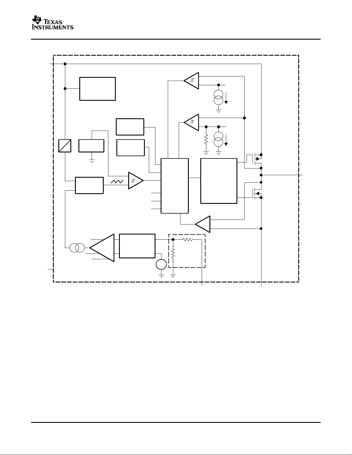
REF
REF
Load Comparator
Skip Comparator
Current Limit Comparator
P-Channel
Power MOSFET
Driver
Shoot-Through
Logic
Control
Logic
Soft Start
1.25 MHz
Oscillator
Comparator
S
R
N-Channel
Power MOSFET
Comparator High
Comparator Low
Comparator Low 2
V
(COMP)
Sawtooth
Generator
V
I
Undervoltage
Lockout
Bias Supply
_
+
Comparator High
Comparator Low
Comparator Low 2
Compensation
V
REF
= 0.5 V
R2
See Note
R1
V
I
EN
SW
FB GND
Gm
FUNCTIONAL BLOCK DIAGRAM
TPS62220, TPS62221, TPS62222
TPS62223, TPS62224, TPS62227
TPS62228, TPS62229
SLVS491D – SEPTEMBER 2003 – REVISED MARCH 2006
NOTE: For the adjustable version (TPS62220) the internal feedback divider is disabled, and the FB pin is directly connected
to the internal GM amplifier
Submit Documentation Feedback
5
www.ti.com
40
45
50
55
60
65
70
75
80
85
90
95
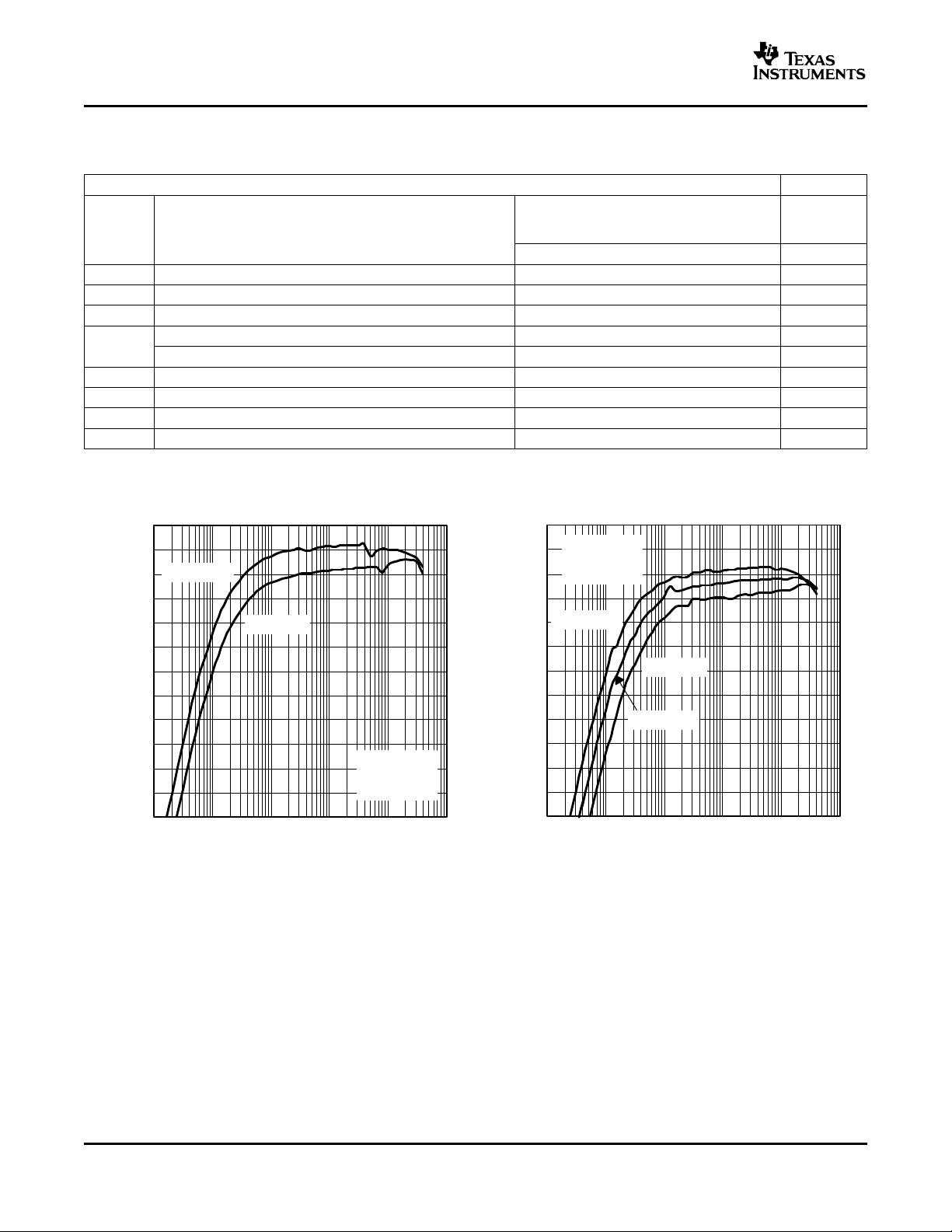
100
0.01 0.1 1 10 100 1000
VO = 3.3 V ,
L = 4.7 µH,
CO = 10 µF
VI = 3.7 V
VI = 5 V
Efficency - %
IL - Load Current - mA
40
45
50
55
60
65
70
75
80
85
90
95
100
0.01 0.1 1 10 100 1000
VO = 1.8 V ,
L = 4.7 µH,
CO = 22 µF
VI = 2.7 V
VI = 5 V
Efficency - %
IL - Load Current - mA
VI = 3.7 V
TPS62220, TPS62221, TPS62222
TPS62223, TPS62224, TPS62227
TPS62228, TPS62229
SLVS491D – SEPTEMBER 2003 – REVISED MARCH 2006
η Efficiency
I
Q
f
s
V
o
r
ds(on)
No load quiescent current vs Input voltage Figure 5
Switching frequency vs Temperature Figure 6
Output voltage vs Output current Figure 7
r
- P-channel switch, vs Input voltage Figure 8
ds(on)
r
- N-Channel rectifier switch vs Input voltage Figure 9
ds(on)
Load transient response Figure 10
PWM mode operation Figure 11
Power-save mode operation Figure 12
Start-up Figure 13
EFFICIENCY EFFICIENCY
vs vs
LOAD CURRENT LOAD CURRENT
TYPICAL CHARACTERISTICS
Table of Graphs
FIGURE
Figure 1 ,
vs Load current Figure 2 ,
Figure 3
vs Input voltage Figure 4
Figure 1. Figure 2.
6
Submit Documentation Feedback
www.ti.com
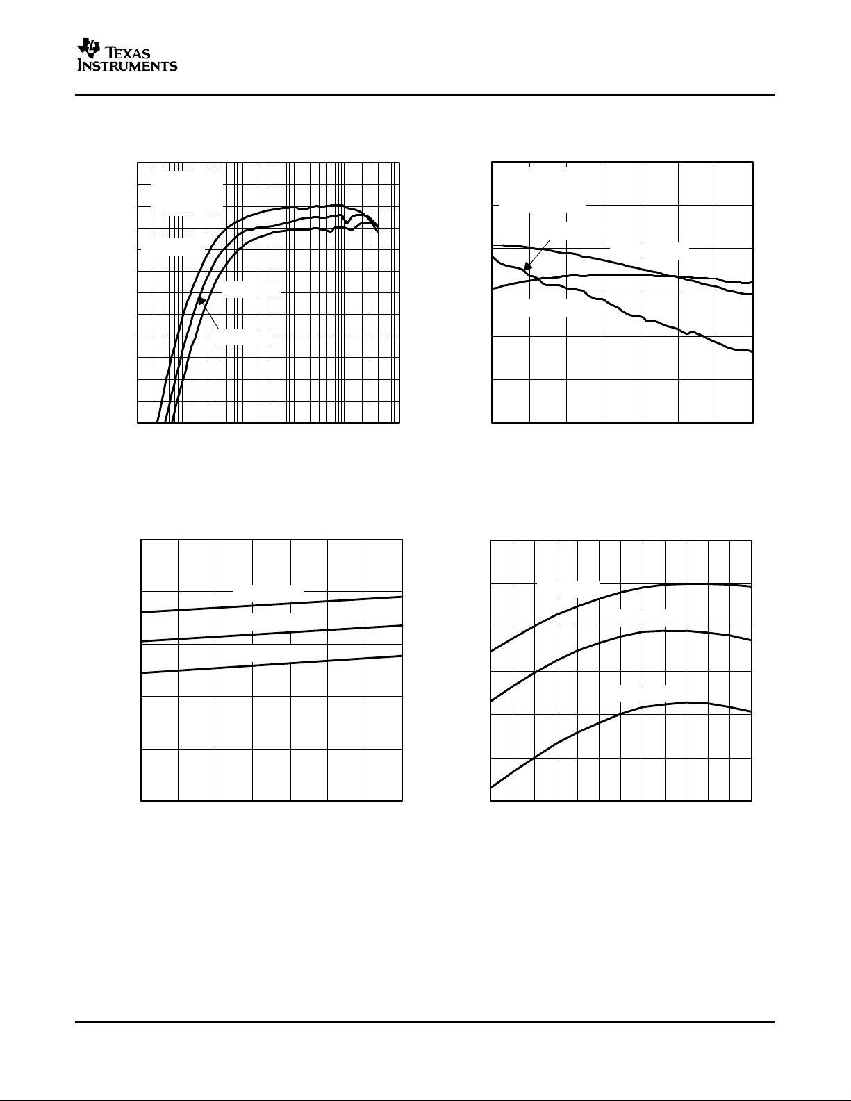
70
75
80
85
90
95
100
2.5 3 3.5 4 4.5 5 5.5 6
VO = 1.8 V ,
L = 4.7 µH,
CO = 22 µF
IL = 150 mA
IL = 300 mA
Efficiency − %
VI − Input Voltage − V
IL = 1 mA
40
45
50
55
60
65
70
75
80
85
90
95
100
0.01 0.1 1 10 100 1000
VO = 1.5 V ,
L = 4.7 µH,
CO = 10 µF
VI = 2.7 V
VI = 5 V
Efficency - %
IL - Load Current - mA
VI = 3.7 V
0
5
10
15
20
25
2.5 3 3.5 4 4.5 5 5.5 6
TA = 85°C
TA = 25°C
TA = −40°C
N0 Load Quiescent Current −
VI − Input Voltage − V
Aµ
1130
1140
1150
1160
1170
1180
1190
−40 −30 −20 −10 0 10 20 30 40 50 60 70 80
TA − Temperature − °C
VI = 3.6 V
VI = 6 V
VI = 2.5 V
f − Switching Frequency − kHz
TPS62220, TPS62221, TPS62222
TPS62223, TPS62224, TPS62227
SLVS491D – SEPTEMBER 2003 – REVISED MARCH 2006
EFFICIENCY EFFICIENCY
vs vs
LOAD CURRENT INPUT VOLTAGE
TPS62228, TPS62229
Figure 3. Figure 4.
NO LOAD QUIESCENT CURRENT SWITCHING FREQUENCY
INPUT VOLTAGE TEMPERATURE
Figure 5. Figure 6.
vs vs
Submit Documentation Feedback
7
www.ti.com
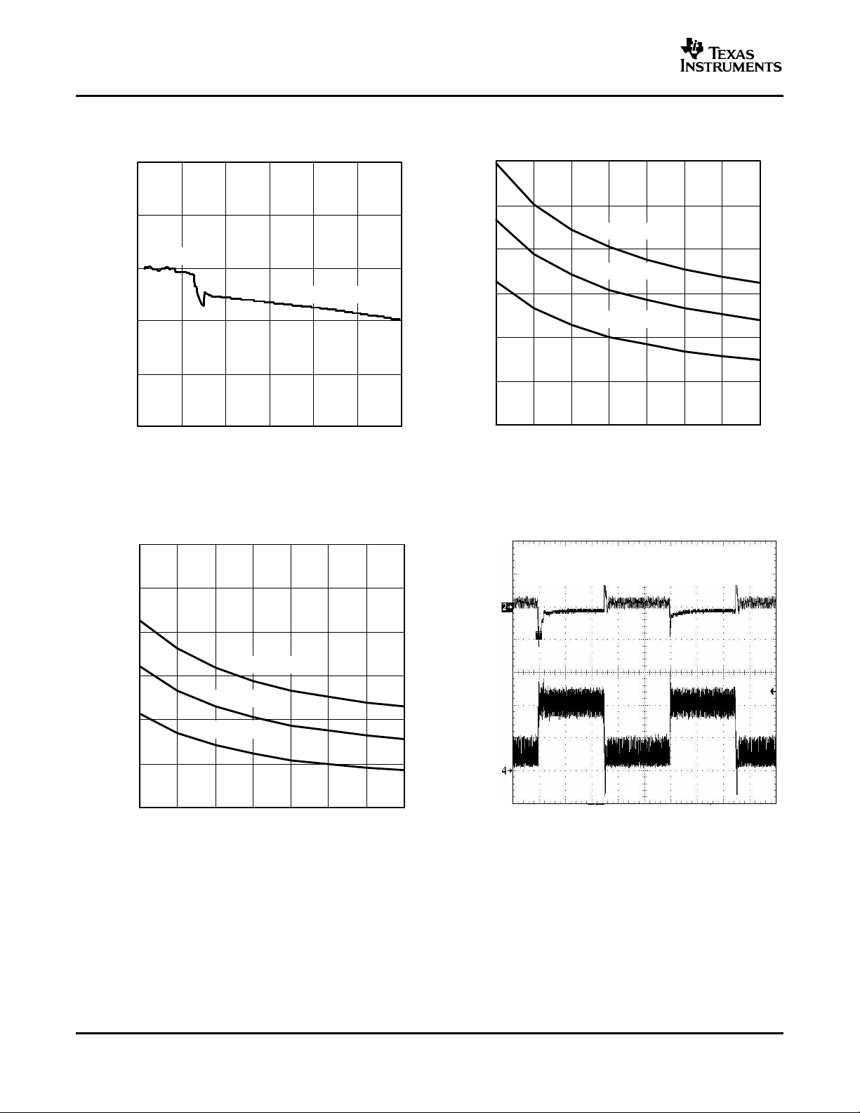
0.2
0.3
0.4
0.5
0.6
0.7
0.8
2.5 3 3.5 4 4.5 5 5.5 6
TA = 85°C
TA = 25°C
TA = -40°C
VI - Input Voltage - V
r
ds(on)
Ω- P-Channel Switch -
1.45
1.47
1.49
1.51
1.53
1.55
0 50 100 150 200 250 300
− Outrput Voltage − VV
O
IO − Output Current − mA
PFM Mode
PWM Mode
V
O
100 mV/div
I
L
200 mA/div
VI = 3.6 V , VO = 1.5 V , L = 4.7 µH,
CO =10 µF, Load Step 50 mA to 390 mA
transient
200 µs/div
0.2
0.3
0.4
0.5
0.6
0.7
0.8
2.5 3 3.5 4 4.5 5 5.5 6
TA = 85°C
TA = 25°C
TA = −40°C
VI − Input Voltage − V
rDS
(on)
ΩN-Channel Switch —
TPS62220, TPS62221, TPS62222
TPS62223, TPS62224, TPS62227
TPS62228, TPS62229
SLVS491D – SEPTEMBER 2003 – REVISED MARCH 2006
OUTPUT VOLTAGE r
OUTPUT CURRENT INPUT VOLTAGE
r
ds(on)
vs vs
Figure 7. Figure 8.
N-CHANNEL SWITCH LOAD TRANSIENT RESPONSE
vs
INPUT VOLTAGE
P-CHANNEL SWITCH
ds(on)
8
Figure 9. Figure 10.
Submit Documentation Feedback

www.ti.com
V
SW
5 V/div
V
O
20 mV/div
I
L
200 mA/div
VI = 3.6 V ,
VO = 1.5 V ,
IO = 400 mA
250 ns/div
VI = 3.6 V ,
VO = 1.5 V
VSW,
5 V/div
VO,
20 mV/div
IL,
200 mA/div
5 µs/div
Enable
2 V/div
V
O
1 V/div
I
i
200 mA/div
START-UP
250 µs/div
VI = 3.6 V ,
VO = 1.5 V ,
IO = 380 mA
TPS62220, TPS62221, TPS62222
TPS62223, TPS62224, TPS62227
SLVS491D – SEPTEMBER 2003 – REVISED MARCH 2006
PWM MODE OPERATION POWER-SAVE MODE OPERATION
Figure 11. Figure 12.
TPS62228, TPS62229
Figure 13.
Submit Documentation Feedback
9

www.ti.com
I
skip
66 mA
Vin
160
I
peak
66 mA
Vin
80
TPS62220, TPS62221, TPS62222
TPS62223, TPS62224, TPS62227
TPS62228, TPS62229
SLVS491D – SEPTEMBER 2003 – REVISED MARCH 2006
DETAILED DESCRIPTION
OPERATION
The TPS6222x is a synchronous step-down converter operating with typically 1.25-MHz fixed frequency pulse
width modulation (PWM) at moderate to heavy load currents and in power-save mode operating with pulse
frequency modulation (PFM) at light load currents.
During PWM operation, the converter uses a unique fast response, voltage mode, controller scheme with input
voltage feed forward. This achieves good line and load regulation and allows the use of small ceramic input and
output capacitors. At the beginning of each clock cycle initiated by the clock signal (S), the P-channel MOSFET
switch is turned on, and the inductor current ramps up until the comparator trips and the control logic turns off the
switch. The current limit comparator also turns off the switch in case the current limit of the P-channel switch is
exceeded. Then, the N-channel rectifier switch is turned on and the inductor current ramps down. The next cycle
is initiated by the clock signal, again turning off the N-channel rectifier and turning on the P-channel switch.
The GM amplifier and input voltage determines the rise time of the sawtooth generator; therefore, any change in
input voltage or output voltage directly controls the duty cycle of the converter. This gives a very good line and
load transient regulation.
POWER-SAVE MODE OPERATION
As the load current decreases, the converter enters the power-save mode operation. During power-save mode,
the converter operates with reduced switching frequency in PFM mode and with a minimum quiescent current to
maintain high efficiency. Two conditions allow the converter to enter the power-save mode operation. One is
when the converter detects discontinuous conduction mode. The other is when the peak switch current in the
P-channel switch goes below the skip current limit. The typical skip current limit can be calculated as:
During the power-save mode, the output voltage is monitored with the comparator (comp) by the thresholds
comp low and comp high. As the output voltage falls below the comp low threshold set to 0.8% typical above
Vout, the P-channel switch turns on. The P-channel switch is turned off as the peak switch current is reached.
The typical peak switch current can be calculated:
The N-channel rectifier is turned on and the inductor current ramps down. As the inductor current approaches
zero, the N-channel rectifier is turned off and the P-channel switch is turned on again, starting the next pulse.
The converter continues these pulses until the comp high threshold (set to typically 1.6% above Vout) is reached.
The converter enters a sleep mode, reducing the quiescent current to a minimum. The converter wakes up again
as the output voltage falls below the comp low threshold. This control method reduces the quiescent current
typically to 15 µA and reduces the switching frequency to a minimum, thereby achieving high converter efficiency
at light load. Setting the skip current thresholds to typically 0.8% and 1.6% above the nominal output voltage at
light load current results in a dynamic output voltage achieving lower absolute voltage drops during heavy load
transient changes. This allows the converter to operate with a small output capacitor of just 10 µF and still have a
low absolute voltage drop during heavy load transient changes. See Figure 14 for detailed operation of the
power-save mode.
10
Submit Documentation Feedback

www.ti.com
PFM Mode at Light Load
Comparator High
Comparator Low
Comparator Low 2
PWM Mode at Medium to Full Load
1.6%
0.8%
V
O
TPS62220, TPS62221, TPS62222
TPS62223, TPS62224, TPS62227
TPS62228, TPS62229
SLVS491D – SEPTEMBER 2003 – REVISED MARCH 2006
DETAILED DESCRIPTION (continued)
Figure 14. Power-Save Mode Thresholds and Dynamic Voltage Positioning
The converter enters the fixed frequency PWM mode again as soon as the output voltage falls below the comp
low 2 threshold.
DYNAMIC VOLTAGE POSITIONING
As described in the power-save mode operation sections and as detailed in Figure 14 , the output voltage is
typically 0.8% above the nominal output voltage at light load currents, as the device is in power-save mode. This
gives additional headroom for the voltage drop during a load transient from light load to full load. During a load
transient from full load to light load, the voltage overshoot is also minimized due to active regulation by turning on
the N-channel rectifier switch.
DIGITAL SELF-CALIBRATION
In addition to the control circuit as shown in the block diagram, the TPS6222x series uses an internal digital
self-calibration of the output voltage to minimize DC load and line regulation. This method of self-calibration
allows simple internal loop compensation without the use of external components. The device monitors the
output voltage and as soon as the output voltage drops below typically 1.6% or exceeds typically 1.6% of Vout
the duty cycle will be adjusted in digital steps. As a result, the output voltage changes in digital steps either up or
down where one step is typically 1% of Vout. This results in virtually zero line and load regulation and keeps the
output voltage tolerance within ±3% overload and line variations.
SOFT START
The TPS6222x has an internal soft-start circuit that limits the inrush current during start-up. This prevents
possible voltage drops of the input voltage in case a battery or a high impedance power source is connected to
the input of the TPS6222x. The soft start is implemented as a digital circuit increasing the switch current in steps
of typically 83 mA, 167 mA, 335 mA and then the typical switch current limit of 670 mA. Therefore, the start-up
time mainly depends on the output capacitor and load current.
Submit Documentation Feedback
11

www.ti.com
V min = V max + I max x r max + R
I O O DS(on) L
( )
TPS62220, TPS62221, TPS62222
TPS62223, TPS62224, TPS62227
TPS62228, TPS62229
SLVS491D – SEPTEMBER 2003 – REVISED MARCH 2006
DETAILED DESCRIPTION (continued)
LOW DROPOUT OPERATION 100% DUTY CYCLE
The TPS6222x offers a low input to output voltage difference, while still maintaining operation with the 100% duty
cycle mode. In this mode, the P-channel switch is constantly turned on. This is particularly useful in
battery-powered applications to achieve longest operation time by taking full advantage of the whole battery
voltage range. The minimum input voltage to maintain regulation, depending on the load current and output
voltage, can be calculated as:
where:
• IOmax = maximum output current plus indicator ripple current
• r
• R
• VOmax = normal output voltage plus maximum output voltage tolerance
ENABLE
Pulling the enable low forces the part into shutdown, with a shutdown quiescent current of typically 0.1 µA. In this
mode, the P-channel switch and N-channel rectifier are turned off, the internal resistor feedback divider is
disconnected, and the whole device is in shutdown mode. If an output voltage, which could be an external
voltage source or super capacitor, is present during shutdown, the reverse leakage current is specified under
electrical characteristics. For proper operation, the enable pin must be terminated and must not be left floating.
Pulling the enable high starts up the TPS6222x with the soft start as previously described.
max = maximum P-channel switch r
DS(on)
= dc resistance of the inductor
L
DS(on)
UNDERVOLTAGE LOCKOUT
The undervoltage lockout circuit prevents the device from misoperation at low input voltages. It prevents the
converter from turning on the switch or rectifier MOSFET under undefined conditions.
12
Submit Documentation Feedback

www.ti.com
ƒ
c
1
2 L C
O
1
2 10 H 10 F
15.9 kHz
with L = 10 µH, CO = 10 µF
V
out
0.5 V 1
R1
R2
C1
1
2 ƒZ R1
1
2 22 kHz R1
TPS62220, TPS62221, TPS62222
TPS62223, TPS62224, TPS62227
TPS62228, TPS62229
SLVS491D – SEPTEMBER 2003 – REVISED MARCH 2006
APPLICATION INFORMATION
OUTPUT FILTER DESIGN (INDUCTOR AND OUTPUT CAPACITOR)
The TPS6222x series of step-down converter has internal loop compensation. Therefore, the external L-C filter
has to be selected to work with the internal compensation. This is especially important for the fixed output
voltage version. The adjustable output voltage version allows external capacitors across the feedback divider
resistors. This allows higher flexibility of the output filter selection when using the adjustable output voltage
device TPS62220.
Fixed Output Voltage Version
The internal compensation is optimized to operate with an output filter of L = 10 µH and C
output filter has its corner frequency at:
As a general rule of thumb, the product L×C should not move over a wide range when selecting a different output
filter. This is because the internal compensation is designed to work with a certain output filter corner frequency
as calculated above. This is especially important when selecting smaller inductor or capacitor values that move
the corner frequency to higher frequencies. However, when selecting the output filter a low limit for the inductor
value exists due to other internal circuit limitations. For the TPS6222x series the minimum inductor value should
be kept at 4.7µH. Selecting a larger output capacitor value is less critical because the corner frequency moves to
lower frequencies causing fewer stability problems. The possible output filter combinations are listed in Table 1 :
= 10 µF. Such an
O
Table 1. Output Filter Combinations for Fixed Output Voltage Versions
V
O
≤ 2 V 4.7 µH ≥ 22 µF (ceramic capacitor)
≤ 2 V 6.8 µH ≥ 22 µF (ceramic capacitor)
≤ 2 V 10 µH ≥ 10 µF (ceramic capacitor)
≥ 2 V 10 µH 10 µF (ceramic capacitor)
L C
O
Adjustable Output Voltage Version
When the adjustable output voltage version TPS62220 is used, the output voltage is set by the external resistor
divider. See Figure 15 .
The output voltage is calculated as
with R1 + R2 ≤ 1 M Ω and internal reference voltage V
typ = 0.5 V
ref
For stability, R1 + R2 should not be greater than 1 M Ω . To keep the operating quiescent current to a minimum,
the feedback resistor divider should have high impedance with R1 + R2 ≤ 1 M Ω . In general, for the adjustable
output voltage version, the same stability considerations are valid as for the fixed output voltage version.
Because the adjustable output voltage version uses an external feedback divider, it is possible to adjust the loop
gain using external capacitors across the feedback resistors. This allows a wider selection of possible output filter
components. This is shown in Figure 16. R1 and C1 places a zero in the loop and R2 and C2 places a pole in
the loop. The zero is calculated as:
with R1 = upper resistor of voltage divider, C1 = upper capacitor of voltage divider
Submit Documentation Feedback
13

www.ti.com
C2
1
2 ƒP R2
1
2 8 kHz R2
V
I
GND
ENSWFB
C3
4.7 µF
L1
4.7 µH
C4
10 µF
TPS62220
V
I
2.5 V − 6 V
V
O
1.8 V / 400 mA
R1
470k
R2
180k
C1
15 pF
C2
100 pF
DI = V x
L O
I max = I max +
L O
1 -
V
O
DI
L
V
I
2
L x f
TPS62220, TPS62221, TPS62222
TPS62223, TPS62224, TPS62227
TPS62228, TPS62229
SLVS491D – SEPTEMBER 2003 – REVISED MARCH 2006
The pole is calculated as:
with R2 = lower resistor of voltage divider and C2 = lower capacitor of voltage divider.
For an output filter combination of L = 4.7 µH and C
kHz, and a pole at 8 kHz. Choose components close to the calculated values.
Table 2. Compensation Selection
L C
4.7 µH 10 µF, 22 µF 22 kHz 8 kHz
= 10 µF, C1 and C2 must be selected to place a zero at 22
O
O
f
Z
f
P
Figure 15. Typical Application Circuit for the TPS62220 With Adjustable Output Voltage
INDUCTOR SELECTION
For high efficiencies, the inductor should have a low dc resistance to minimize conduction losses. Especially at
high-switching frequencies the core material has a higher impact on efficiency. When using small chip inductors,
the efficiency is reduced mainly due to higher inductor core losses. This needs to be considered when selecting
the appropriate inductor. The inductor value determines the inductor ripple current. The larger the inductor value,
the smaller the inductor ripple current and the lower the conduction losses of the converter. Conversely, larger
inductor values cause a slower load transient response. To avoid saturation of the inductor, the inductor should
be rated at least for the maximum output current of the converter plus the inductor ripple current that is
calculated as:
where:
• f = switching frequency (1.25-MHz typical, 800-kHz minimal)
• L = inductor value
• ∆ IL= peak-to-peak inductor ripple current
• ILmax = maximum inductor current
The highest inductor current occurs at maximum Vin. A more conservative approach is to select the inductor
current rating just for the maximum switch current of 880 mA. SeeTable 3 for inductor selection.
14
Submit Documentation Feedback

www.ti.com
TPS62220, TPS62221, TPS62222
TPS62223, TPS62224, TPS62227
TPS62228, TPS62229
SLVS491D – SEPTEMBER 2003 – REVISED MARCH 2006
Table 3. Inductor Selection
INDUCTOR VALUE COMPONENT SUPPLIER DIMENSIONS
4.7 µH Sumida CDRH2D18/LD 4R7 3,2 mm × 3,2 mm × 2, 0 mm
4.7 µH Murata LQH3C4R7M24 3,2 mm × 2,5 mm × 2, 0 mm
4.7 µH Taiyo Yuden LBC2518 4R7 2,5 mm × 1,8 mm × 1,8 mm
4.7 µH Sumida CMD4D11 4R7 4,4 mm × 5,8 mm × 1,2 mm
4.7 µH Sumida CMD4D08 4R7 6,3 mm × 5,8 mm × 1, 0 mm
4.7 µH Sumida CLSD09 4R7 4,9 mm × 4,9 mm × 1, 0 mm
4.7 µH TDK VLF3010AT 4R7 2,8 mm × 2,6 mm × 1, 0 mm
6.8 µH Sumida CDRH3D16 6R8 4,0 mm × 4,0 mm × 1,8 mm
6.8 µH Sumida CMD4D11 4R7 4,0 mm × 5,8 mm × 1,2 mm
10 µH Murata LQH4C100K04 4,5 mm × 3,2 mm × 2, 6 mm
10 µH Sumida CDRH3D16 100 4,0 mm × 4,0 mm × 1,8 mm
10 µH Sumida CLS4D14 100 4,9 mm × 4,9 mm × 1,5 mm
INPUT CAPACITOR SELECTION
Because buck converters have a pulsating input current, a low ESR input capacitor is required. This results in the
best input voltage filtering, minimizing the interference with other circuits caused by high input voltage spikes.
Also, the input capacitor must be sufficiently large to stabilize the input voltage during heavy load transients. For
good input voltage filtering, usually a 4.7-µF input capacitor is sufficient. It can be increased without any limit for
better input-voltage filtering. Ceramic capacitors show better performance because of the low ESR value, and
they are less sensitive against voltage transients and spikes compared to tantalum capacitors. Place the input
capacitor as close as possible to the input and GND pin of the device for best performance (see Table 4 for
capacitor selection).
OUTPUT CAPACITOR SELECTION
The advanced fast response voltage mode control scheme of the TPS6222x allows the use of tiny ceramic
capacitors with a minimum value of 10 µF without having large output voltage under and overshoots during
heavy load transients. Ceramic capacitors with low ESR values have the lowest output voltage ripple and are
recommended. If required, tantalum capacitors may be used as well (see Table 4 for capacitor selection). At
nominal load current, the device operates in power-save mode, and the output voltage ripple is independent of
the output capacitor value. The output voltage ripple is set by the internal comparator thresholds. The typical
output voltage ripple is 1% of the output voltage VO.
Table 4. Capacitor selection
CAPACITOR VALUE CASE SIZE COMPONENT SUPPLIER
4.7 µF 0603 Contact TDK
4.7 µF 0805 Taiyo Yuden JMK212BY475MG
10 µF 0805
22 µF
0805 Contact TDK
1206 Taiyo Yuden JMK316BJ226
Taiyo Yuden JMK212BJ106MG
TDK C12012X5ROJ106K
Submit Documentation Feedback
15

www.ti.com
V
I
GND
EN
SW
FB
C1
4.7 µF
L1
4.7 µH
C2
10 µF
TPS62220
V
I
2.5 V − 6 V
V
O
1.8 V / 400 mA
R1
R2
C1
C2
V
I
GND
EN
SW
FB
C3
10 µF
L1
10 µH
C4
10 µF
TPS62220
V
I
3.6 V to 6 V
V
O
3.3 V/400 mA
R1
680 kΩ
R2
120 kΩ
C1
10 pF
C2
150 pF
1
2
3
5
4
V
I
GND
EN
SW
FB
C3
4.7 µF
L1
10 µH
C4
10 µF
TPS62220
V
I
2.7 V to 6 V
V
O
2.5 V/400 mA
R1
510 kΩ
R2
130 kΩ
C1
15 pF
C2
150 pF
1
2
3
5
4
TPS62220, TPS62221, TPS62222
TPS62223, TPS62224, TPS62227
TPS62228, TPS62229
SLVS491D – SEPTEMBER 2003 – REVISED MARCH 2006
Layout Considerations
For all switching power supplies, the layout is an important step in the design, especially at high-peak currents
and switching frequencies. If the layout is not carefully done, the regulator shows stability problems as well as
EMI problems. Therefore, use wide and short traces for the main current paths, as indicated in bold in Figure 16 .
The input capacitor, as well as the inductor and output capacitor, should be placed as close as possible to the IC
pins. In particular, the input capacitor needs to be placed as close as possible to the IC pins, directly across the
Vin and GND pin. The feedback resistor network must be routed away from the inductor and switch node to
minimize noise and magnetic interference. To further minimize noise from coupling into the feedback network
and feedback pin, the ground plane or ground traces must be used for shielding. This becomes important
especially at high switching frequencies of 1.25 MHz.
Figure 16. Layout Diagram
Typical Applications
Figure 17. LI-Ion to 3.3-V Conversion
16
Figure 18. LI-Ion to 2.5-V Conversion
Submit Documentation Feedback

www.ti.com
V
I
GND
EN
SW
FB
C3
4.7 µF
L1
4.7 µH
C4
10 µF
TPS62220
V
I
2.5 V to 6 V
V
O
1.8 V/400 mA
R1
470 kΩ
R2
180 kΩ
C1
15 pF
C2
100 pF
1
2
3
5
4
V
I
GND
EN
SW
FB
C3
4.7 µF
L1
4.7 µH
C4
10 µF
TPS62220
V
I
2.5 V to 6 V
V
O
1.5 V/400 mA
R1
360 kΩ
R2
180 kΩ
C1
22 pF
C2
100 pF
1
2
3
5
4
V
I
GND
EN
SW
FB
C3
4.7 µF
L1
4.7 µH
C4
10 µF
TPS62220
V
I
2.5 V to 6 V
V
O
1.2 V/400 mA
R1
330 kΩ
R2
240 kΩ
C1
22 pF
C2
100 pF
1
2
3
5
4
V
I
GND
EN
SW
FB
C1
4.7 µF
L1
4.7 µH
C2
22 µF
TPS62221
V
I
2.5 V to 6 V
V
O
1.5 V/400 mA
1
2
3
5
4
Figure 19. LI-Ion to 1.8-V Conversion
TPS62220, TPS62221, TPS62222
TPS62223, TPS62224, TPS62227
TPS62228, TPS62229
SLVS491D – SEPTEMBER 2003 – REVISED MARCH 2006
Figure 20. LI-Ion to 1.5-V Conversion
Figure 21. LI-Ion to 1.2-V Conversion
Figure 22. Li-Ion to 1.5-V Conversion, Fixed Output Voltage Version
Submit Documentation Feedback
17

www.ti.com
V
I
GND
EN
SW
FB
C1
4.7 µF
L1
10 µH
C2
10 µF
TPS62223
V
I
2.5 V to 6 V
V
O
2.3 V/400 mA
1
2
3
5
4
TPS62220, TPS62221, TPS62222
TPS62223, TPS62224, TPS62227
TPS62228, TPS62229
SLVS491D – SEPTEMBER 2003 – REVISED MARCH 2006
Figure 23. Li-Ion to 2.3-V Conversion, Fixed Output Voltage Version
18
Submit Documentation Feedback

PACKAGE OPTION ADDENDUM
www.ti.com
PACKAGING INFORMATION
Orderable Device Status
TPS62220DDCR ACTIVE SOT DDC 5 3000 Green (RoHS &
TPS62220DDCRG4 ACTIVE SOT DDC 5 3000 Green (RoHS &
TPS62220DDCT ACTIVE SOT DDC 5 250 Green (RoHS &
TPS62220DDCTG4 ACTIVE SOT DDC 5 250 Green (RoHS &
TPS62221DDCR ACTIVE SOT DDC 5 3000 Green (RoHS &
TPS62221DDCRG4 ACTIVE SOT DDC 5 3000 Green (RoHS &
TPS62221DDCT ACTIVE SOT DDC 5 250 Green (RoHS &
TPS62221DDCTG4 ACTIVE SOT DDC 5 250 Green (RoHS &
TPS62222DDCR ACTIVE SOT DDC 5 3000 Green (RoHS &
TPS62222DDCRG4 ACTIVE SOT DDC 5 3000 Green (RoHS &
TPS62222DDCT ACTIVE SOT DDC 5 250 Green (RoHS &
TPS62222DDCTG4 ACTIVE SOT DDC 5 250 Green (RoHS &
TPS62223DDCR ACTIVE SOT DDC 5 3000 Green (RoHS &
TPS62223DDCRG4 ACTIVE SOT DDC 5 3000 Green (RoHS &
TPS62223DDCT ACTIVE SOT DDC 5 250 Green (RoHS &
TPS62223DDCTG4 ACTIVE SOT DDC 5 250 Green (RoHS &
TPS62224DDCR ACTIVE SOT DDC 5 3000 Green (RoHS &
TPS62224DDCRG4 ACTIVE SOT DDC 5 3000 Green (RoHS &
TPS62224DDCT ACTIVE SOT DDC 5 250 Green (RoHS &
TPS62224DDCTG4 ACTIVE SOT DDC 5 250 Green (RoHS &
TPS62227DDCR ACTIVE SOT DDC 5 3000 Green (RoHS &
TPS62227DDCRG4 ACTIVE SOT DDC 5 3000 Green (RoHS &
TPS62227DDCT ACTIVE SOT DDC 5 250 Green (RoHS &
TPS62227DDCTG4 ACTIVE SOT DDC 5 250 Green (RoHS &
TPS62228DDCR ACTIVE SOT DDC 5 3000 Green (RoHS &
(1)
Package
Type
Package
Drawing
Pins Package
Qty
Eco Plan
no Sb/Br)
no Sb/Br)
no Sb/Br)
no Sb/Br)
no Sb/Br)
no Sb/Br)
no Sb/Br)
no Sb/Br)
no Sb/Br)
no Sb/Br)
no Sb/Br)
no Sb/Br)
no Sb/Br)
no Sb/Br)
no Sb/Br)
no Sb/Br)
no Sb/Br)
no Sb/Br)
no Sb/Br)
no Sb/Br)
no Sb/Br)
no Sb/Br)
no Sb/Br)
no Sb/Br)
no Sb/Br)
(2)
Lead/Ball Finish MSL Peak Temp
CU NIPDAU Level-1-260C-UNLIM
CU NIPDAU Level-1-260C-UNLIM
CU NIPDAU Level-1-260C-UNLIM
CU NIPDAU Level-1-260C-UNLIM
CU NIPDAU Level-1-260C-UNLIM
CU NIPDAU Level-1-260C-UNLIM
CU NIPDAU Level-1-260C-UNLIM
CU NIPDAU Level-1-260C-UNLIM
CU NIPDAU Level-1-260C-UNLIM
CU NIPDAU Level-1-260C-UNLIM
CU NIPDAU Level-1-260C-UNLIM
CU NIPDAU Level-1-260C-UNLIM
CU NIPDAU Level-1-260C-UNLIM
CU NIPDAU Level-1-260C-UNLIM
CU NIPDAU Level-1-260C-UNLIM
CU NIPDAU Level-1-260C-UNLIM
CU NIPDAU Level-1-260C-UNLIM
CU NIPDAU Level-1-260C-UNLIM
CU NIPDAU Level-1-260C-UNLIM
CU NIPDAU Level-1-260C-UNLIM
CU NIPDAU Level-1-260C-UNLIM
CU NIPDAU Level-1-260C-UNLIM
CU NIPDAU Level-1-260C-UNLIM
CU NIPDAU Level-1-260C-UNLIM
CU NIPDAU Level-1-260C-UNLIM
22-Oct-2007
(3)
Addendum-Page 1

PACKAGE OPTION ADDENDUM
www.ti.com
Orderable Device Status
(1)
Package
Type
Package
Drawing
Pins Package
Qty
Eco Plan
(2)
TPS62228DDCRG4 ACTIVE SOT DDC 5 3000 Green (RoHS &
Lead/Ball Finish MSL Peak Temp
CU NIPDAU Level-1-260C-UNLIM
22-Oct-2007
(3)
no Sb/Br)
TPS62228DDCT ACTIVE SOT DDC 5 250 Green (RoHS &
CU NIPDAU Level-1-260C-UNLIM
no Sb/Br)
TPS62228DDCTG4 ACTIVE SOT DDC 5 250 Green (RoHS &
CU NIPDAU Level-1-260C-UNLIM
no Sb/Br)
TPS62229DDCR ACTIVE SOT DDC 5 3000 Green (RoHS &
CU NIPDAU Level-1-260C-UNLIM
no Sb/Br)
TPS62229DDCRG4 ACTIVE SOT DDC 5 3000 Green (RoHS &
CU NIPDAU Level-1-260C-UNLIM
no Sb/Br)
TPS62229DDCT ACTIVE SOT DDC 5 250 Green (RoHS &
CU NIPDAU Level-1-260C-UNLIM
no Sb/Br)
TPS62229DDCTG4 ACTIVE SOT DDC 5 250 Green (RoHS &
CU NIPDAU Level-1-260C-UNLIM
no Sb/Br)
(1)
The marketing status values are defined as follows:
ACTIVE: Product device recommended for new designs.
LIFEBUY: TI has announced that the device will be discontinued, and a lifetime-buy period is in effect.
NRND: Not recommended for new designs. Device is in production to support existing customers, but TI does not recommend using this part in
a new design.
PREVIEW: Device has been announced but is not in production. Samples may or may not be available.
OBSOLETE: TI has discontinued the production of the device.
(2)
Eco Plan - The planned eco-friendly classification: Pb-Free (RoHS), Pb-Free (RoHS Exempt), or Green (RoHS & no Sb/Br) - please check
http://www.ti.com/productcontent for the latest availability information and additional product content details.
TBD: The Pb-Free/Green conversion plan has not been defined.
Pb-Free (RoHS): TI's terms "Lead-Free" or "Pb-Free" mean semiconductor products that are compatible with the current RoHS requirements
for all 6 substances, including the requirement that lead not exceed 0.1% by weight in homogeneous materials. Where designed to be soldered
at high temperatures, TI Pb-Free products are suitable for use in specified lead-free processes.
Pb-Free (RoHS Exempt): This component has a RoHS exemption for either 1) lead-based flip-chip solder bumps used between the die and
package, or 2) lead-based die adhesive used between the die and leadframe. The component is otherwise considered Pb-Free (RoHS
compatible) as defined above.
Green (RoHS & no Sb/Br): TI defines "Green" to mean Pb-Free (RoHS compatible), and free of Bromine (Br) and Antimony (Sb) based flame
retardants (Br or Sb do not exceed 0.1% by weight in homogeneous material)
(3)
MSL, Peak Temp. -- The Moisture Sensitivity Level rating according to the JEDEC industry standard classifications, and peak solder
temperature.
Important Information and Disclaimer:The information provided on this page represents TI's knowledge and belief as of the date that it is
provided. TI bases its knowledge and belief on information provided by third parties, and makes no representation or warranty as to the
accuracy of such information. Efforts are underway to better integrate information from third parties. TI has taken and continues to take
reasonable steps to provide representative and accurate information but may not have conducted destructive testing or chemical analysis on
incoming materials and chemicals. TI and TI suppliers consider certain information to be proprietary, and thus CAS numbers and other limited
information may not be available for release.
In no event shall TI's liability arising out of such information exceed the total purchase price of the TI part(s) at issue in this document sold by TI
to Customer on an annual basis.
Addendum-Page 2

PACKAGE MATERIALS INFORMATION
www.ti.com
TAPE AND REEL INFORMATION
11-Mar-2008
*All dimensions are nominal
Device Package
TPS62220DDCR SOT DDC 5 3000 180.0 9.2 3.1 3.05 1.1 4.0 8.0 Q3
TPS62220DDCT SOT DDC 5 250 180.0 9.2 3.1 3.05 1.1 4.0 8.0 Q3
TPS62221DDCR SOT DDC 5 3000 180.0 9.2 3.1 3.05 1.1 4.0 8.0 Q3
TPS62221DDCT SOT DDC 5 250 180.0 9.2 3.1 3.05 1.1 4.0 8.0 Q3
TPS62222DDCR SOT DDC 5 3000 180.0 9.2 3.1 3.05 1.1 4.0 8.0 Q3
TPS62222DDCT SOT DDC 5 250 180.0 9.2 3.1 3.05 1.1 4.0 8.0 Q3
TPS62223DDCR SOT DDC 5 3000 180.0 9.2 3.1 3.05 1.1 4.0 8.0 Q3
TPS62223DDCT SOT DDC 5 250 180.0 9.2 3.1 3.05 1.1 4.0 8.0 Q3
TPS62224DDCR SOT DDC 5 3000 180.0 9.2 3.1 3.05 1.1 4.0 8.0 Q3
TPS62224DDCT SOT DDC 5 250 180.0 9.2 3.1 3.05 1.1 4.0 8.0 Q3
TPS62227DDCR SOT DDC 5 3000 180.0 9.2 3.1 3.05 1.1 4.0 8.0 Q3
TPS62227DDCT SOT DDC 5 250 180.0 9.2 3.1 3.05 1.1 4.0 8.0 Q3
TPS62228DDCR SOT DDC 5 3000 180.0 9.2 3.1 3.05 1.1 4.0 8.0 Q3
TPS62228DDCT SOT DDC 5 250 180.0 9.2 3.1 3.05 1.1 4.0 8.0 Q3
TPS62229DDCR SOT DDC 5 3000 180.0 9.2 3.1 3.05 1.1 4.0 8.0 Q3
TPS62229DDCT SOT DDC 5 250 180.0 9.2 3.1 3.05 1.1 4.0 8.0 Q3
Type
Package
Drawing
Pins SPQ Reel
Diameter
(mm)
Reel
Width
W1 (mm)
A0 (mm) B0 (mm) K0 (mm) P1
(mm)W(mm)
Pin1
Quadrant
Pack Materials-Page 1

PACKAGE MATERIALS INFORMATION
www.ti.com
11-Mar-2008
*All dimensions are nominal
Device Package Type Package Drawing Pins SPQ Length (mm) Width (mm) Height (mm)
TPS62220DDCR SOT DDC 5 3000 180.0 180.0 85.0
TPS62220DDCT SOT DDC 5 250 180.0 180.0 85.0
TPS62221DDCR SOT DDC 5 3000 180.0 180.0 85.0
TPS62221DDCT SOT DDC 5 250 180.0 180.0 85.0
TPS62222DDCR SOT DDC 5 3000 180.0 180.0 85.0
TPS62222DDCT SOT DDC 5 250 180.0 180.0 85.0
TPS62223DDCR SOT DDC 5 3000 180.0 180.0 85.0
TPS62223DDCT SOT DDC 5 250 180.0 180.0 85.0
TPS62224DDCR SOT DDC 5 3000 180.0 180.0 85.0
TPS62224DDCT SOT DDC 5 250 180.0 180.0 85.0
TPS62227DDCR SOT DDC 5 3000 180.0 180.0 85.0
TPS62227DDCT SOT DDC 5 250 180.0 180.0 85.0
TPS62228DDCR SOT DDC 5 3000 180.0 180.0 85.0
TPS62228DDCT SOT DDC 5 250 180.0 180.0 85.0
TPS62229DDCR SOT DDC 5 3000 180.0 180.0 85.0
TPS62229DDCT SOT DDC 5 250 180.0 180.0 85.0
Pack Materials-Page 2


IMPORTANT NOTICE
Texas Instruments Incorporated and its subsidiaries (TI) reserve the right to make corrections, modifications, enhancements, improvements,
and other changes to its products and services at any time and to discontinue any product or service without notice. Customers should
obtain the latest relevant information before placing orders and should verify that such information is current and complete. All products are
sold subject to TI’s terms and conditions of sale supplied at the time of order acknowledgment.
TI warrants performance of its hardware products to the specifications applicable at the time of sale in accordance with TI’s standard
warranty. Testing and other quality control techniques are used to the extent TI deems necessary to support this warranty. Except where
mandated by government requirements, testing of all parameters of each product is not necessarily performed.
TI assumes no liability for applications assistance or customer product design. Customers are responsible for their products and
applications using TI components. To minimize the risks associated with customer products and applications, customers should provide
adequate design and operating safeguards.
TI does not warrant or represent that any license, either express or implied, is granted under any TI patent right, copyright, mask work right,
or other TI intellectual property right relating to any combination, machine, or process in which TI products or services are used. Information
published by TI regarding third-party products or services does not constitute a license from TI to use such products or services or a
warranty or endorsement thereof. Use of such information may require a license from a third party under the patents or other intellectual
property of the third party, or a license from TI under the patents or other intellectual property of TI.
Reproduction of TI information in TI data books or data sheets is permissible only if reproduction is without alteration and is accompanied
by all associated warranties, conditions, limitations, and notices. Reproduction of this information with alteration is an unfair and deceptive
business practice. TI is not responsible or liable for such altered documentation. Information of third parties may be subject to additional
restrictions.
Resale of TI products or services with statements different from or beyond the parameters stated by TI for that product or service voids all
express and any implied warranties for the associated TI product or service and is an unfair and deceptive business practice. TI is not
responsible or liable for any such statements.
TI products are not authorized for use in safety-critical applications (such as life support) where a failure of the TI product would reasonably
be expected to cause severe personal injury or death, unless officers of the parties have executed an agreement specifically governing
such use. Buyers represent that they have all necessary expertise in the safety and regulatory ramifications of their applications, and
acknowledge and agree that they are solely responsible for all legal, regulatory and safety-related requirements concerning their products
and any use of TI products in such safety-critical applications, notwithstanding any applications-related information or support that may be
provided by TI. Further, Buyers must fully indemnify TI and its representatives against any damages arising out of the use of TI products in
such safety-critical applications.
TI products are neither designed nor intended for use in military/aerospace applications or environments unless the TI products are
specifically designated by TI as military-grade or "enhanced plastic." Only products designated by TI as military-grade meet military
specifications. Buyers acknowledge and agree that any such use of TI products which TI has not designated as military-grade is solely at
the Buyer's risk, and that they are solely responsible for compliance with all legal and regulatory requirements in connection with such use.
TI products are neither designed nor intended for use in automotive applications or environments unless the specific TI products are
designated by TI as compliant with ISO/TS 16949 requirements. Buyers acknowledge and agree that, if they use any non-designated
products in automotive applications, TI will not be responsible for any failure to meet such requirements.
Following are URLs where you can obtain information on other Texas Instruments products and application solutions:
Products Applications
Amplifiers amplifier.ti.com Audio www.ti.com/audio
Data Converters dataconverter.ti.com Automotive www.ti.com/automotive
DSP dsp.ti.com Broadband www.ti.com/broadband
Clocks and Timers www.ti.com/clocks Digital Control www.ti.com/digitalcontrol
Interface interface.ti.com Medical www.ti.com/medical
Logic logic.ti.com Military www.ti.com/military
Power Mgmt power.ti.com Optical Networking www.ti.com/opticalnetwork
Microcontrollers microcontroller.ti.com Security www.ti.com/security
RFID www.ti-rfid.com Telephony www.ti.com/telephony
RF/IF and ZigBee® Solutions www.ti.com/lprf Video & Imaging www.ti.com/video
Mailing Address: Texas Instruments, Post Office Box 655303, Dallas, Texas 75265
Copyright © 2008, Texas Instruments Incorporated
Wireless www.ti.com/wireless

 Loading...