

www.ti.com
SYNC
GND PGND
SW
V
O
= 3.3 V
6.8 Hm
C = 22 F
6.3 V
O
m
VIN
LBI
C = 10 F
25 V
I
m
1 Fm
V = 3.8 V to 17 V
I
VIN
EN
VINA
PGNDGND PwPD
AGND
TPS62111
SW
LBO
PG
1 M
FB
TPS62111
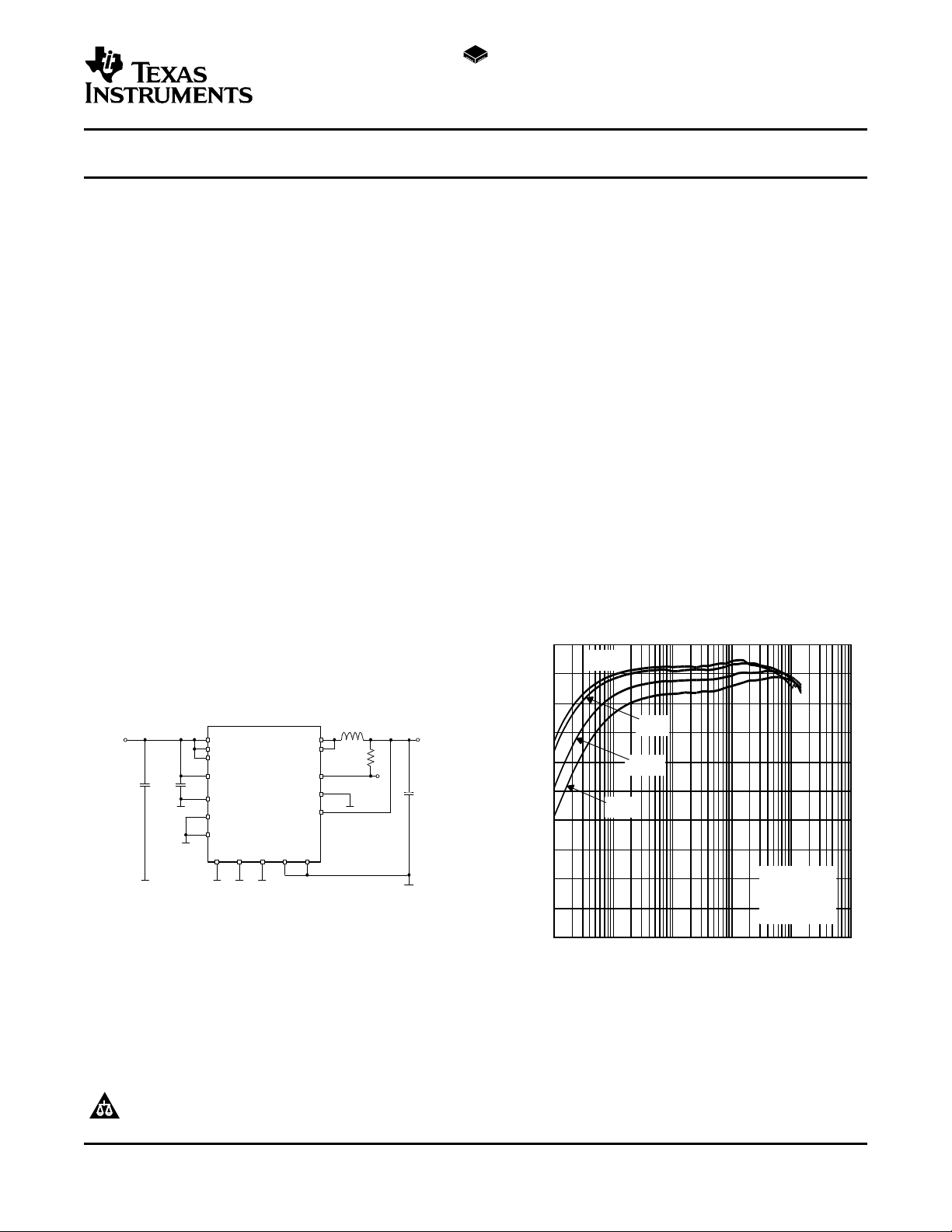
Efficiency vs Output Current
100
0
90
70
40
20
80
50
60
30
10
0.0001 0.001 0.01 0.1 10
1
I - Output Current- A
O
Efficiency - %
5 V
4.2 V
12 V
8.4 V
V = 3.3 V
T
PFM Mode
O
A
= 25 C
o
17-V, 1.5-A, SYNCHRONOUS STEP-DOWN CONVERTER
FEATURES DESCRIPTION
• High-Efficiency Synchronous Step-Down
Converter With up to 95% Efficiency
• 3.1-V to 17-V Operating Input Voltage Range
• Adjustable Output Voltage Range From
1.2 V to 16 V
• Fixed Output Voltage Options Available in
3.3 V and 5 V
• Synchronizable to External Clock Signal up to
1.4 MHz
• Up to 1.5-A Output Current
• High Efficiency Over a Wide Load Current
Range Due to PFM/PWM Operation Mode
• 100% Maximum Duty Cycle for Lowest
Dropout
• 20-µA Quiescent Current (Typical)
• Overtemperature and Overcurrent Protected
• Available in 16-Pin QFN Package
APPLICATIONS
• Point-of-Load Regulation From 12-V Bus
• Organizers, PDAs, and Handheld PCs
• Handheld Scanners
TPS62110
TPS62111
TPS62112
SLVS585 – JULY 2005
The TPS6211x devices are a family of low-noise
synchronous step-down dc-dc converters that are
ideally suited for systems powered from a 2-cell Li-ion
battery or from a 12-V or 15-V rail.
The TPS6211x is a synchronous PWM converter with
integrated – and P-channel power MOSFET switches.
Synchronous rectification is used to increase efficiency and to reduce external component count. To
achieve highest efficiency over a wide load current
range, the converter enters a power-saving,
pulse-frequency modulation (PFM) mode at light load
currents. Operating frequency is typically 1 MHz,
allowing the use of small inductor and capacitor
values. The device can be synchronized to an external clock signal in the range of 0.8 MHz to 1.4 MHz.
For low noise operation, the converter can be
operated in PWM-only mode. In the shutdown mode,
the current consumption is reduced to less than 2 µA.
The TPS6211x is available in the 16-pin (RSA) QFN
package, and operates over a free-air temperature
range of –40 ° C to 85 ° C.
TYPICAL APPLICATION
Please be aware that an important notice concerning availability, standard warranty, and use in critical applications of Texas
Instruments semiconductor products and disclaimers thereto appears at the end of this data sheet.
PowerPAD is a trademark of Texas Instruments.
PRODUCTION DATA information is current as of publication date.
Products conform to specifications per the terms of the Texas
Instruments standard warranty. Production processing does not
necessarily include testing of all parameters.
Copyright © 2005, Texas Instruments Incorporated
www.ti.com
TPS62110
TPS62111
TPS62112
SLVS585 – JULY 2005
This device contains circuits to protect its inputs and outputs against damage due to high static voltages
or electrostatic fields. These circuits have been qualified to protect this device against electrostatic
discharges; HBM according to EIA/JESD22-A114-B, MM according EIA/JESD22-A115-A, and CDM
according EIA/JESD22C101C; however, it is advised that precautions be taken to avoid application of
any voltage higher than maximum-rated voltages to these high-impedance circuits. During storage or
handling the device leads should be shorted together or the device should be placed in conductive foam.
In a circuit, unused inputs should always be connected to an appropriate logic voltage level, preferably
either VCC or ground. Specific guidelines for handling devices of this type are contained in the
publication Guidelines for Handling Electrostatic-Discharge-Sensitive (ESDS) Devices and Assemblies
available from Texas Instruments.
ORDERING INFORMATION
PLASTIC QFN 16 PIN
(RSA) FUNCTIONALITY
TPS62110 Adjustable 1.2 V to 16 V Standard TPS62110
TPS62111 3.3 V Standard TPS62111
TPS62112 5 V Standard TPS62112
(1) The RSA package is available in tape and reel. Add R suffix (TPS62110RSAR) to order quantities of
3000 parts per reel. Add T suffix (TPS62110RSAT) to order quantities of 250 parts per reel.
(1)
OUTPUT VOLTAGE MARKING
LBI/LBO
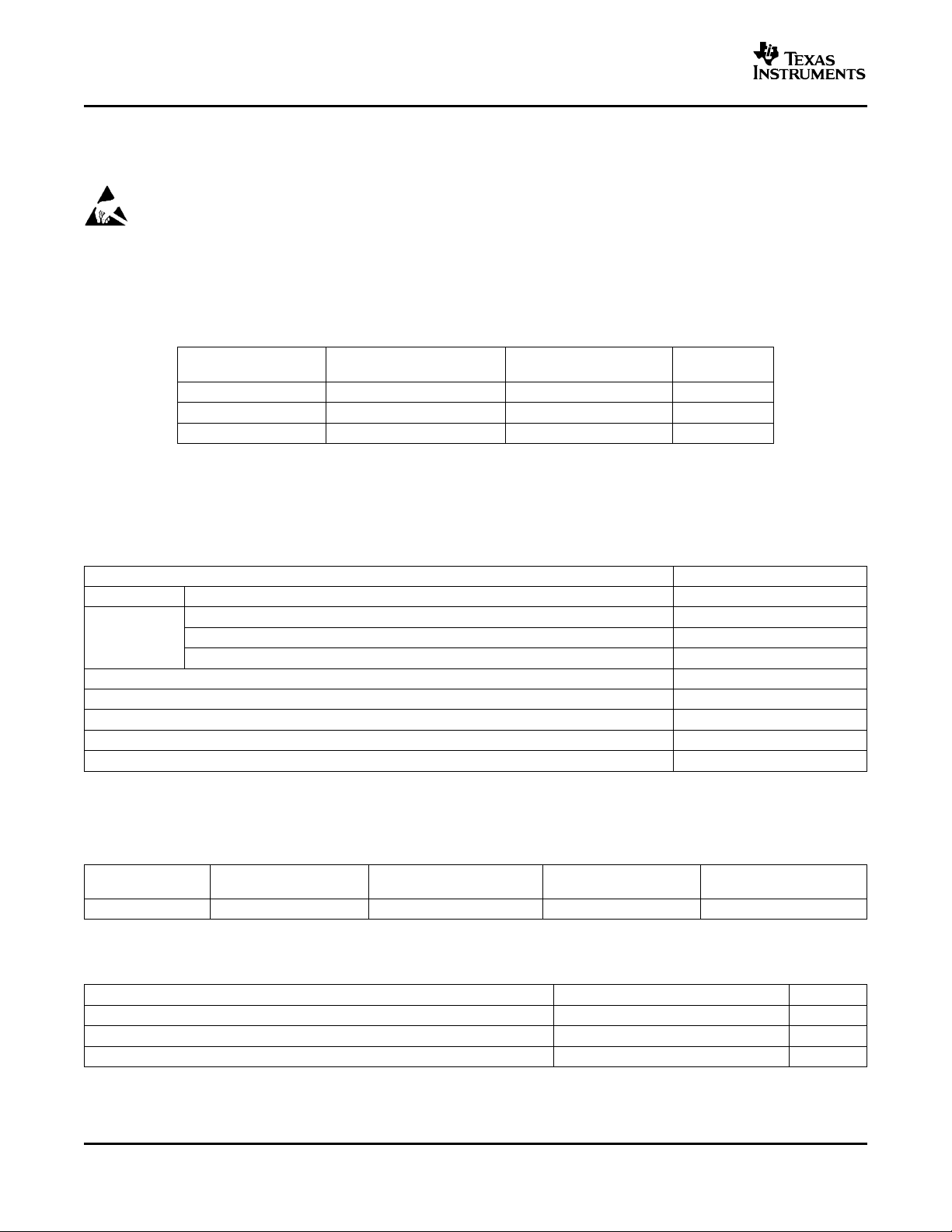
ABSOLUTE MAXIMUM RATINGS
(1)
over operating free-air temperature range (unless otherwise noted)
UNIT
V
CC
V
I
I
O
T
J
T
A
T
stg
(1) Stresses beyond those listed under absolute maximum ratings may cause permanent damage to the device. These are stress ratings
only and functional operation of the device at these or any other conditions beyond those indicated under recommended operating
conditions is not implied. Exposure to absolute-maximum-rated conditions for extended periods may affect device reliability.
DISSIPATION RATINGS
PACKAGE
RSA 2.5 W 25 mW/ ° C 1.375 W 1 W
(1) Based on a thermal resistance of 40 K/W soldered onto a high K board.
Supply voltage at VIN, VINA –0.3 V to 20 V
Voltage at SW –0.3 V to V
Voltage at EN, SYNC, LBO, PG –0.3 V to 20 V
Voltage at LBI, FB –0.3 V to 7 V
Output current at SW 2400 mA
Maximum junction temperature 150 ° C
Operating free-air temperature –40 ° C to 85 ° C
Storage temperature –65 ° C to 150 ° C
Lead temperature 1,6 mm (1/16-inch) from case for 10 seconds 300 ° C
(1)
TA≤ 25 ° C DERATING FACTOR TA= 70 ° C TA= 85 ° C
POWER RATING ABOVE TA= 25 ° C POWER RATING POWER RATING
RECOMMENDED OPERATING CONDITIONS
MIN NOM MAX UNIT
V
T
Supply voltage at VIN , VINA 3.1 17 V
CC
Maximum voltage at power-good, LBO, EN, SYNC 17 V
Operating junction temperature –40 125 ° C
J
I
2
www.ti.com
TPS62110
TPS62111
TPS62112
SLVS585 – JULY 2005
ELECTRICAL CHARACTERISTICS
VI= 12 V, VO= 3.3 V, IO= 600 mA, EN = VI, TA= –40 ° C to 85 ° C (unless otherwise noted)
PARAMETER TEST CONDITIONS MIN TYP MAX UNIT
SUPPLY CURRENT
V
I
(Q)
I
(SD)
ENABLE
V
V
I
IKG
I
(EN)
V
POWER SWITCH
r
DS(ON)
r
DS(ON)
POWER GOOD OUTPUT , LBI, LBO
V
V
I
OL
V
ILBI LBI input leakage current 10 100 nA
V
OSCILLATOR
f
S
f
(SYNC)
V
V
Input voltage range 3.1 17 V
I
IO= 0 mA, SYNC = GND, VI= 7.2 V, 20
Operating quiescent current µA
TA= 25 ° C
IO= 0 mA, SYNC = GND, VI= 17 V
Shutdown current µA
EN high-level input voltage 1.3 V
IH
EN low-level input voltage 0.3 V
IL
EN = GND 1.5 5
EN = GND, TA= 25 ° C, VI= 7.2 V 1.5 3
(1)
(1)
EN trip-point hysteresis 170 mV
EN input leakage current EN = GND or VI, VI= 12 V 0.01 0.2 µA
EN input current 0.6 V ≤ V
Undervoltage lockout threshold Input voltage falling 2.8 3 3.1 V
(UVLO)
≤ 4 V 10 20 µA
(EN)
Undervoltage lockout hysteresis 250 300 mV
VI≥ 5.4 V; IO= 350 mA 165 250
P-channel MOSFET on-resistance VI= 3.5 V; IO= 200 mA 340 m Ω
VI= 3 V; IO= 100 mA 490
P-channel MOSFET leakage
current
V
= 17 V 0.1 1 µA
DS
P-channel MOSFET current limit VI= 7.2 V, VO= 3.3 V 2400 mA
VI≥ 5.4 V; IO= 350 mA 145 200
N-channel MOSFET on-resistance VI= 3.5 V; IO= 200 mA 170 m Ω
VI= 3 V; IO= 100 mA 200
N-channel MOSFET leakage
current
Power good trip voltage VO- V
(PG)
Power good delay time µs
PG, LBO output low voltage V
OL
V
= 17 V 0.1 2 µA
DS
1.6%
VOramping positive 50
VOramping negative 200
= 0.8 × VOnominal, IOL= 1 mA 0.3 V
(FB)
PG, LBO sink current 1 mA
PG, LBO output leakage current V
= VOnominal, V
(FB)
= V
(LBI)
I
0.01 0.25 µA
Minimum supply voltage for valid power 3 V
good, LBI, LBO signal
Low battery input trip voltage Input voltage falling 1.256 V
LBI
Low battery input trip-point
accuracy
Low battery input hysteresis 25 mV
LBI,HYS
Oscillator frequency 900 1000 1100 kHz
Synchronization range CMOS-logic clock signal on SYNC pin 800 1400 kHz
SYNC high-level input voltage 1.5 V
IH
SYNC low-level input voltage 0.3 V
IL
23 26
1.5%
(1) Device is not switching.
3
www.ti.com
TPS62110
TPS62111
TPS62112
SLVS585 – JULY 2005
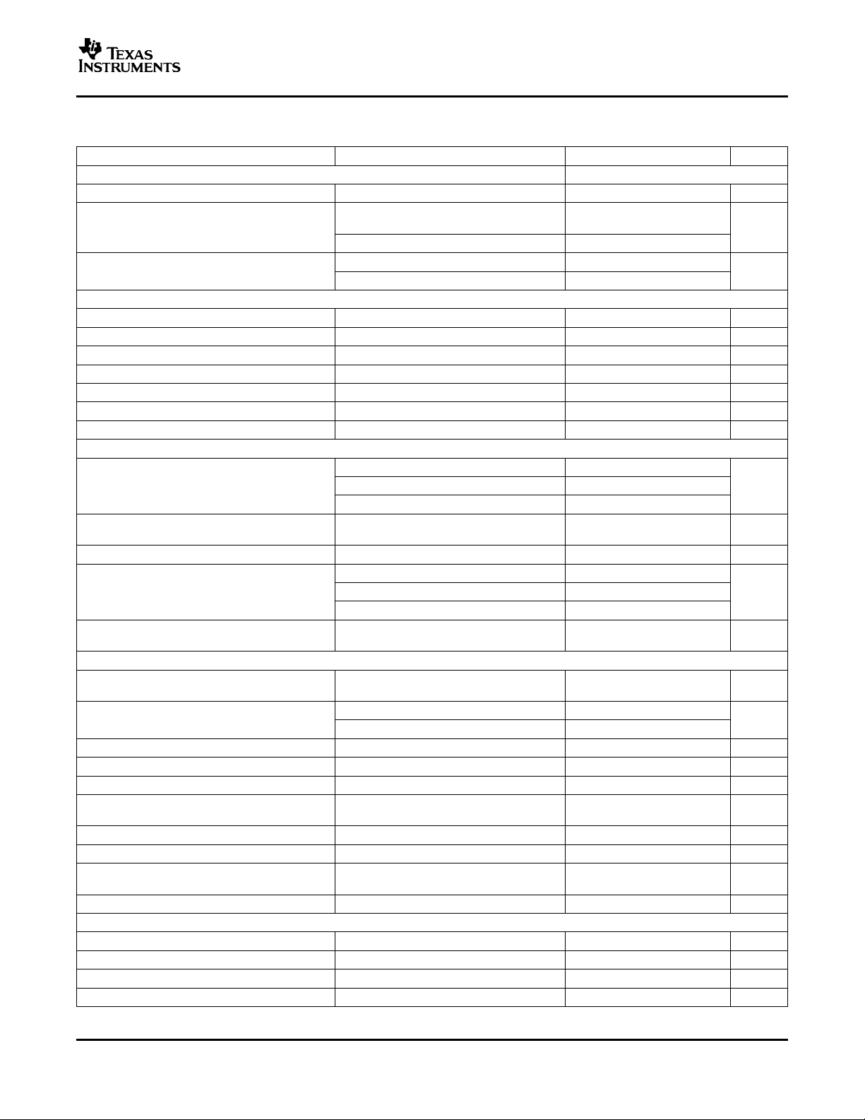
ELECTRICAL CHARACTERISTICS (continued)
VI= 12 V, VO= 3.3 V, IO= 600 mA, EN = VI, TA= –40 ° C to 85 ° C (unless otherwise noted)
PARAMETER TEST CONDITIONS MIN TYP MAX UNIT
I
lkg
OUTPUT
V
V
I
O
η Efficiency 92%
SYNC input leakage current SYNC = GND or VIN 0.01 0.2 µA
SYNC trip-point hysteresis 170 mV
SYNC input current 0.6 V ≤ V
Duty cycle of external clock signal 30% 90%
Adjustable output voltage range TPS62110 1.153 16 V
O
Feedback voltage TPS62110 1.153 V
FB
FB leakage current TPS62110 10 100 nA
Feedback voltage tolerance TPS62110 –2% 2%
Fixed output voltage tolerance
Maximum output current mA
Current into internal voltage divider for
fixed voltage versions
Duty cycle range for main switches at 1 MHz 10% 100%
Minimum tontime for main switch 100 ns
Shutdown temperature 145 ° C
Start-up time IO= 800 mA, VI= 12 V, Vo= 3.3 V 1 ms
(3)
TPS62111 –3% 3%
TPS62112 –3% 3%
VI≥ 3 V (once undervoltage lockout
voltage exceeded)
VI≥ 3.5 V 500
VI≥ 4.3 V 1200
VI≥ 6 V 1500
VI= 7.2 V; VO= 3.3 V; IO= 600 mA
VI= 12 V, Vo= 5 V, Io= 600 mA
≤ 4 V 10 20 µA
(SYNC)
VI= 3.1 V to 17 V;
0 mA < IO< 1500 mA
VI= 3.8 V to 17 V;
0 mA < IO< 1500 mA
VI= 5.5 V to 17 V;
0 mA < IO< 1500 mA
(2)
(2)
(2)
100
5 µA
(2) The maximum output current depends on the input voltage. See the maximum output current for further restrictions on the minimum
input voltage.
(3) The output voltage accuracy includes line and load regulation over the full temperature range TA= -40 ° C to 85 ° C. See the section for
no-load operation in this data sheet.
4

www.ti.com
16 15 14 13
5 6 7 8
1
2
3
4 9
GND
GND
FB
AGND
PGND
Exposed
Thermal
Pad
VIN
VIN
EN
PGND
SW
LBI
VINA
SW
PG
SYNC
LBO
12
11
10
TPS62110
TPS62111
TPS62112
SLVS585 – JULY 2005
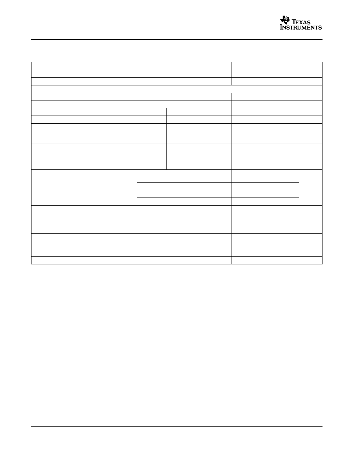
DEVICE INFORMATION
PIN ASSIGNMENT TOP VIEW
TERMINAL FUNCTIONS
TERMINAL
NAME NO.
EN 4 I
FB 10 I
LBO 6 O Open-drain, low-battery output. This pin is pulled low if LBI is below its threshold.
GND 11, 12 I Ground
LBI 7 I Low-battery input
SW 14, 15 O
PG 13 O between PG and VOUT. The output goes active high when the output voltage is greater than 98.4% of
PGND 1, 16 I Power ground. Connect all power grounds to this pin.
AGND 9 I Analog ground, connect to GND and PGND
SYNC 5 I Input for synchronization to external clock signal. Synchronizes the converter switching frequency to an
VIN 2, 3 I Supply voltage input (power stage)
VINA 8 I Supply voltage input (support circuits)
PowerPAD™ Connect to AGND
I/O DESCRIPTION
Enable. A logic high enables the converter; logic low forces the device into shutdown mode reducing the
supply current to less than 2 µA.
Feedback pin for the fixed output voltage option. For the adjustable version, an external resistive divider
is connected to this pin. The internal voltage divider is disabled for the adjustable version.
Connect the inductor to this pin. This pin is the switch pin and connected to the drain of the internal
power MOSFETS.
Power good comparator output. This is an open-drain output. A pullup resistor should be connected
the nominal value.
external clock signal with CMOS level:
SYNC = HIGH: Low-noise mode enabled, fixed frequency PWM operation is forced
SYNC = LOW (GND): Power save mode enabled, PFM/PWM Mode enabled
5
www.ti.com
_
+
_
+
_
+
_
+
_
+
REF
REF
Load Comparator
I
AVG
Comparator
Current Limit Comparator
P-Channel
Power MOSFET
Driver
Shoot-Through
Logic
Control
Logic
Soft Start
1-MHz
Oscillator
Comparator
S
R
N-Channel
Power MOSFET
Comparator High
Comparator Low
Comparator High 2
V
(COMP)
Sawtooth
Generator
V
I
Undervoltage
Lockout
Bias Supply
_
+
Comparator High
Comparator Low
Compensation
V = 1.153 V
REF
R2
(See Note A)
R1
V
I
EN
SW
FB PGND
Gm
Thermal
Shutdown
Vina
_
+
_
+
SKIP Comparator
_
+
_
+
PG
LBO
LBI
GND
1.256 V
TPS62110
TPS62111
TPS62112
SLVS585 – JULY 2005
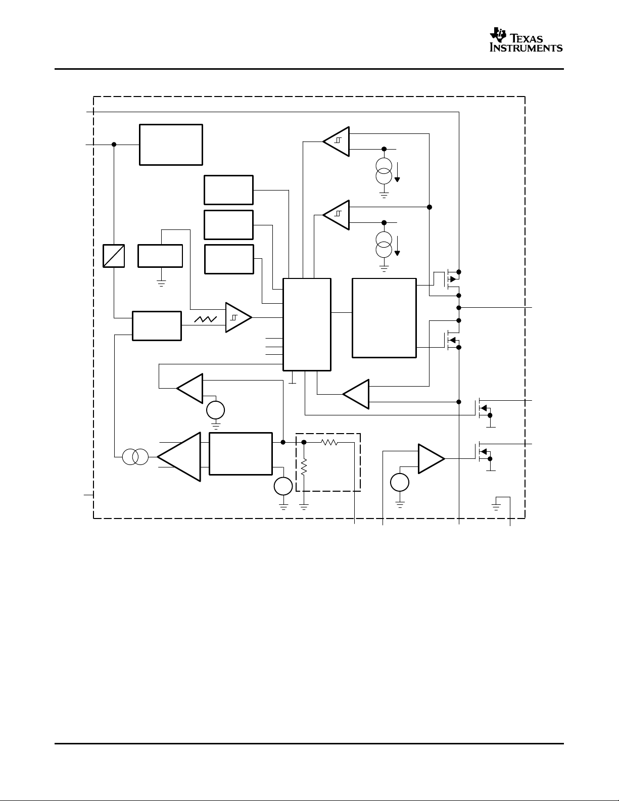
FUNCTIONAL BLOCK DIAGRAM
A. For the adjustable version (TPS62110), the internal feedback divider is disabled and the FB pin is directly connected
to the internal GM amplifier.
6
www.ti.com
100
0
90
70
40
20
80
50
60
30
10
0.0001 0.001 0.01 0.1 10
1
I - Output Current- A
O
Efficiency - %
15 V
12 V
8.4 V
V = 5 V
T
PWM Mode
O
A
= 25 C
o
100
0
90
70
40
20
80
50
60
30
10
0.0001 0.001 0.01 0.1 10
1
I - Output Current- A
O
Efficiency - %
15 V
12 V
8.4 V
V = 5 V
T
PFM Mode
O
A
= 25 C
o
TPS62110
TPS62111
TPS62112
SLVS585 – JULY 2005
TYPICAL CHARACTERISTICS
Table of Graphs
FIGURE
Efficiency vs Output current (5 V) 1, 2
Efficiency vs Output current (3.3 V) 3, 4, 5
Maximum output current vs Input voltage 6
Efficiency vs Output current (1.8 V) 7, 8
Efficiency vs Output current (1.5 V) 9, 10
Line transient response 11
Load transient response 12
Output ripple 13
Start-up timing 14
Switching frequency vs Input voltage 15
Quiescent current vs Input voltage 16
Graphs with V
= 1.8 V were taken using the circuit according to Figure 20 .
O
TPS62112 TPS62112
EFFICIENCY EFFICIENCY
OUTPUT CURRENT OUTPUT CURRENT
vs vs
Figure 1. Figure 2.
7

www.ti.com
100
0
90
70
40
20
80
50
60
30
10
0.0001 0.001 0.01 0.1 10
1
I - Output Current- A
O
Efficiency - %
5 V
4.2 V
12 V
8.4 V
V = 3.3 V
T
PWM Mode
O
A
= 25 C
o
100
0
90
70
40
20
80
50
60
30
10
0.0001 0.001 0.01 0.1 10
1
I - Output Current- A
O
Efficiency - %
5 V
4.2 V
12 V
8.4 V
V = 3.3 V
T
PFM Mode
O
A
= 25 C
o
2000
1600
1100
1800
1400
900
700
400
100
1900
1500
1000
1700
1200
1300
800
500
200
600
300
0
3.2 3.6 5.245.6 6
4.4
4.8
V - Input Voltage- V
I
I - Output Current - mA
O
100
0
90
70
40
20
80
50
60
30
10
0.0001 0.001 0.01 0.1 10
1
I - Output Current- A
O
Efficiency - %
5 V
12 V
8.4 V
V = 3.3 V
SYNC = 1.4 MHz
T
PFM Mode
O
A
= 25 C
o
TPS62110
TPS62111
TPS62112
SLVS585 – JULY 2005
TPS62111 TPS62111
EFFICIENCY EFFICIENCY
vs vs
OUTPUT CURRENT OUTPUT CURRENT
Figure 3. Figure 4.
TPS62111 TPS62111
EFFICIENCY MAXIMUM OUTPUT CURRENT
OUTPUT CURRENT INPUT VOLTAGE
Figure 5. Figure 6.
8
vs vs

www.ti.com
100
0
90
70
40
20
80
50
60
30
10
0.0001 0.001 0.01 0.1 10
1
I - Output Current- A
O
Efficiency - %
5 V
4.2 V
12 V
8.4 V
V = 1.8 V
T
PFM Mode
O
A
= 25 C
o
100
0
90
70
40
20
80
50
60
30
10
0.0001 0.001 0.01 0.1 10
1
I - Output Current- A
O
Efficiency - %
5 V
4.2 V
12 V
8.4 V
V = 1.8 V
T
PWM Mode
O
A
= 25 C
o
100
0
90
70
40
20
80
50
60
30
10
0.0001 0.001 0.01 0.1 10
1
I - Output Current- A
O
Efficiency - %
5 V
4.2 V
12 V
8.4 V
V = 1.5 V
T
PFM Mode
O
A
= 25 C
o
100
0
90
70
40
20
80
50
60
30
10
0.0001 0.001 0.01 0.1 10
1
I - Output Current- A
O
Efficiency - %
5 V
4.2 V
12 V
8.4 V
V = 1.5 V
T
PWM Mode
O
A
= 25 C
o
TPS62110 TPS62110
EFFICIENCY EFFICIENCY
vs vs
OUTPUT CURRENT OUTPUT CURRENT
TPS62110
TPS62111
TPS62112
SLVS585 – JULY 2005
Figure 7. Figure 8.
TPS62110 TPS62110
EFFICIENCY EFFICIENCY
OUTPUT CURRENT OUTPUT CURRENT
Figure 9. Figure 10.
vs vs
9

www.ti.com
t − Time = 2 ms/div
VI = 7.2 V to 12 V
VO = 3.3 V
I
LOAD
= 800 mA
TA = 25°C
C2 = 50 mV/div
C1 = 5 V/div
t − Time = 20 µs/div
VI = 8.4 V
VO = 3.3 V
I
LOAD
= 150 mA to 1350 mA
TA = 25°C
VO = 50 mV/div
IO = 500 mA/div
t − Time = 5 µs/div
CH1 = 20 mV/div
VI = 8.4 V, VO = 3.3 V
CH2 =
5 V/div
CH4 = 200 mA/div
I
LOAD
= 100 mA, TA = 25°C
t − Time = 200 µs/div
CH1 = 10 V/div
VI = 12 V, VO = 3.3 V
CH4 = 500 mA/div
I
LOAD
= 800 mA, TA = 25°C
CH3 = 5 V/div
CH2 = 1 V/div
TPS62110
TPS62111
TPS62112
SLVS585 – JULY 2005
TPS62111 TPS62111
LINE TRANSIENT LOAD TRANSIENT
Figure 11. Figure 12.
TPS62111 TPS62111
OUTPUT RIPPLE START-UP TIMING
Figure 13. Figure 14.
10

www.ti.com
1000
970
930
940
900
980
950
910
990
960
920
3
7
5
948
6 10
1412
16
11
1513
17
V - Input Voltage - V
I
Switching Frequency - kHz
25 C
o
-40 C
o
85 C
o
V = 12 V
I
O
O
= 100 mA
0
10
30
20
40
5
15
35
25
45
50
3
7
5
948
6 10
1412
16
11
1513
17
V - Input Voltage - V
I
Quiescent Current - Am
25 C
o
-40 C
o
85 C
o
SYNC
GND PGND
SW
R1
R2
V
O
TDK 6.8 H
SLF7032T-6R8M1R6
m
C 22 F / 16 V
TDK
O
m
C3225X7R1C226M
VIN
LBI
C 10 F / 25 V
TDK
I
m
C3225X5R1E106K
1 Fm
261 kW
Vbat
VIN
EN
VINA
PGNDGND PwPD
open
VIN or
GND
AGND
TPS62110
SW
LBO
PG
1 MW 1 MW
FB
C
ff
TPS62110
TPS62111
TPS62112
SLVS585 – JULY 2005
SWITCHING FREQUENCY QUIESCENT CURRENT
vs vs
INPUT VOLTAGE INPUT VOLTAGE
Figure 15. Figure 16.
The graphs were generated using the EVM with the setup according to Figure 17 unless otherwise noted. The
output voltage divider was adjusted according to Table 4 . Graphs for an output voltage of 5 V and 3.3 V were
generated using TPS62111 and TPS62112 with R1 = 0 Ω and R2 = open.
Figure 17. Test Setup
11

www.ti.com
TPS62110
TPS62111
TPS62112
SLVS585 – JULY 2005
DETAILED DESCRIPTION
OPERATION
The TPS6211x is a synchronous step-down converter that operates with a 1-MHz fixed frequency pulse width
modulation (PWM) at moderate-to-heavy load currents and enters the power save mode at light load current.
During PWM operation, the converter uses a unique fast response voltage mode control scheme with input
voltage feedforward. Good line and load regulation is achieved with the use of small input and output ceramic
capacitors. At the beginning of each clock cycle initiated by the clock signal (S), the P-channel MOSFET switch
is turned on, and the inductor current ramps up until the comparator trips and the control logic turns the switch
off. The switch is turned off by the current limit comparator if the current limit of the P-channel switch is
exceeded. After the dead time prevents current shoot through, the N-channel MOSFET rectifier is turned on, and
the inductor current ramps down. The next cycle is initiated by the clock signal turning off the N-channel rectifier,
and turning on the P-channel switch.
The error amplifier as well as the input voltage determines the rise time of the sawtooth generator. Therefore,
any change in input voltage or output voltage directly controls the duty cycle of the converter giving a very good
line and load transient regulation.
CONSTANT FREQUENCY MODE OPERATION (SYNC = HIGH)
In constant frequency mode, the output voltage is regulated by varying the duty cycle of the PWM signal in the
range of 100% to 10%. Connecting the SYNC pin to a voltage greater than 1.5 V forces the converter to operate
permanently in the PWM mode even at light or no-load currents. The advantage is that the converter operates
with a fixed switching frequency that allows simple filtering of the switching frequency for noise-sensitive
applications. In this mode, the efficiency is lower compared to the power save mode during light loads. The
N-MOSFET of the devices stay on even when the current into the output drops to zero. This prevents the device
from going into discontinuous mode, and the device transfers unused energy back to the input. Therefore, there
is no ringing at the output, which usually occurs in discontinuous mode. The duty cycle range in constant
frequency mode is 100% to 10%.
It is possible to switch from forced PWM mode to the power save mode during operation by pulling the SYNC pin
LOW. The flexible configuration of the SYNC pin during operation of the device allows efficient power
management by adjusting the operation of the TPS6211x to the specific system requirements.
POWER SAVE MODE OPERATION (SYNC = LOW)
As the load current decreases, the converter enters the power save mode operation. During power save mode,
the converter operates with reduced switching frequency in pulse frequency modulation (PFM), and with a
minimum quiescent current to maintain high efficiency. Whenever the average output current goes below the skip
threshold, the converter enters the power save mode. The average current depends on the input voltage. It is
about 200 mA at low input voltages and up to 400 mA with maximum input voltage. The average output current
must be below the threshold for at least 32 clock cycles to enter the power save mode. During the power save
mode, the output voltage is monitored with a comparator and the output voltage is regulated in to a typical value
between the nominal output voltage and 0.8% above the nominal output voltage. When the output voltage falls
below the nominal output voltage, the P-channel switch turns on. The P-channel switch is turned off as the peak
switch current is reached. The N-channel rectifier is turned on, and the inductor current ramps down. As the
inductor current approaches zero, the N-channel rectifier is turned off and the switch is turned on starting the
next pulse. When the output voltage can not be reached with a single pulse, the device continues to switch with
its normal operating frequency until the comparator detects the output voltage to be 0.8% above the nominal
output voltage. This control method reduces the quiescent current to 20 µA (typical), and reduces the switching
frequency to a minimum that achieves the highest converter efficiency.
12

www.ti.com
V (nominal)
O
0.8%
1.6%
-1.6%
t
W
»
2 5
I
V
S K I P
I
( )
)(
max
)(
maxmaxmin
L
R
onDS
r
O
I
O
V
I
V +×+=
DETAILED DESCRIPTION (continued)
Figure 18. Power Save Mode Output Voltage Thresholds
The typical PFM (SKIP) current threshold for the TPS6211x is given by:
TPS62110
TPS62111
TPS62112
SLVS585 – JULY 2005
Equation 1 is valid for input voltages up to 7 V. For higher voltages, the skip current threshold is not increased
further. The converter enters the fixed frequency PWM mode as soon as the output voltage falls below V
(nominal).
- 1.6%
O
SOFT START
The TPS6211x has an internal soft-start circuit that limits the inrush current during start-up. This prevents
possible voltage drops of the input voltage when a battery or a high-impedance power source is connected to the
input of the TPS6211x.
The soft start is implemented as a digital circuit increasing the switch current in steps of 300 mA, 600 mA, 1200
mA. The typical switch current limit is 2.4 A. Therefore, the start-up time depends on the output capacitor and
load current. Typical start-up time with a 22-µF output capacitor and 800-mA load current is 1 ms.
100% DUTY CYCLE LOW DROPOUT OPERATION
The TPS6211x offers the lowest possible input to output voltage difference while still maintaining operation with
the use of the 100% duty cycle mode. In this mode, the P-channel switch is constantly turned on. This is
particularly useful in battery-powered applications to achieve the longest operation time, taking full advantage of
the whole battery voltage range. The minimum input voltage to maintain regulation depends on the load current
and output voltage, and is calculated as:
with:
IOmax = maximum output current plus inductor ripple current
r
max = maximum P-channel switch r
DS(on)
R
= dc resistance of the inductor
(L)
VOmax = nominal output voltage plus maximum output voltage tolerance
DS(on)
(1)
(2)
13

www.ti.com
TPS62110
TPS62111
TPS62112
SLVS585 – JULY 2005
DETAILED DESCRIPTION (continued)
ENABLE
Logic low on EN forces the TPS6211x into shutdown. In shutdown, the power switch, drivers, voltage reference,
oscillator, and all other functions are turned off. The supply current is reduced to less than 2 µA in the shutdown
mode. When the device is in thermal shutdown, the bandgap is forced to be switched on even if the device is set
into shutdown by pulling EN to GND.
If an output voltage is present when the device is disabled, which could be due to an external voltage source or a super capacitor, the reverse leakage current is specified under electrical characteristics. Pulling the enable pin high starts up the TPS6211x with the soft start. If the EN pin is connected to any voltage other than VIor GND, an increased leakage current of typically 10 µA and up to 20 µA can occur.
UNDERVOLTAGE LOCKOUT
The undervoltage lockout circuit prevents the device from misoperation at low-input voltages. It prevents the
converter from turning on the switch or rectifier MOSFET under undefined conditions. The minimum input voltage
to start up the TPS6211x is 3.4 V (worst case). The device shuts down at 2.8 V minimum.
SYNCHRONIZATION
If no clock signal is applied, the converter operates with a typical switching frequency of 1 MHz. It is possible to
synchronize the converter to an external clock within a frequency range from 0.8 MHz to 1.4 MHz. The device
automatically detects the rising edge of the first clock and synchronizes immediately to the external clock. If the
clock signal is stopped, the converter automatically switches back to the internal clock and continues operation.
The switch over is initiated if no rising edge on the SYNC pin is detected for a duration of four clock cycles.
Therefore, the maximum delay time can be 6.25 µs if the internal clock has its minimum frequency of 800 kHz
If the device is synchronized to an external clock, the power save mode is disabled, and the devices stay in
forced PWM mode.
Connecting the SYNC pin to the GND pin enables the power save mode. The converter operates in the PWM
mode at moderate-to-heavy loads, and in the PFM mode during light loads which maintains high efficiency over a
wide load current range.
POWER GOOD COMPARATOR
The power good (PG) comparator has an open-drain output capable of sinking 1 mA (typical). The PG is only
active when the device is enabled (EN=high). When the device is disabled (EN=low), the PG pin is pulled to
GND.
The PG output is only valid after a 250-µs delay when the device is enabled, and the supply voltage is greater
than the undervoltage lockout V
The PG pin becomes active high when the output voltage exceeds 98.4% (typical) of its nominal value. Leave
the PG pin unconnected when not used.
. PG is low during the first 250 µs after shutdown and in shutdown.
(UVLO)
LOW-BATTERY DETECTOR
The low-battery output (LBO) is an open-drain type which goes low when the voltage at the low-battery input
(LBI) falls below the trip point of 1.256 V ± 1.5%. The voltage at which the low-battery warning is issued can be
adjusted with a resistive divider as shown in Figure 19 . The sum of resistors (R1 + R2) as well as the sum of (R5
+ R6) is recommended to be in the 100-k Ω to 1-M Ω range for high efficiency at low output current. An external
pullup resistor can be connected to OUT, or any other voltage rail in the voltage range of 0 V to 16 V. During
start-up, the LBO output signal is invalid for the first 500 µs. LBO is high impedance when the device is disabled.
If the low-battery comparator function is not used, connect LBI to ground. The low-battery detector is disabled
when the device is disabled.
The logic level of the LBO pin is not defined for the first 500 µs after EN is pulled high.
When the LBI is used to supervise the battery voltage and shut down the TPS62111 at low-input voltages, the
battery voltage rises when the current drops to zero. The implemented hysteresis on the LBI pin may not be
sufficient for all types of batteries. Figure 19 shows how an additional external hysteresis can be implemented.
14

www.ti.com
SYNC
GND PGND
SW
R1
560 k
R2
300 k
V
O
= 3.3 V
6.8 Hm
C = 22 F
6.3 V
O
m
VIN
LBI
C = 10 F
25 V
I
m
1 Fm
2
3
4
8
9
7
5
11 12
16
10
6
13
14
15
1
V = 4.3 V to 17 V
I
VIN
EN
VINA
PGNDGND PwPD
R5
R6
AGND
TPS62110
SW
LBO
PG
R3
R7
R4
FB
C
ff
10 pF
TPS62110
TPS62111
TPS62112
SLVS585 – JULY 2005
DETAILED DESCRIPTION (continued)
Figure 19. LBI With Increased Hysteresis
NO LOAD OPERATION
When the converter operates in the forced PWM mode and there is no load connected to the output, the
converter regulates the output voltage by allowing the inductor current to reverse for a short time.
THEORY OR OPERATION / DESIGN PROCEDURE
Table 1. List of Inductors
MANUFACTURER
Coilcraft MSS6132-682 6.8 µH 65 mR (max) 1.5 A
Epcos B82462G4682M 6.8 µH 50 mR (max) 1.5 A
Sumida CDRH5D28-6R2 6.2 µH 33 mR (typ) 1.8 A
TDK
Wurth 7447779006 6.8 µH 33 mR (typ) 3.3 A
(1) The manufacturer's part numbers are used for test purposes only.
(1)
TYPE INDUCTANCE DC RESISTANCE SATURATION CURRENT
SLF6028T-6R8M1R5 6.8 µH 35 mR (typ) 1.5 A
SLF7032T-6R8M1R6 6.8 µH 41 mR (typ) 1.6 A
7447789006 6.8 µH 44 mR (typ) 2.75 A
744053006 6.2 µH 45 mR (typ) 1.8 A
Inductor Selection
The control loop of the TPS6211x family requires a certain value for the output inductor and the output capacitor
for stable operation. As long as the nominal value of L × C ≥ 6.2 µH × 22 µF, the control loop has enough phase
margin and the device is stable. Reducing the inductor value without increasing the output capacitor (or vice
versa) may cause stability problems. There are applications where it may be useful to increase the value of the
output capacitor, e.g., for a low transient output voltage change. From a stability point of view, the inductor value
could be decreased to keep the L × C product constant. However, there are drawbacks if the inductor value is
decreased. A low inductor value causes a high inductor ripple current and therefore reduces the maximum dc
output current. Table 2 gives the advantages and disadvantages when designing the inductor and output
capacitor.
15

www.ti.com
fL
I
V
O
V
O
V
L
I
´
-
´=D
1
2
m a xm a x
L
I
O
I
L
I
D
+=
TPS62110
TPS62111
TPS62112
SLVS585 – JULY 2005
Table 2. Advantages and Disadvantages When Designing the Inductor and Output Capacitor
INFLUENCE ON STABILITY ADVANTAGE DISADVANTAGE
Less output voltage ripple
Increase Cout (>22 µF) Uncritical None
Decrease Cout (<22 µF) Increase inductor value >6.8 µH None undershoot during load transi-
Increase L (>6.8 µH)
Decrease L (<6.8 µH)
Critical High output voltage overshoot /
also ent
Uncritical Less inductor current ripple More energy stored in the in-
Critical High inductor current ripple esIncrease output capacitor value >
22 µF also
Less output voltage overshoot / undershoot during load transient
Higher output voltage ripple
Less gain and phase margin
ductor → higher voltage overshoot during load transient
Higher dc output current possible if Smaller current rise → higher
operated close to the current limit voltage undershoot during load
Small voltage overshoot / undershoot during load transient
transient → do not decrease the
value of Cout due to these effects
pecially at high input voltage
and low output voltage
As it is shown in Table 2 , the inductor value can be increased to higher values. For good performance, the
peak-to-peak inductor current ripple should be less than 30% of the maximum dc output current. Especially at
input voltages above 12 V, it makes sense to increase the inductor value in order to keep the inductor current
ripple low. In such applications, the inductor value can be increased to 10 µH or 22 µH. Values above 22 µH
should be avoided in order to keep the voltage overshoot during load transient in an acceptable range.
After choosing the inductor value, two additional inductor parameters should be considered:
1. current rating of the inductor
2. dc resistance
The dc resistance of the inductance directly influences the efficiency of the converter. Therefore, an inductor with
lowest dc resistance should be selected for highest efficiency. In order to avoid saturation of the inductor, the
inductor should be rated at least for the maximum output current plus the inductor ripple current which is
calculated as:
Where:
f = Switching frequency (1000 kHz typical)
L = Inductor value
∆ IL= Peak-to-peak inductor ripple current
IL(max) = Maximum inductor current
The highest inductor current occurs at maximum VI. A more conservative approach is to select the inductor
current rating just for the maximum switch current of the TPS6211x which is 2.4 A (typically). See Table 1 for
recommended inductors.
(3)
OUTPUT CAPACITOR SELECTION
A 22- µ F (typical) output capacitor is needed with a 6.8- µ H inductor. For an output voltage greater than 5 V, a
33- µ F (minimum) output capacitor is required for stability. For best performance, a low ESR ceramic output
capacitor is needed.
Just for completeness, the RMS ripple current is calculated as:
16

www.ti.com
32
1
1
)(
´
´
´
-
´=
fL
I
V
O
V
O
V
O
C
R M S
I
÷
÷
ø
ö
ç
ç
è
æ
+
´´
´
´
-
´=D
E S R
R
f
O
CfL
I
V
O
V
O
V
O
V
8
1
1
÷
÷
ø
ö
ç
ç
è
æ
-´´=
I
V
O
V
I
V
O
V
O
I
R M S
I 1m a x
TPS62110
TPS62111
TPS62112
SLVS585 – JULY 2005
The overall output ripple voltage is the sum of the voltage spike caused by the output capacitor ESR plus the
voltage ripple caused by charge and discharging the output capacitor:
Where the highest output voltage ripple occurs at the highest input voltage VI.
INPUT CAPACITOR SELECTION
The nature of the buck converter is a pulsating input current; therefore, a low ESR input capacitor is required for
best input voltage filtering, and minimizing the interference with other circuits caused by high input voltage
spikes. The input capacitor should have a minimum value of 10 µF and can be increased without any limit for
better input voltage filtering. The input capacitor should be rated for the maximum input ripple current calculated
as:
(4)
(5)
The worst-case RMS ripple current occurs at D = 0.5 and is calculated as: I
= IO/2. Ceramic capacitors show
RMS
a good performance because of their low ESR value, and they are less sensitive against voltage transients
compared to tantalum capacitors. Place the input capacitor as close as possible to the input pin of the IC for best
performance
FEEDFORWARD CAPACITOR SELECTION
The feedforward capacitor (C
Typically, a value of 4.7 pF to 22 pF is needed for an output voltage divider with a equivalent resistance (R1 in
parallel with R2) in the 150-k Ω range. The value can be chosen based on best transient performance and lowest
output voltage ripple in PFM mode.
) is needed to compensate for parasitic capacitance from the feedback pin to GND.
ff
RECOMMENDED CAPACITORS
It is recommended that only X5R or X7R ceramic capacitors be used as input/output capacitors. Ceramic
capacitors show a dc-bias effect. This effect reduces the effective capacitance when a dc-bias voltage is applied
across a ceramic capacitor, as on the output and input capacitor of a dc/dc converter. The effect may lead to a
significant capacitance drop especially for high input/output voltages and small capacitor packages. See the
manufacturer's data sheet about the performance with a dc bias voltage applied. It may be necessary to choose
a higher voltage rating or nominal capacitance value in order to get the required value at the operating point. The
capacitors listed in Table 3 have been tested with the TPS62110 with good performance.
Table 3. List of Capacitors
MANUFACTURER PART NUMBER SIZE VOLTAGE CAPACITANCE TYPE
Taiyo Yuden Ceramic
TDK C3225X7R1C226M 16 V 22 µF Ceramic
TMK316BJ106KL 1206 25 V 10 µF
EMK325BJ226KM 1210 16 V 22 µF
C3225X5R1E106M 25 V 10 µF
C3216X5R1E106MT 1206 25 V 10 µF
1210
(6)
17

www.ti.com
SYNC
GND PGND
SW
R1
220 kW
R2
390 kW
V
O
= 1.8 V
6.8 Hm
C = 2 x 22 F
6.3 V
O
m
VIN
LBI
C = 10 F
25 V
I
m
1 Fm
2
3
4
8
9
7
5
11 12
16
10
6
13
14
15
1
V = 3.5 V to 17 V
I
VIN
EN
VINA
PGNDGND PwPD
R5
R6
AGND
TPS62110
SW
LBO
PG
R3
1 MW
R4
1 MW
FB
C
ff
10 pF
221R
RR
F B
V
O
V
+
´=
221 R
F B
V
O
V
RR -
÷
÷
ø
ö
ç
ç
è
æ
´=
SYNC
GND PGND
SW
V
O
= 5 V
6.8 Hm
C = 22 F
10 V
O
m
VIN
LBI
C = 10 F
25 V
I
m
1 Fm
2
3
4
8
9
7
5
11 12
16
10
6
13
14
15
1
V = 5.5 V to 17 V
I
VIN
EN
VINA
PGNDGND PwPD
AGND
TPS62112
SW
LBO
PG
1 MW
FB
TPS62110
TPS62111
TPS62112
SLVS585 – JULY 2005
APPLICATION INFORMATION
A. For an output voltage lower than 2.5 V, an output capacitor of 33 µ F or greater is recommended to improve load
transient.
Figure 20. Standard Connection for Adjustable Version
V
FB
= 1.153 V
Table 4. Recommended Resistors
OUTPUT VOLTAGE R1 R2 NOMINAL VOLTAGE TYPICAL C
9 V 680 k Ω 100 k Ω 8.993 V 22 pF
5 V 510 k Ω 150 k Ω 5.073 V 10 pF
3.3 V 560 k Ω 300 k Ω 3.305 V 10 pF
2.5 V 390 k Ω 330 k Ω 2.515 V 10 pF
1.8 V 220 k Ω 390 k Ω 1.803 V 10 pF
1.5 V 100 k Ω 330 k Ω 1.502 V 10 pF
(7)
ff
18
Figure 21. Standard Connection for Fixed Voltage Version

www.ti.com
SYNC
GND PGND
SW
R1
680 kW
R2
100 kW
V
O
= 9 V
6.8 Hm
C = 33 F
16 V
O
m
VIN
LBI
C = 10 F
25 V
I
m
1 Fm
2
3
4
8
9
7
5
11 12
16
10
6
13
14
15
1
V = 9.3 V to 17 V
I
VIN
EN
VINA
PGNDGND PwPD
AGND
TPS62110
SW
LBO
PG
1 MW
FB
C
ff
22 pF
A. For an output voltage greater than 5 V, an output capacitor of 33 µ F minimum is required for stability.
Figure 22. Application With 9-V Output
TPS62110
TPS62111
TPS62112
SLVS585 – JULY 2005
19


PACKAGE OPTION ADDENDUM
www.ti.com
27-Sep-2005
PACKAGING INFORMATION
Orderable Device Status
(1)
Package
Type
Package
Drawing
Pins Package
Qty
Eco Plan
TPS62110RSAR ACTIVE QFN RSA 16 3000 Green (RoHS &
no Sb/Br)
TPS62110RSARG4 ACTIVE QFN RSA 16 3000 Green (RoHS &
no Sb/Br)
TPS62110RSAT ACTIVE QFN RSA 16 250 Green (RoHS &
no Sb/Br)
TPS62110RSATG4 ACTIVE QFN RSA 16 250 Green (RoHS &
no Sb/Br)
TPS62111RSAR ACTIVE QFN RSA 16 3000 Green (RoHS &
no Sb/Br)
TPS62111RSARG4 ACTIVE QFN RSA 16 3000 Green (RoHS &
no Sb/Br)
TPS62111RSAT ACTIVE QFN RSA 16 250 Green (RoHS &
no Sb/Br)
TPS62111RSATG4 ACTIVE QFN RSA 16 250 Green (RoHS &
no Sb/Br)
TPS62112RSAR ACTIVE QFN RSA 16 3000 Green (RoHS &
no Sb/Br)
TPS62112RSARG4 ACTIVE QFN RSA 16 3000 Green (RoHS &
no Sb/Br)
TPS62112RSAT ACTIVE QFN RSA 16 250 Green (RoHS &
no Sb/Br)
TPS62112RSATG4 ACTIVE QFN RSA 16 250 Green (RoHS &
no Sb/Br)
(1)
The marketing status values are defined as follows:
ACTIVE: Product device recommended for new designs.
LIFEBUY: TI has announced that the device will bediscontinued,and a lifetime-buy period is in effect.
NRND: Not recommended for new designs. Device is in production to support existing customers, but TI does not recommend using this part in
a new design.
PREVIEW: Device has been announced but is not in production. Samples may or may not be available.
OBSOLETE: TI has discontinued the production of the device.
(2)
Lead/Ball Finish MSL Peak Temp
CU NIPDAU Level-2-260C-1 YEAR
CU NIPDAU Level-2-260C-1 YEAR
CU NIPDAU Level-2-260C-1 YEAR
CU NIPDAU Level-2-260C-1 YEAR
CU NIPDAU Level-2-260C-1 YEAR
CU NIPDAU Level-2-260C-1 YEAR
CU NIPDAU Level-2-260C-1 YEAR
CU NIPDAU Level-2-260C-1 YEAR
CU NIPDAU Level-2-260C-1 YEAR
CU NIPDAU Level-2-260C-1 YEAR
CU NIPDAU Level-2-260C-1 YEAR
CU NIPDAU Level-2-260C-1 YEAR
(3)
(2)
Eco Plan - The planned eco-friendly classification: Pb-Free (RoHS) or Green (RoHS & no Sb/Br) - please check
http://www.ti.com/productcontent for the latest availability information and additional product content details.
TBD: The Pb-Free/Green conversion plan has not been defined.
Pb-Free (RoHS): TI's terms "Lead-Free" or "Pb-Free" mean semiconductor products that are compatible with the current RoHS requirements
for all 6 substances, including the requirement that lead not exceed 0.1% by weight in homogeneous materials. Where designed to be soldered
at high temperatures, TI Pb-Free products are suitable for use in specified lead-free processes.
Green (RoHS & no Sb/Br): TI defines "Green" to mean Pb-Free (RoHS compatible), and free of Bromine (Br) and Antimony (Sb) based flame
retardants (Br or Sb do not exceed 0.1% by weight in homogeneous material)
(3)
MSL, Peak Temp. -- The Moisture Sensitivity Level rating according to the JEDEC industry standard classifications, and peak solder
temperature.
Important Information and Disclaimer:The information provided on this page represents TI's knowledge and belief as of the date that it is
provided. TI bases its knowledge and belief on information provided by third parties, and makes no representation or warranty as to the
accuracy of such information. Efforts are underway to better integrate information from third parties. TI has taken and continues to take
reasonable steps to provide representative and accurate information but may not have conducted destructive testing or chemical analysis on
incoming materials and chemicals. TI and TI suppliers consider certain information to be proprietary, and thus CAS numbers and other limited
information may not be available for release.
In no event shall TI's liability arising out of such information exceed the total purchase price of the TI part(s) at issue in this document sold by TI
to Customer on an annual basis.
Addendum-Page 1


IMPORTANT NOTICE
Texas Instruments Incorporated and its subsidiaries (TI) reserve the right to make corrections, modifications,
enhancements, improvements, and other changes to its products and services at any time and to discontinue
any product or service without notice. Customers should obtain the latest relevant information before placing
orders and should verify that such information is current and complete. All products are sold subject to TI’s terms
and conditions of sale supplied at the time of order acknowledgment.
TI warrants performance of its hardware products to the specifications applicable at the time of sale in
accordance with TI’s standard warranty. Testing and other quality control techniques are used to the extent TI
deems necessary to support this warranty . Except where mandated by government requirements, testing of all
parameters of each product is not necessarily performed.
TI assumes no liability for applications assistance or customer product design. Customers are responsible for
their products and applications using TI components. To minimize the risks associated with customer products
and applications, customers should provide adequate design and operating safeguards.
TI does not warrant or represent that any license, either express or implied, is granted under any TI patent right,
copyright, mask work right, or other TI intellectual property right relating to any combination, machine, or process
in which TI products or services are used. Information published by TI regarding third-party products or services
does not constitute a license from TI to use such products or services or a warranty or endorsement thereof.
Use of such information may require a license from a third party under the patents or other intellectual property
of the third party, or a license from TI under the patents or other intellectual property of TI.
Reproduction of information in TI data books or data sheets is permissible only if reproduction is without
alteration and is accompanied by all associated warranties, conditions, limitations, and notices. Reproduction
of this information with alteration is an unfair and deceptive business practice. TI is not responsible or liable for
such altered documentation.
Resale of TI products or services with statements different from or beyond the parameters stated by TI for that
product or service voids all express and any implied warranties for the associated TI product or service and
is an unfair and deceptive business practice. TI is not responsible or liable for any such statements.
Following are URLs where you can obtain information on other Texas Instruments products and application
solutions:
Products Applications
Amplifiers amplifier.ti.com Audio www.ti.com/audio
Data Converters dataconverter.ti.com Automotive www.ti.com/automotive
DSP dsp.ti.com Broadband www.ti.com/broadband
Interface interface.ti.com Digital Control www.ti.com/digitalcontrol
Logic logic.ti.com Military www.ti.com/military
Power Mgmt power.ti.com Optical Networking www.ti.com/opticalnetwork
Microcontrollers microcontroller.ti.com Security www.ti.com/security
Telephony www.ti.com/telephony
Video & Imaging www.ti.com/video
Wireless www.ti.com/wireless
Mailing Address: Texas Instruments
Post Office Box 655303 Dallas, Texas 75265
Copyright 2005, Texas Instruments Incorporated
 Loading...