

www.ti.com
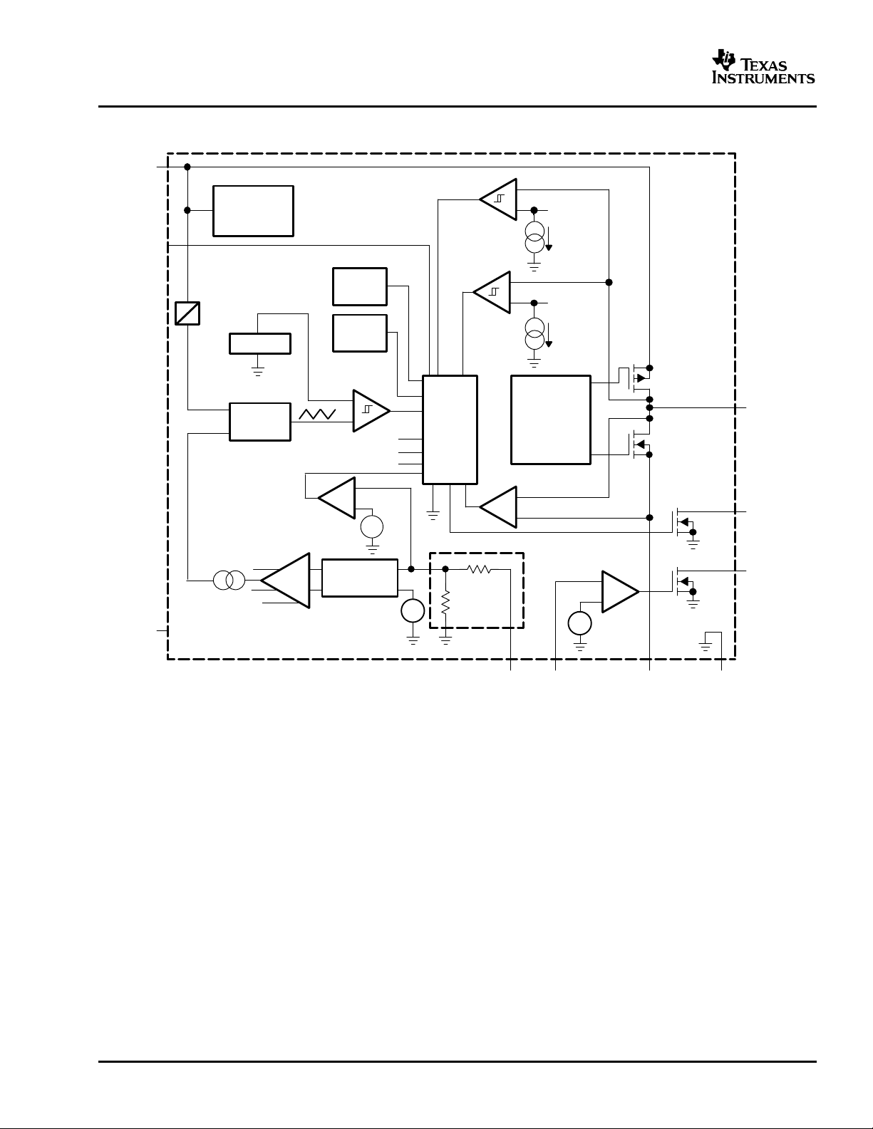
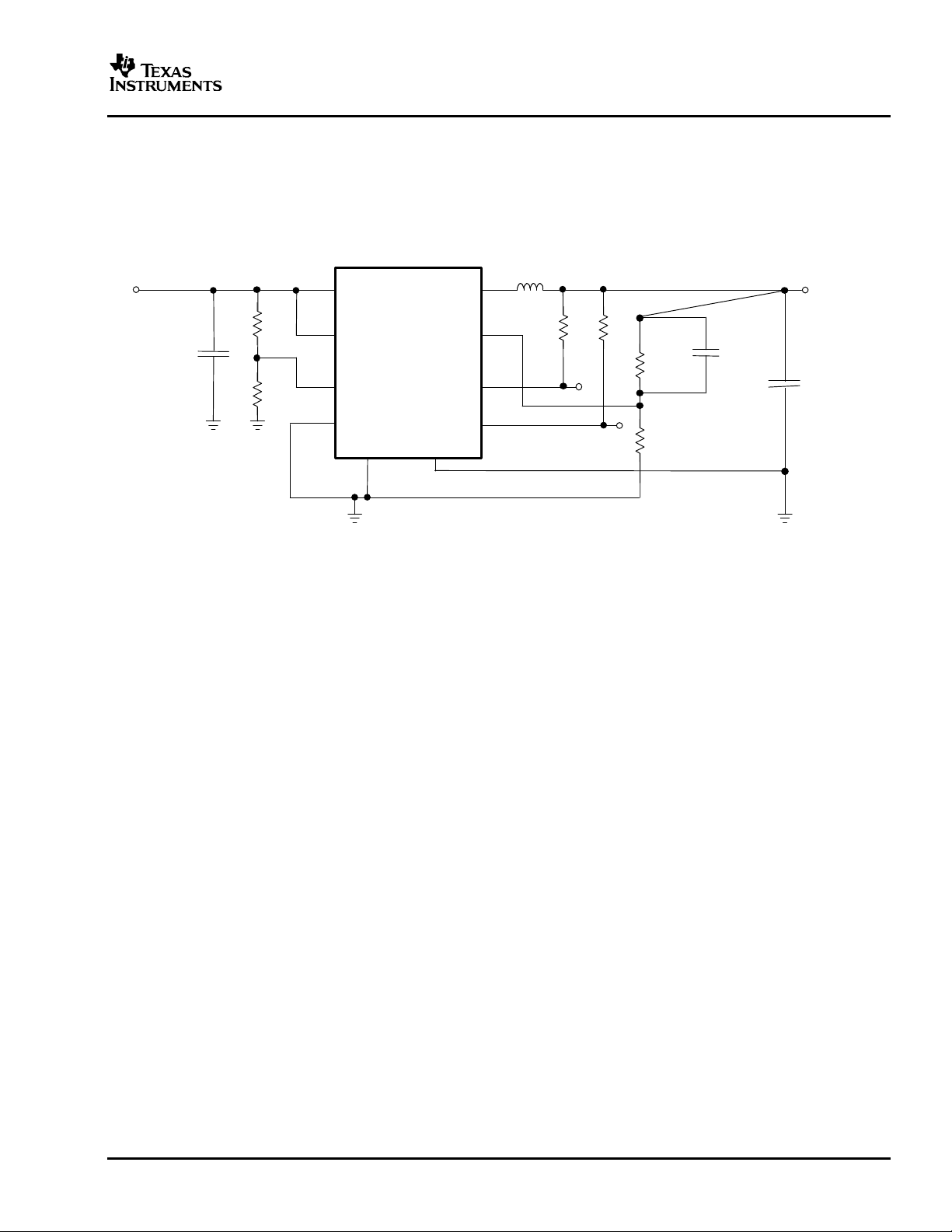
FB
PG
VIN
8
LBO
GND
SYNC
EN
LBI
PGND
TPS62052
SW
1
6
7
3
2
9
5
4
10
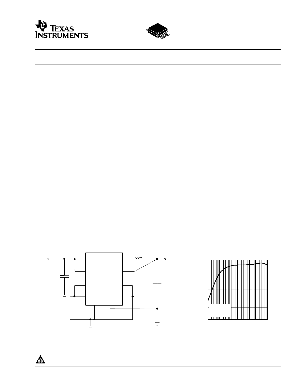
Ci = 10 µF
Co = 22 µF
VO = 1.5 V / 800 mA
L1 = 10 µHVI = 3.3 V to 10 V
TYPICAL APPLICATION CIRCUIT
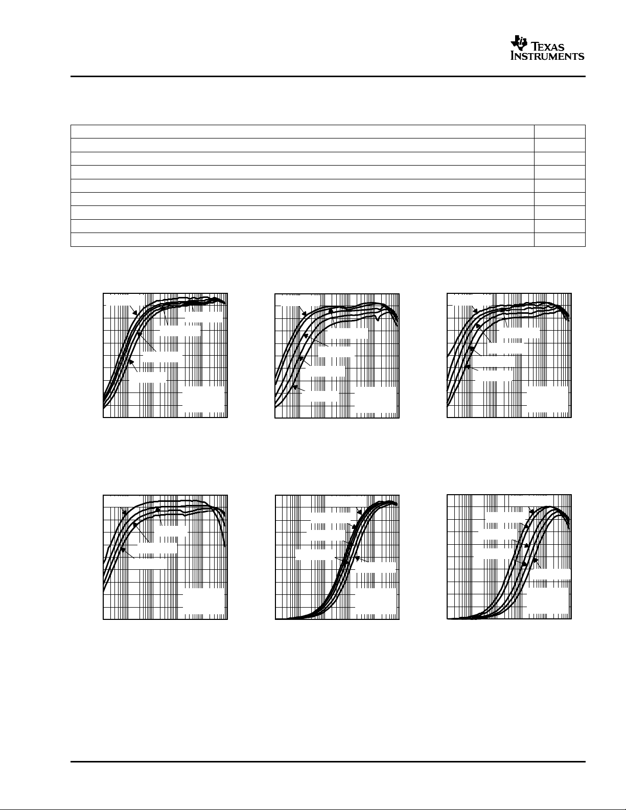
IO – Output Current – mA
50
30
10
0.01 0.1 1 10
Efficiency – %
60
70
TPS62050
EFFICIENCY
vs
OUTPUT CURRENT
100
100 1 k
80
20
0
40
90
V
I
= 7.2 V,
VO = 5 V,
SYNC = L
TPS62050, TPS62051
TPS62052, TPS62054, TPS62056
SLVS432D–SEPTEMBER 2002 – REVISED OCTOBER 2003
800-mA SYNCHRONOUSSTEP-DOWN CONVERTER
FEATURES DESCRIPTION
• High-Efficiency Synchronous Step-Down
Converter With up to95% Efficiency
• 12-A Quiescent Current (Typ) for systems powered from a 1-cell or 2-cell Li-Ion
• 2.7-V to 10-V OperatingInput Voltage Range
• Adjustable Output Voltage RangeFrom 0.7 V
to 6 V
• Fixed Output Voltage OptionsAvailable in
1.5 V, 1.8 V,and 3.3 V
• Synchronizable to External ClockSignal up to
1.2 MHz
• High Efficiency Over aWide Load Current
Range in Power-Save Mode
• 100% Maximum Duty Cyclefor Lowest
Dropout
• Low Noise Operation inForced Fixed
Frequency PWM Operation Mode
• Internal Softstart
• Overtemperature and Overcurrent Protected
• Available in 10-Pin MicrosmallOutline
Package MSOP
The TPS6205x devices are a family of high-efficiency
synchronous step-down dc/dc converters ideally suited
battery or from a 3-cell to 5-cell NiCd, NiMH, or alkaline
battery.
The TPS62050 is a synchronous PWM converter with
integrated N-channel and P-channel power MOSFET
switches. Synchronous rectification increases efficiency and reduces external component count. To
achieve highest efficiency over a wide load current
range, the converter enters a power-saving
pulse-frequency modulation (PFM) mode at light load
currents. Operating frequency is typically 850 kHz,
allowing the use of small inductor and capacitor values.
The device can be synchronized to an external clock
signal in the range of 600 kHz to 1.2 MHz. For low noise
operation, the converter can be programmed into
forced-fixed frequency in PWM mode. In shutdown
mode, the current consumption is reduced to less than
2 µA. The TPS6205x is available in the 10-pin (DGS)
micro-small outline package (MSOP) and operates
over an free air temperature range of -40°C to 85°C.
APPLICATIONS
• Cellular Phones
• Organizers, PDAs, and HandheldPCs
• Low Power DSP Supply
• Digital Cameras and HardDisks
MATHCAD is a trademark of Mathsoft Incorporated.
Please be aware that an important notice concerning availability, standard warranty, and use in critical applications of Texas Instruments
semiconductor products and disclaimers thereto appears at the end of this data sheet.
PRODUCTION DATA information is current as of publication date.
Products conform tospecifications per the terms ofTexas Instruments
standard warranty. Production processing does not necessarily includetestingof allparameters.
Copyright © 2002 – 2003, Texas Instruments Incorporated
www.ti.com
TPS62050, TPS62051
TPS62052, TPS62054, TPS62056
SLVS432D–SEPTEMBER 2002 – REVISED OCTOBER 2003
This integrated circuit can be damaged by ESD. Texas Instruments recommends that all integrated circuits be handled with
appropriate precautions. Failure to observe proper handling and installation procedures can cause damage. ESD damage can
range from subtle performance degradation to complete device failure. Precision integrated circuits may be more susceptible to
damage because very small parametric changes could cause the device not to meet its published specifications.
PACKAGE/ORDERING INFORMATION
PACKAGED DEVICES
PLASTIC MSOP
TPS62050DGS Adjustable 0.7 V to 6 V Standard BFM
TPS62051DGS Adjustable 0.7 V to 6 V Enhanced BGB
TPS62052DGS 1.5 V Standard BGC
TPS62054DGS 1.8 V Standard BGE
TPS62056DGS 3.3 V Standard BGG
(1)
The DGS packages are available taped and reeled. Add an R suffix to the device type (i.e., TPS62050DGSR) to order quantities of
2500 devices per reel.
(1)
(DGS)
ABSOLUTE MAXIMUM RATINGS
over operating free-air temperature range unless otherwise noted
Supply voltage, V
Voltage at EN, SYNC -0.3 V to V
Voltage at LBI, FB, LBO, PG -0.3 V to 7 V
Voltage at SW -0.3 V to 11 V
Output current, I
Maximum junction temperature, T
Operating free-air temperature range, T
Storage temperature range, T
Lead temperature 1,6 mm (1/16 inch) from case for 10 seconds 300°C
(1)
Stresses above these ratings may cause permanent damage. Exposure to absolute maximum conditions for extended periods may
degrade device reliability. These are stress ratings only, and functional operation of the device at these or any other conditions beyond
those specified is not implied.
(2)
The voltage at the SW pin is sampled in PFM mode 15 µs after the PMOS has switched off. During this time the voltage at SW is
limited to 7 V maximum. Therefore, the output voltage of the converter is limited to 7 V maximum.
I
O
J
stg
OUTPUT VOLTAGE LBI/LBO FUNCTIONALITY PACKAGE MARKING
(1)
TPS6205x
-0.3 V to 11 V
850 mA
150°C
A
-40°C to 85°C
-65°C to 150°C
I
(2)
PACKAGE DISSIPATION RATING
PACKAGE
10-PIN MSOP
(1)
The thermal resistance junction to ambient soldered onto a PCB of the 10-pin MSOP is 180°C/W.
(1)
TA≤ 25°C DERATING FACTOR TA= 70°C TA= 85°C
POWER RATING TA≤ 25°C POWER RATING POWER RATING
555 mW 5.56 mW/°C 305 mW 221 mW
RECOMMENDED OPERATING CONDITIONS
MIN NOM MAX UNIT
Supply voltage at V
Voltage at PG, LBO 6 V
Maximum output current 800
Operating junction temperature -40 125 °C
(1)
Assuming no thermal limitation
2
I
2.7 10 V
(1)
mA
www.ti.com
TPS62052, TPS62054, TPS62056
SLVS432D–SEPTEMBER 2002 – REVISED OCTOBER 2003
ELECTRICAL CHARACTERISTICS
VI=7.2 V, VO= 3.3 V, IO= 300 mA, EN = VI, TA=-40°C to 85°C unless otherwise noted
PARAMETER TEST CONDITIONS MIN TYP MAX UNIT
SUPPLY CURRENT
V
I
I
(Q)
I
(SD)
I
Q(LBI)
ENABLE
V
IH
V
IL
I
lkg
I
(EN)
V
(UVLO)
POWER SWITCH
r
DS(on)
r
DS(on)
POWER GOOD OUTPUT, LBI, LBO
V
(PG)
V
OL
V
(LBI)
V
(LBI,HYS)
I
lkg(LBI)
OSCILLATOR
f
S
f
(SYNC)
V
IH
V
IL
I
lkg
OUTPUT
V
O
V
(FB)
Input voltage range 2.7 10 V
Operating quiescent current 12 20 µA
Shutdown current µA
IO= 0 mA, SYNC = GND,
VI= 7.2 V
EN = GND 1.5 5
EN = GND, TA=25°C 1.5 3
Quiescent current with enhanced LBI EN = VI, LBI=GND,
comparator version. TPS62051 only
EN high level input voltage 1.3 V
EN low level input voltage 0.3 V
EN trip point hysteresis 100 mV
EN input leakage current EN = GND or VIN, VI=7.2 V 0.01 0.2 µA
EN input current 0.6 V ≤ V
≤ 4 V 2 µA
(EN)
Undervoltage lockout threshold 1.6 V
P-channel MOSFET on-resistance mΩ
VI≥ 5.4 V; IO= 300 mA 400 650
VI= 2.7 V; IO= 300 mA 600 850
P-channel MOSFET leakage current VDS= 10 V 1 µA
P-channel MOSFET current limit VI= 7.2V, VO= 3.3 V 1000 1200 1400 mA
N-channel MOSFET on-resistance mΩ
VI≥ 5.4 V; IO= 300 mA 300 450
VI= 2.7 V; IO= 300 mA 450 550
N-channel MOSFET leakage current VDS= 6 V 1 µA
Power good trip voltage Vml -2% V
Power good delay time
PG, LBO output low voltage 0.3 V
PG, LBO output leakage current 0.01 0.25 µA
VOramping positive 50 µs
VOramping negative 200
V
= 0.8 x VOnominal,
(FB)
I
= 1 mA
(sink)
V
= VOnominal,
(FB)
V
= V
(LBI)
I
Minimum supply voltage for valid power
good, LBO signal
Low battery input trip voltage Input voltage falling 1.21 V
Low battery input trip point accuracy 1.5%
Low battery input hysteresis 15 mV
LBI leakage current 0.01 0.1 µA
Oscillator frequency 600 850 1000 kHz
Synchronization range 600 1200 kHz
SYNC high level input voltage 1.5 V
SYNC low level input voltage 0.3 V
SYNC input leakage current SYNC = GND or VIN 0.01 0.1 µA
SYNC trip point hysteresis 100 mV
Duty cycle of external clock signal 20% 90%
Adjustable output voltage TPS62050,
range TPS62051
Feedback voltage 0.5 V
FB leakage current 0.02 0.1 µA
TPS62050,
TPS62051
TPS62050,
TPS62051
TPS62050, TPS62051
5 µA
2.3 V
0.7 6.0 V
3
www.ti.com
TPS62050, TPS62051
TPS62052, TPS62054, TPS62056
SLVS432D–SEPTEMBER 2002 – REVISED OCTOBER 2003
ELECTRICAL CHARACTERISTICS (continued)
VI=7.2 V, VO= 3.3 V, IO= 300 mA, EN = VI, TA=-40°C to 85°C unless otherwise noted
PARAMETER TEST CONDITIONS MIN TYP MAX UNIT
Feedback voltage TPS62050, VI= 2.7 V to 10 V,
tolerance TPS62051 0 mA< IO< 600 mA
TPS62052 -3% 3%
Fixed output voltage VI= 2.7 V to 10 V,
tolerance
Resistance of internal voltage divider
forfixed-voltage versions
Line regulation 5.2 mV/V
Load regulation VI= 7.2 V; IO= 10 mA to 600 mA 0.0045 %/mA
η Efficiency
Duty cycle range for main switches 100%
Minimum tontime for main switch 100 ns
Shutdown temperature 145 °C
Start-up time 1 ms
(1)
The worst case r
(1)
of the PMOS in 100% mode for an input voltage of 3.3 V is 0.75 Ω. This value can be used to determine the
DS(on)
TPS62054 -3% 3%
TPS62056 -3% 3%
minimum input voltage if the output current is less than 600 mA with the TPS62056.
VI= 2.7 V to 10 V,
0 mA< IO< 600 mA
0 mA< IO< 600 mA
VI= 3.75 V to 10 V,
0 mA< IO< 600 mA
VO= 3.3 V, VI= 5 V to 10 V,
IO= 600 mA
VI= 5 V; VO= 3.3 V; IO= 300 mA 93%
VI= 3.6 V; VO= 2.5 V; IO= 200 mA 93%
IO= 200 mA, VI= 5 V, Vo= 3.3 V,
Co= 22 µF, L = 10 µH
-3% 3%
700 1000 1300 kΩ
4

www.ti.com
www.ti.com
Undervoltage
Lockout
Bias Supply
_
+
+
–
REF
Current Limit Comparator
+
–
REF
I
(AVG)
Comparator
P-Channel
Power MOSFET
N-Channel
Power MOSFET
Driver
Shoot-Through
Logic
+
–
Load Comparator
Control
Logic
+
–
1.21 V
Soft Start
850 kHz
Oscillator
+
–
S
R
Comparator High
Comparator Low
Comparator High2
+
–
Compensation
R2
See Note
R1
V
REF
= 0.5 V
Comparator Low
Comparator Low2
Comparator High
Saw Tooth
Generator
V
I
V
(COMP)
Comparator
SW
PG
LBO
GNDPGNDLBIFB
V
I
EN
SKIP Comparator
Error Amp
SYNC
TPS62050, TPS62051
TPS62052, TPS62054, TPS62056
SLVS432D–SEPTEMBER 2002 – REVISED OCTOBER 2003
FUNCTIONAL BLOCK DIAGRAM
6
NOTE: For the adjustable versions (TPS62050, TPS62051), the internal feedback driver is disabled and the FB pin is
directly connected to the GM amplifier.
www.ti.com
PGND
FB
PG
VIN
8
LBO
GND
SYNC
EN
LBI
TPS62050
SW
1
6
7
3
2
9
5
4
10
L1 = 10 µH
VO = 5 V
R1 =
820 kΩ
C
(ff)
= 6.8 pF
R2 = 91 kΩ
Co = 22 µF
Ci = 10 µF
V
I
R5
130 kΩ
R6
100 kΩ
R3
1 MR41 M
TDK
C3216X5R1A106M
Taiyo Yuden
JMK316BJ226ML
WE PD 744 777 10
Quiescent Current Measurements and Efficiency Were Taken
With: R5 = Open, R4 = Open, LBI Connected to GND.
TPS62050, TPS62051
TPS62052, TPS62054, TPS62056
SLVS432D–SEPTEMBER 2002 – REVISED OCTOBER 2003
PARAMETER MEASUREMENT INFORMATION
All graphs were generated using the circuit as shown unless otherwise noted. For output voltages other than 5 V,
the fixed voltage versions are used. The resistors R1, R2, and the feedforward capacitor (Cff) are removed and
the feedback pin is directly connected to the output.
STANDARD CIRCUIT FOR ADJUSTABLEVERSION
7
www.ti.com
0
10
20
30
40
50
60
70
80
90
100
0.01 0.1 1 10 100 1 k
IL − Load Current − mA
Efficiency − %
VI = 5.5 V
VI = 6.5 V
VI = 7.2 V
VI = 8.4 V
VI = 10 V
SYNC = L
VO = 5 V
TA = 25°C
0
10
20
30
40
50
60
70
80
90
100
0.01 0.1 1 10 100 1 k
IL − Load Current − mA
Efficiency − %
VI = 2.7 V
VI = 3.3 V
VI = 5 V
SYNC = L
VO = 1.5 V
TA = 25°C
VI = 7.2 V
VI = 10 V
0
10
20
30
40
50
60
70
80
90
100
0.01 0.1 1 10 100 1 k
IL − Load Current − mA
Efficiency − %
VI = 2.7 V
VI = 3.3 V
VI = 5 V
SYNC = L
VO = 1.8 V
TA = 25°C
VI = 7.2 V
VI = 10 V
0
10
20
30
40
50
60
70
80
90
100
0.01 0.1 1 10 100 1 k
IL − Load Current − mA
Efficiency − %
VI = 2.7 V
SYNC = H
VO = 1.5 V
TA = 25°C
VI = 5 V
VI = 3.3 V
VI = 10 V
VI = 7.2 V
0
10
20
30
40
50
60
70
80
90
100
0.01 0.1 1 10 100 1 k
IL − Load Current − mA
Efficiency − %
VI = 3.5 V
VI = 5 V
SYNC = L
VO = 3.3 V
TA = 25°C
VI = 10 V
VI = 7.2 V
0
10
20
30
40
50
60
70
80
90
100
0.01 0.1 1 10 100 1 k
IL − Load Current − mA
Efficiency − %
VI = 5.5 V
SYNC = H
VO = 5 V
TA = 25°C
VI = 7.2 V
VI = 6.5 V
VI = 10 V
VI = 8.4 V
TPS62050, TPS62051
TPS62052, TPS62054, TPS62056
SLVS432D–SEPTEMBER 2002 – REVISED OCTOBER 2003
TYPICAL CHARACTERISTICS
TABLE OF GRAPHS
FIGURE
Efficiency vs load current 1 - 8
Switching frequency vs temperature 9
Output voltage ripple in SKIP mode 10
Output voltage ripple in PWM mode 11
Line transient response in PWM mode 12
Load transient 13
V
and IL(inductor current) in skip mode 14
(switch)
Start-up timing 15
TPS62050 TPS62052 TPS62054
EFFICIENCY EFFICIENCY EFFICIENCY
vs vs vs
LOAD CURRENT LOAD CURRENT LOAD CURRENT
8
Figure 1. Figure 2.
TPS62056 TPS62050 TPS62052
EFFICIENCY EFFICIENCY EFFICIENCY
vs vs vs
LOAD CURRENT LOAD CURRENT LOAD CURRENT
Figure 4. Figure 5.
Figure 3.
Figure 6.

www.ti.com
0
10
20
30
40
50
60
70
80
90
100
0.01 0.1 1 10 100 1 k
IL − Load Current − mA
Efficiency − %
VI = 3.5 V
SYNC = H
VO = 3.3 V
TA = 25°C
VI = 5 V
VI = 10 V
VI = 7.2 V
0
10
20
30
40
50
60
70
80
90
100
0.01 0.1 1 10 100 1 k
IL − Load Current − mA
Efficiency − %
VI = 2.7 V
SYNC = H
VO = 1.8 V
TA = 25°C
VI = 5 V
VI = 3.3 V
VI = 10 V
VI = 7.2 V
800
810
820
830
840
850
860
870
880
890
900
−40 −20 0 20 40 60 80 100
Switching Frequency − kHz
TA − Free-Air Temperature − °C
2.7 V
3.6 V
7.2 V
5 V
VI = 4.5 V to 5.5 V to 4.5 V
1 µs/div
10 mV/div 500 mv/div
V
O
1 µs/div
2 V/div
VI = 7.2 V
VO = 3.3 V
IO = 800 mA
Output Voltage
Voltage at SW Pin
10 mV/div
10 µs/div
2 V/div 10 mV/div
VI = 7.2 V, VO = 3.3 VOutput Voltage
Voltage at SW Pin
IO = 20 mA
VI = 5 V
RL = 2.7 Ω
EN
V
O
I
I
5 V/div
100 mA/div
200 µs/div
1 V/div
50 µs/div
500 mA/div
50 mV/div
VI = 5 V
VO = 3.3 V
Output Voltage
Load Step = 60 mA to 540 mA
Voltage at SW Pin
Inductor Current
VI = 5 V
IO = 100 mA
5 V/div
100 mA/div
5 µs/div
TYPICAL CHARACTERISTICS (continued)
TPS62054 TPS62056
EFFICIENCY EFFICIENCY SWITCHINGFREQUENCY
vs vs vs
LOAD CURRENT LOAD CURRENT FREE-AIR TEMPERATURE
TPS62050, TPS62051
TPS62052, TPS62054, TPS62056
SLVS432D–SEPTEMBER 2002 – REVISED OCTOBER 2003
Figure 7. Figure 8.
Figure 9.
OUTPUT VOLTAGE RIPPLE OUTPUT VOLTAGERIPPLE LINE TRANSIENT RESPONSE
IN SKIP MODE IN PWM MODE IN PWM MODE
Figure 10. Figure 11.
V
(SWITCH)
(INDUCTOR CURRENT)
AND I
L
Figure 12.
LOAD TRANSIENT IN SKIP MODE START-UP TIMING
Figure 13. Figure 14.
Figure 15.
9

www.ti.com
TPS62050, TPS62051
TPS62052, TPS62054, TPS62056
SLVS432D–SEPTEMBER 2002 – REVISED OCTOBER 2003
APPLICATION INFORMATION
Operation
The TPS6205x is a synchronous step-down converter that operates with a 850-kHz fixed frequency pulse width
modulation (PWM) at moderate to heavy load currents and enters the power-save mode at light load current.
During PWM operation the converter uses a unique fast response voltage mode control scheme with input
voltage feed forward to achieve good line and load regulation with the use of small ceramic input and output
capacitors. At the beginning of each clock cycle initiated by the clock signal (S), the P-channel MOSFET switch
is turned on and the inductor current ramps up until the voltage-comparator trips and the control logic turns the
switch off. Also the switch is turned off by the current limit comparator in case the current limit of the P-channel
switch is exceeded. After the dead time preventing current shoot through, the N-channel MOSFET rectifier is
turned on and the inductor current ramps down. The next cycle is initiated by the clock signal again, turning off
the N-channel rectifier and turning on the P-channel switch.
The error amplifier as well as the input voltage determines the rise time of the saw tooth generator; therefore,
any change in input voltage or output voltage directly controls the duty cycle of the converter giving a very good
line and load transient regulation.
Constant Frequency ModeOperation (SYNC = HIGH)
In the constant frequency mode, the output voltage is regulated by varying the duty cycle of the PWM signal in
the range of 100% to 10%. Connecting the SYNC pin to a voltage greater than 1.5 V forces the converter to
operate permanently in the PWM mode even at light or no load currents. The advantage is the converter
operates with a fixed switching frequency that allows simple filtering of the switching frequency for noise sensitive
applications. In this mode, the efficiency is lower compared to the power-save mode during light loads (see
Figure 16). The N-MOSFET of the devices stays on even when the current into the output drops to zero. This
prevents the device from going into discontinuous mode. The device transfers unused energy back to the input.
Therefore, there is no ringing at the output that usually occurs in the discontinuous mode. The duty cycle range
in constant frequency mode is 100% to 10%.
It is possible to switch from forced PWM mode to the power-save mode during operation by pulling the SYNC pin
low. The flexible configuration of the SYNC pin during operation of the device allows efficient power management
by adjusting the operation of the TPS6205x to the specific system requirements.
Power-Save Mode Operation(SYNC = LOW)
As the load current decreases, the converter enters the power-save mode operation. During power-save mode
the converter operates with reduced switching frequency in PFM and with a minimum quiescent current to
maintain high efficiency. Whenever the average output current goes below the skip threshold, the converter
enters the power-save mode. The average current depends on the input voltage. It is 100 mA at low input
voltages and up to 200 mA with maximum input voltage. The average output current must be below the threshold
for at least 32 clock cycles (tcy) to enter the power-save mode. During the power-save mode the output voltage is
monitored with a comparator. When the output voltage falls below the comp low threshold set to 0.8% above V
nominal, the P-channel switch turns on. The P-channel switch turns off as the peak switch current of typically 200
mA is reached. The N-channel rectifier turns on and the inductor current ramps down. As the inductor current
approaches zero, the N-channel rectifier is turned off and the switch is turned on starting the next pulse. When
the output voltage can not be reached with a single pulse, the device continues to switch with its normal
operating frequency, until the comparator detects the output voltage to be 1.6% above the nominal output
voltage. The converter wakes up again when the output voltage falls below the comp low threshold. This control
method reduces the quiescent current to typically to 12 µA and the switching frequency to a minimum achieving
the highest converter efficiency. Having these skip current thresholds 0.8% and 1.6% above the nominal output
voltage gives a lower absolute voltage drop during a load transient as anticipated with a standard converter
operating in this mode.
O
10

www.ti.com
, nominal
0.8%
1.6%
–1.6%
t
V
O
APPLICATION INFORMATION (continued)
Feedforward Capacitor
TPS62050, TPS62051
TPS62052, TPS62054, TPS62056
SLVS432D–SEPTEMBER 2002 – REVISED OCTOBER 2003
The feedforward capacitor, C
shown in Figure 20, improves the performance in SKIP mode. The comparator is
(ff)
faster, therefore, there is less voltage ripple at the output in SKIP mode. Use the values listed in Table 1. Larger
values decrease stability in fixed frequency PWM mode. If the TPS6205x is only operated in fixed frequency
PWM mode, the feedforward capacitor is not needed.
Figure 16. Power-Save ModeOutput Voltage Thresholds
The converter enters the fixed frequency PWM mode again as soon as the output voltage falls below the comp
low 2 threshold set to 1.6% below VO, nominal.
Soft-Start
The TPS6205x has an internal soft-start circuit that limits the inrush current during start-up. This prevents
possible voltage drops of the input voltage if a battery or a high impedance power source is connected to the
input of the TPS6205x.
The soft-start is implemented as a digital circuit increasing the switch current in steps of 200 mA, 400 mA, 800
mA and then the typical switch current limit of 1.2 A. Therefore the start-up time mainly depends on the output
capacitor and load current. Typical start-up time with a 22-µF output capacitor and a 200-mA load current is 1
ms.
100% Duty CycleLow Dropout Operation
The TPS6205x offers the lowest possible input to output voltage difference while still maintaining operation with
the use of the 100% duty cycle mode. In this mode, the P-channel switch is constantly turned on. This is
particularly useful in battery powered applications to achieve longest operation time by taking full advantage of
the whole battery voltage range, i.e. The minimum input voltage to maintain regulation depends on the load
current and output voltage and can be calculated as:
11

www.ti.com
VI(min) VO(max) IO(max)r
DS(on)
(max) R
L
IO(max) = Maximum output current plus inductor ripple current
r
DS(on)
(max) = Maximum P-Channel switch r
DS(on)
RL = DC resistance of the inductor
VO(max) = Nominal output voltage plus maximum output voltage tolerance
5 V
EN
VINVIN
Vt = 0.7 V
0 µA for VEN < 0.6 V
Typically 0.3 µA to 5 µAfor VEN < 4 V
Enable to Internal Circuitry
EN
VIN
ON
OFF
0.3 µA, min
R >1.3 V/0.3 µA
TPS6205x
TPS62050, TPS62051
TPS62052, TPS62054, TPS62056
SLVS432D–SEPTEMBER 2002 – REVISED OCTOBER 2003
APPLICATION INFORMATION (continued)
Enable and OvertemperatureProtection
Logic low on EN forces the TPS6205x into shutdown. In shutdown, the power switch, drivers, voltage reference,
oscillator, and all other functions are turned off. The supply current is reduced to less than 2 µA in the shutdown
mode. When the device is in thermal shutdown, the bandgap is forced to stay on even if the device is set into
shutdown by pulling EN to GND. As soon as the temperature drops below the threshold, the device automatically
starts again.
If an output voltage is present when the device is disabled, which could be an external voltage source or super
cap, the reverse leakage current is specified under electrical characteristics. Pulling the enable pin high starts up
the TPS6205x with the soft-start as described under the paragraph soft-start. If the EN pin is connected to any
voltage other than VIor GND, an increased leakage current of typically 10 µA and up to 20 µA can occur.
Figure 17. Internal Circuitof the ENABLE Pin
The EN pin can be used in a pushbutton configuration as shown in Figure 18. The external resistor to GND must
be capable of sinking 0.3 µA with a minimum voltage drop of 1.3 V to keep the system enabled when both
switches are open. When the ON-button is pressed, the device is enabled and the current through the external
resistor keeps the voltage level high to ensure that the device stays on when the ON-button is released. When
the OFF-button is pressed, the device is switched off and the current through the external resistor is zero. The
device therefore stays off even when the OFF-button is released.
Figure 18. Pushbutton Configurationfor the EN-Pin
12

www.ti.com
TPS62050, TPS62051
TPS62052, TPS62054, TPS62056
SLVS432D–SEPTEMBER 2002 – REVISED OCTOBER 2003
APPLICATION INFORMATION (continued)
Undervoltage Lockout
The undervoltage lockout circuit prevents the device from misoperation at low input voltages. It prevents the
converter from turning on the switch or rectifier MOSFET under undefined conditions.
Synchronization
If no clock signal is applied, the converter operates with a typical switching frequency of 850 kHz. It is possible to
synchronize the converter to an external clock within a frequency range from 600 kHz to 1200 kHz. The device
automatically detects the rising edge of the first clock and synchronizes to the external clock. If the clock signal is
stopped, the converter automatically switches back to the internal clock and continues operation. The switchover
is initiated if no rising edge on the SYNC pin is detected for a duration of four clock cycles. Therefore, the
maximum delay time can be 8.3 µs if the internal clock has its minimum frequency of 600 kHz. During this time,
there is no clock signal available. The device stops switching until the internal circuitry is switched to the internal
clock source.
When the device is switched between internal synchronization and external synchronization during operation, the
output voltage may show transient over/undershoot during switchover. The voltage transients are minimized by
using 850 kHz as an initial external frequency, and changing the frequency slowly (>1 ms) to the value desired.
The voltage drop at the output when the device is switched from external synchronization to internal
synchronization can be reduced by increasing the output capacitor value.
If the device is synchronized to an external clock, the power-save mode is disabled and the device stays in
forced PWM mode.
Connecting the SYNC pin to the GND pin enables the power-save mode. The converter operates in the PWM
mode at moderate to heavy loads and in the PFM mode during light loads maintaining high efficiency over a wide
load current range.
Power Good Comparator
The power good (PG) comparator has an open drain output capable of sinking typically 1 mA. The PG function is
only active when the device is enabled (EN = high). When the device is disabled (EN = low), the PG pin is pulled
to GND.
The PG output is only valid after a 250 µs delay after the device is enabled and the supply voltage is greater
than 2.7 V. Power good is low during the first 250 µs after shutdown and in shutdown.
The PG pin becomes active high when the output voltage exceeds typically 98.5% of its nominal value. Leave
the PG pin unconnected, or connect to GND when not used.
Low-Battery Detector (StandardVersion)
The low-battery output (LBO) is an open drain type which goes low when the voltage at the low battery input
(LBI) falls below the trip point of 1.21 V ±1.5%. The voltage at which the low-battery warning is issued is adjusted
with a resistive divider as shown in Figure 20. The sum of the resistors R1 and R2 is recommended to be in the
100-kΩ to 1-MΩ range for high efficiency at low output current. An external pullup resistor at LBO can either be
connected to OUT, or any other voltage rail in the voltage range of 0 V to 6 V. During start-up, the LBO output
signal is invalid for the first 500 µs. LBO is high impedance when the device is disabled. If the low-battery
comparator function is not used, connect LBI to ground. The low-battery detector is disabled when the device is
disabled. Leave the LBO pin unconnected, or connect to GND when not used.
13

www.ti.com
LBI
ENABLE
LBO
VIN
Bandgap
LBI
Comparator
Enable to Internal Circuitry
FB
PG
VIN
8
LBO
GND
SYNC
EN
LBI
PGND
TPS62051
SW
1
6
7
3
2
9
5
4
10
R3 R4 R1
R2
R5
R6
R7
1 Cell Li-lon
Ci = 10 µF
L1 = 10 µH
VO = 2.5 V / 600 mA
Co = 22 µF
C
(ff)
=
6.8 pF
TPS62050, TPS62051
TPS62052, TPS62054, TPS62056
SLVS432D–SEPTEMBER 2002 – REVISED OCTOBER 2003
APPLICATION INFORMATION (continued)
ENABLE/Low-Battery Detector (EnhancedVersion) TPS62051 Only
The TPS62051 offers an enhanced LBI functionality to provide a precise, user programmable undervoltage
shutdown. No additional supply voltage supervisor (SVS) is needed to provide this function.
When the enable (EN) pin is pulled high, only the internal bandgap voltage reference is switched on to provide a
reference source for the LBI comparator. As long as the voltage at LBI is less than the LBI trip point, all other
internal circuits are shut down, reducing the supply current to 5 µA. As soon as input voltage at LBI rises above
the LBI trip point of 1.21 V, the device is completely enabled and starts switching.
Figure 19. Block Diagramof ENABLE/LBI Functionality for TPS62051
The logic level of the LBO pin is not defined for the first 500 µs after EN is pulled high.
When the enhanced LBI is used to supervise the battery voltage and shut down the TPS62051 at low input
voltages, the battery voltage rises again when the current drops to zero. The implemented hysteresis on the LBI
pin may not be sufficient for all types of batteries. Figure 20 shows how an additional external hysteresis can be
implemented.
Figure 20. Enhanced LBIWith Increased Hysteresis
A MATHCAD™ file to calculate R7 can be downloaded from the product folder on the TI web.
14

www.ti.com
PGND
FB
PG
VIN
8
LBO
GND
SYNC
EN
LBI
TPS62050
SW
1
6
7
3
2
9
5
4
10
L1 = 10 µH
VO = 5 V
R1 =
820 kΩ
C
(ff)
= 6.8 pF
R2 = 91 kΩ
Co = 22 µF
Ci = 10 µF
V
I
R5
130 kΩ
R6
100 kΩ
R3
1 MR41 M
TDK
C3216X5R1A106M
Taiyo Yuden
JMK316BJ226ML
WE PD 744 777 10
Quiescent Current Measurements and Efficiency Were Taken
With: R5 = Open, R4 = Open, LBI Connected to GND.
VO V
FB
R1 R2
R2
R1 R2
V
O
V
FB
–R2
VFB 0.5V
TPS62050, TPS62051
TPS62052, TPS62054, TPS62056
SLVS432D–SEPTEMBER 2002 – REVISED OCTOBER 2003
APPLICATION INFORMATION (continued)
No Load Operation
If the converter operates in the forced PWM mode and there is no load connected to the output, the converter
regulates the output voltage by allowing the inductor current to reverse for a short period of time.
STANDARD CIRCUIT FORADJUSTABLE VERSION
Table 1. Values
NOMINAL OUTPUT VOLTAGE EQUATION POSSIBLERESISTOR COMBINATION TYPICAL FEEDBACK CAPACITOR
0.7 V R1 = 0.4 x R2 R1 = 270 k, R2 = 680 k C
1.2 V R1 = 1.4 x R2 R1 = 510 k, R2 = 360 k (1.21 V) C
1.5 V R1 = 2 x R2 R1 = 300 k, R2 = 150 k (1.50 V) C
1.8 V R1 = 2.6 x R2 R1 = 390 k, R2 = 150 k (1.80 V) C
2.5 V R1 = 4 x R2 R1 = 680 k, R2 = 169 k (2.51 V) C
3.3 V R1 = 5.6 x R2 R1 = 560 k, R2 = 100 k (3.30 V) C
5 V R1 = 9 x R2 R1 = 820 k, R2 = 91 k (5.0 V) C
= 22 pF
(ff)
= 6.8 pF
(ff)
= 6.8 pF
(ff)
= 6.8 pF
(ff)
= 6.8 pF
(ff)
= 6.8 pF
(ff)
= 6.8 pF
(ff)
15

www.ti.com
L1 = 10 µH
VO = 1.8 V / 600 mA
Co = 22 µF
Ci = 10 µF
VI = 2.7 V to 10 V
FB
PG
VIN
8
LBO
GND
SYNC
EN
LBI
PGND
TPS62054
SW
1
6
7
3
2
9
5
4
10
R3
R5
R6
R4
PGND
FB
PG
VIN
8
LBO
GND
SYNC
EN
LBI
TPS62050
SW
1
6
7
3
2
9
5
4
10
L1 = 10 µH
VO = 0.7 V / 600 mA
R1 = 270 kΩ
C
(ff)
= 22 pF
R2 = 680 kΩ
Co = 47 µF
Ci = 10 µF
VI = 2.7 V to 7 V

www.ti.com
IL V
O
1
V
O
V
I
L f
IL(max) IO(max)
IL
2
f = Switching frequency (850 kHz typical)
L = Inductor value
∆IL = Peak-to-peak inductor ripple current
IL(max) = Maximum inductor current
TPS62050, TPS62051
TPS62052, TPS62054, TPS62056
SLVS432D–SEPTEMBER 2002 – REVISED OCTOBER 2003
APPLICATION INFORMATION (continued)
INDUCTOR SELECTION
A 10-µH minimum inductor should be used with the TPS6205x. Values larger than 22 µH or smaller than 10 µH
may cause stability problems due to the internal compensation of the regulator. After choosing the inductor value
of typically 10 µH, two additional inductor parameter should be considered: the current rating of the inductor and
the dc resistance. The dc resistance of the inductance directly influences the efficiency of the converter.
Therefore, an inductor with lowest dc resistance should be selected for highest efficiency. In order to avoid
saturation of the inductor, the inductor should be rated at least for the maximum output current plus half the
inductor ripple current which is calculated as:
The highest inductor current occurs at maximum VIN . A more conservative approach is to select the inductor
current rating just for the maximum switch current of the TPS6205x which is 1.4 A maximum. See Table 2 for
inductors that have been tested for operation with the TPS6205x.
Table 2. Inductors
MANUFACTURER TYPE INDUCTANCE DC RESISTANCE SATURATION CURRENT
SLF7032T- 10 µH ±20%22 µH ±20%10 53 mΩ±20%110 1.4 A0.96 A1.3 A0.9 A
TDK 220M96SLF7045T- mΩ±20%61 mΩ±20%
Sumida
Coilcraft
Wuerth
100M1R4SLF7032T- µH ±20%22 µH ±20% mΩ±20%36
100M1R3SLF7045T-
100MR90
CDR74B 10 µH 70 mΩ 1.65 A
CDR74B 22 µH 130 mΩ 1.12 A
CDH74 10 µH 49 mΩ 1.8 A
CDH74 22 µH 110 mΩ 1.23 A
CDR63B 10 µH 140 mΩ 1 A
CDRH4D28 10 µH 128 mΩ 1 A
CDRH5D28 10 µH 48 mΩ 1.3 A
CDRH5D18 10 µH 92 mΩ 1.2 A
DT3316P-153 15 µH 60 mΩ 1.8 A
DT3316P-223 22 µH 84 mΩ 1.5 A
WE-PD 744 778 10 10 µH 72 mΩ 1.68 A
WE-PD 744 777 10 10 µH 49 mΩ 1.84 A
WE-PD 744 778 122 22 µH 190 mΩ 1.07A
WE-PD 744 777 122 22 µH 110 mΩ 1.23 A
17

www.ti.com
I
RMS(Co)
V
O
1–
V
O
V
I
L f
1
2 3
VO V
O
1
V
O
V
I
L f
1
8 Co f
R
ESR
I
RMS
IO(max)
V
O
V
I
1
V
O
V
I
TPS62050, TPS62051
TPS62052, TPS62054, TPS62056
SLVS432D–SEPTEMBER 2002 – REVISED OCTOBER 2003
APPLICATION INFORMATION (continued)
OUTPUT CAPACITOR SELECTION
The output capacitor should have a minimum value of 22µF. For best performance, a low ESR ceramic output
capacitor is needed.
For completeness, the RMS ripple current is calculated as:
The overall output ripple voltage is the sum of the voltage spike caused by the output capacitor ESR plus the
voltage ripple caused by charge and discharging the output capacitor:
The highest output voltage ripple occurs at the highest input voltage VI.
INPUT CAPACITOR SELECTION
Because the buck converter has a pulsating input current, a low ESR input capacitor is required for best input
voltage filtering and minimizing the interference with other circuits caused by high input voltage spikes. The input
capacitor should have a minimum value of 10 µF and can be increased without any limit for better input voltage
filtering. The input capacitor should be rated for the maximum input ripple current calculated as:
The worst case RMS ripple current occurs at D = 0.5 and is calculated as: I
good performance because of their low ESR value and they are less sensitive to voltage transients compared to
tantalum capacitors. Place the input capacitor as close as possible to the input pin of the IC for best
performance.
Table 3. Capacitors
MANUFACTURER PART NUMBER SIZE VOLTAGE CAPACITANCE TYPE
JMK212BJ106MG 0805 6.3 V 10 µF Ceramic
JMK316BJ106ML 1206 6.3 V 10 µF Ceramic
Taiyo Yuden
Kemet C1206C106M9PAC 1206 6.3 V 10 µF Ceramic
TDK C3216X5R0J226M 1206 6.3 V 22 µF Ceramic
(1)
Connect two in parallel.
JMK316BJ226ML 1206 6.3 V 22 µF Ceramic
LMK316BJ475ML 1206 10 V 4.7 µF
EMK316BJ475ML 1206 16 V 4.7 µF
EMK325BJ106KN-T 1210 16 V 10 µF Ceramic
C2012X5R0J106M 0805 6.3 V 10 µF Ceramic
C3216X5R1A106M 1206 10 V 10 µF Ceramic
= IO/2. Ceramic capacitors have a
RMS
(1)
(1)
Ceramic
Ceramic
18

www.ti.com
APPLICATION INFORMATION (continued)
Table 4. Capacitor Manufacturers
MANUFACTURER CAPACITOR TYPE INTERNET
Taiyo Yuden X7R/X5R ceramic www.t-yuden.com
TDK X7R/X5R ceramic www.component.tdk.com
Vishay X7R/X5R ceramic www.vishay.com
Kemet X7R/X5R ceramic www.kemet.com
TPS62050, TPS62051
TPS62052, TPS62054, TPS62056
SLVS432D–SEPTEMBER 2002 – REVISED OCTOBER 2003
19

PACKAGE OPTION ADDENDUM
www.ti.com
18-Sep-2008
PACKAGING INFORMATION
Orderable Device Status
(1)
Package
Type
Package
Drawing
Pins Package
Qty
Eco Plan
TPS62050DGS ACTIVE MSOP DGS 10 80 Green(RoHS &
no Sb/Br)
TPS62050DGSG4 ACTIVE MSOP DGS 10 80 Green(RoHS &
no Sb/Br)
TPS62050DGSR ACTIVE MSOP DGS 10 2500 Green (RoHS &
no Sb/Br)
TPS62050DGSRG4 ACTIVE MSOP DGS 10 2500 Green (RoHS &
no Sb/Br)
TPS62051DGS ACTIVE MSOP DGS 10 80 Green(RoHS &
no Sb/Br)
TPS62051DGSG4 ACTIVE MSOP DGS 10 80 Green(RoHS &
no Sb/Br)
TPS62051DGSR ACTIVE MSOP DGS 10 2500 Green (RoHS &
no Sb/Br)
TPS62051DGSRG4 ACTIVE MSOP DGS 10 2500 Green (RoHS &
no Sb/Br)
TPS62052DGS ACTIVE MSOP DGS 10 80 Green(RoHS &
no Sb/Br)
TPS62052DGSG4 ACTIVE MSOP DGS 10 80 Green(RoHS &
no Sb/Br)
TPS62052DGSR ACTIVE MSOP DGS 10 2500 Green (RoHS &
no Sb/Br)
TPS62052DGSRG4 ACTIVE MSOP DGS 10 2500 Green (RoHS &
no Sb/Br)
TPS62054DGS ACTIVE MSOP DGS 10 80 Green(RoHS &
no Sb/Br)
TPS62054DGSG4 ACTIVE MSOP DGS 10 80 Green(RoHS &
no Sb/Br)
TPS62054DGSR ACTIVE MSOP DGS 10 2500 Green (RoHS &
no Sb/Br)
TPS62054DGSRG4 ACTIVE MSOP DGS 10 2500 Green (RoHS &
no Sb/Br)
TPS62056DGS ACTIVE MSOP DGS 10 80 Green(RoHS &
no Sb/Br)
TPS62056DGSG4 ACTIVE MSOP DGS 10 80 Green(RoHS &
no Sb/Br)
TPS62056DGSR ACTIVE MSOP DGS 10 2500 Green (RoHS &
no Sb/Br)
TPS62056DGSRG4 ACTIVE MSOP DGS 10 2500 Green (RoHS &
no Sb/Br)
(1)
The marketing status values are defined as follows:
ACTIVE: Product device recommended for new designs.
LIFEBUY: TI has announced that the device will be discontinued, and a lifetime-buy period is in effect.
NRND: Not recommended for new designs. Device is in production to support existing customers, but TI does not recommend using this part in
a new design.
PREVIEW: Device has been announced but is not in production. Samples may or may not be available.
OBSOLETE: TI has discontinued the production of the device.
(2)
Lead/Ball Finish MSL Peak Temp
CU NIPDAU Level-1-260C-UNLIM
CU NIPDAU Level-1-260C-UNLIM
CU NIPDAU Level-1-260C-UNLIM
CU NIPDAU Level-1-260C-UNLIM
CU NIPDAU Level-1-260C-UNLIM
CU NIPDAU Level-1-260C-UNLIM
CU NIPDAU Level-1-260C-UNLIM
CU NIPDAU Level-1-260C-UNLIM
CU NIPDAU Level-1-260C-UNLIM
CU NIPDAU Level-1-260C-UNLIM
CU NIPDAU Level-1-260C-UNLIM
CU NIPDAU Level-1-260C-UNLIM
CU NIPDAU Level-1-260C-UNLIM
CU NIPDAU Level-1-260C-UNLIM
CU NIPDAU Level-1-260C-UNLIM
CU NIPDAU Level-1-260C-UNLIM
CU NIPDAU Level-1-260C-UNLIM
CU NIPDAU Level-1-260C-UNLIM
CU NIPDAU Level-1-260C-UNLIM
CU NIPDAU Level-1-260C-UNLIM
(3)
(2)
Eco Plan - The planned eco-friendly classification: Pb-Free (RoHS), Pb-Free (RoHS Exempt), or Green (RoHS & no Sb/Br) - please check
http://www.ti.com/productcontent for the latest availability information and additional product content details.
Addendum-Page 1

PACKAGE OPTION ADDENDUM
www.ti.com
TBD: The Pb-Free/Green conversion plan has not been defined.
Pb-Free (RoHS): TI's terms "Lead-Free" or "Pb-Free" mean semiconductor products that are compatible with the current RoHS requirements
for all 6 substances, including the requirement that lead not exceed 0.1% by weight in homogeneous materials. Where designed to be soldered
at high temperatures, TI Pb-Free products are suitable for use in specified lead-free processes.
Pb-Free (RoHS Exempt): This component has a RoHS exemption for either 1) lead-based flip-chip solder bumps used between the die and
package, or 2) lead-based die adhesive used between the die and leadframe. The component is otherwise considered Pb-Free (RoHS
compatible) as defined above.
Green (RoHS & no Sb/Br): TI defines "Green" to mean Pb-Free (RoHS compatible), and free of Bromine (Br) and Antimony (Sb) based flame
retardants (Br or Sb do not exceed 0.1% by weight in homogeneous material)
(3)
MSL, Peak Temp. -- The Moisture Sensitivity Level rating according to the JEDEC industry standard classifications, and peak solder
temperature.
Important Information and Disclaimer:The information provided on this page represents TI's knowledge and belief as of the date that it is
provided. TI bases its knowledge and belief on information provided by third parties, and makes no representation or warranty as to the
accuracy of such information. Efforts are underway to better integrate information from third parties. TI has taken and continues to take
reasonable steps to provide representative and accurate information but may not have conducted destructive testing or chemical analysis on
incoming materials and chemicals. TI and TI suppliers consider certain information to be proprietary, and thus CAS numbers and other limited
information may not be available for release.
In no event shall TI's liability arising out of such information exceed the total purchase price of the TI part(s) at issue in this document sold by TI
to Customer on an annual basis.
18-Sep-2008
Addendum-Page 2

PACKAGE MATERIALS INFORMATION
www.ti.com
TAPE AND REEL INFORMATION
6-Nov-2008
*All dimensions are nominal
Device Package
Type
TPS62050DGSR MSOP DGS 10 2500 330.0 12.4 5.2 3.3 1.6 8.0 12.0 Q1
TPS62051DGSR MSOP DGS 10 2500 330.0 12.4 5.2 3.3 1.6 8.0 12.0 Q1
TPS62052DGSR MSOP DGS 10 2500 330.0 12.4 5.2 3.3 1.6 8.0 12.0 Q1
TPS62054DGSR MSOP DGS 10 2500 330.0 12.4 5.2 3.3 1.6 8.0 12.0 Q1
TPS62056DGSR MSOP DGS 10 2500 330.0 12.4 5.2 3.3 1.6 8.0 12.0 Q1
Package
Drawing
Pins SPQ Reel
Diameter
(mm)
Reel
Width
W1 (mm)
A0 (mm) B0 (mm) K0 (mm) P1
(mm)W(mm)
Pin1
Quadrant
Pack Materials-Page 1

PACKAGE MATERIALS INFORMATION
www.ti.com
6-Nov-2008
*All dimensions are nominal
Device Package Type Package Drawing Pins SPQ Length (mm) Width (mm) Height (mm)
TPS62050DGSR MSOP DGS 10 2500 338.1 340.5 21.1
TPS62051DGSR MSOP DGS 10 2500 338.1 340.5 21.1
TPS62052DGSR MSOP DGS 10 2500 338.1 340.5 21.1
TPS62054DGSR MSOP DGS 10 2500 338.1 340.5 21.1
TPS62056DGSR MSOP DGS 10 2500 338.1 340.5 21.1
Pack Materials-Page 2


IMPORTANT NOTICE
Texas Instruments Incorporated and its subsidiaries (TI) reserve the right to make corrections, modifications, enhancements, improvements,
and other changes to its products and services at any time and to discontinue any product or service without notice. Customers should
obtain the latest relevant information before placing orders and should verify that such information is current and complete. All products are
sold subject to TI’s terms and conditions of sale supplied at the time of order acknowledgment.
TI warrants performance of its hardware products to the specifications applicable at the time of sale in accordance with TI’s standard
warranty. Testing and other quality control techniques are used to the extent TI deems necessary to support this warranty. Except where
mandated by government requirements, testing of all parameters of each product is not necessarily performed.
TI assumes no liability for applications assistance or customer product design. Customers are responsible for their products and
applications using TI components. To minimize the risks associated with customer products and applications, customers should provide
adequate design and operating safeguards.
TI does not warrant or represent that any license, either express or implied, is granted under any TI patent right, copyright, mask work right,
or other TI intellectual property right relating to any combination, machine, or process in which TI products or services are used. Information
published by TI regarding third-party products or services does not constitute a license from TI to use such products or services or a
warranty or endorsement thereof. Use of such information may require a license from a third party under the patents or other intellectual
property of the third party, or a license from TI under the patents or other intellectual property of TI.
Reproduction of TI information in TI data books or data sheets is permissible only if reproduction is without alteration and is accompanied
by all associated warranties, conditions, limitations, and notices. Reproduction of this information with alteration is an unfair and deceptive
business practice. TI is not responsible or liable for such altered documentation. Information of third parties may be subject to additional
restrictions.
Resale of TI products or services with statements different from or beyond the parameters stated by TI for that product or service voids all
express and any implied warranties for the associated TI product or service and is an unfair and deceptive business practice. TI is not
responsible or liable for any such statements.
TI products are not authorized for use in safety-critical applications (such as life support) where a failure of the TI product would reasonably
be expected to cause severe personal injury or death, unless officers of the parties have executed an agreement specifically governing
such use. Buyers represent that they have all necessary expertise in the safety and regulatory ramifications of their applications, and
acknowledge and agree that they are solely responsible for all legal, regulatory and safety-related requirements concerning their products
and any use of TI products in such safety-critical applications, notwithstanding any applications-related information or support that may be
provided by TI. Further, Buyers must fully indemnify TI and its representatives against any damages arising out of the use of TI products in
such safety-critical applications.
TI products are neither designed nor intended for use in military/aerospace applications or environments unless the TI products are
specifically designated by TI as military-grade or "enhanced plastic." Only products designated by TI as military-grade meet military
specifications. Buyers acknowledge and agree that any such use of TI products which TI has not designated as military-grade is solely at
the Buyer's risk, and that they are solely responsible for compliance with all legal and regulatory requirements in connection with such use.
TI products are neither designed nor intended for use in automotive applications or environments unless the specific TI products are
designated by TI as compliant with ISO/TS 16949 requirements. Buyers acknowledge and agree that, if they use any non-designated
products in automotive applications, TI will not be responsible for any failure to meet such requirements.
Following are URLs where you can obtain information on other Texas Instruments products and application solutions:
Products Applications
Amplifiers amplifier.ti.com Audio www.ti.com/audio
Data Converters dataconverter.ti.com Automotive www.ti.com/automotive
DSP dsp.ti.com Broadband www.ti.com/broadband
Clocks and Timers www.ti.com/clocks Digital Control www.ti.com/digitalcontrol
Interface interface.ti.com Medical www.ti.com/medical
Logic logic.ti.com Military www.ti.com/military
Power Mgmt power.ti.com Optical Networking www.ti.com/opticalnetwork
Microcontrollers microcontroller.ti.com Security www.ti.com/security
RFID www.ti-rfid.com Telephony www.ti.com/telephony
RF/IF and ZigBee® Solutions www.ti.com/lprf Video & Imaging www.ti.com/video
Mailing Address: Texas Instruments, Post Office Box 655303, Dallas, Texas 75265
Copyright © 2008, Texas Instruments Incorporated
Wireless www.ti.com/wireless
 Loading...