

Texas Instruments TPS62040DGQ, TPS62040DRC, TPS62042DGQ, TPS62042DRC, TPS62043DGQ Schematic [ru]
...
www.ti.com
SLVS463B − JUNE 2003 − REVISED OCTOBER 2005
1.2 A/1.25 MHz, HIGH-EFFICIENCY STEP-DOWN CONVERTER
TPS62040
TPS62042, TPS62043
TPS62044, TPS62046
FEATURES
D Up to 95% Conversion Efficiency
D Typical Quiescent Current: 18 µA
D Load Current: 1.2 A
D Operating Input Voltage Range: 2.5 V to 6.0 V
D Switching Frequency: 1.25 MHz
D Adjustable and Fixed Output Voltage
D Power Save Mode Operation at Light load
Currents
D 100% Duty Cycle for Lowest Dropout
D Internal Softstart
D Dynamic Output Voltage Positioning
D Thermal Shutdown
D Short-Circuit Protection
D 10 Pin MSOP PowerPad™ Package
D 10 Pin QFN 3 X 3 mm Package
APPLICATIONS
D PDA, Pocket PC and Smart Phones
D USB Powered Modems
D CPUs and DSPs
D PC Cards and Notebooks
D xDSL Applications
D Standard 5-V to 3.3-V Conversion
DESCRIPTION
The TPS6204x family of devices are high efficiency
synchronous step-down dc-dc converters optimized for
battery powered portable applications. The devices are
ideal for portable applications powered by a single Li-Ion
battery cell or by 3-cell NiMH/NiCd batteries. With an
output voltage range from 6.0 V down to 0.7 V, the devices
support low voltage DSPs and processors in PDAs,
pocket PCs, as well as notebooks and subnotebook
computers. The TPS6204x operates at a fixed switching
frequency of 1.25 MHz and enters the power save mode
operation at light load currents to maintain high efficiency
over the entire load current range. For low noise
applications, the devices can be forced into fixed
frequency PWM mode by pulling the MODE pin high. The
TPS6204x supports up to 1.2-A load current.
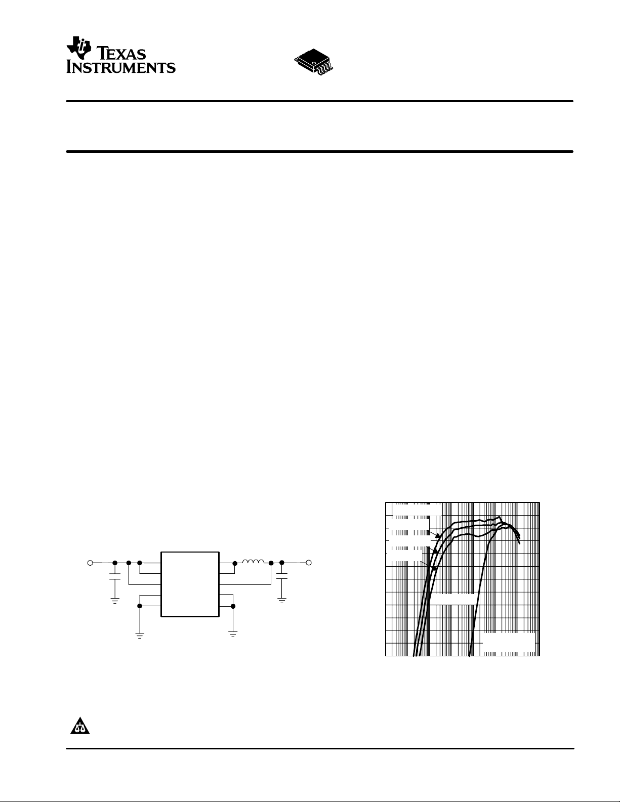
Typical Application Circuit 1.2-A Output Current
2
3
1
6
4
VIN
VIN
EN
MODE
GND
TPS6204x
PGND
PGND
SW
SW
FB
L1
6.2 µH
8
7
5
10
9
0.7 V to V
V
I
2.5 V to 6 V
C1
22 µF
Please be aware that an important notice concerning availability, standard warranty, and use in critical applications of Texas Instruments
semiconductor products and disclaimers thereto appears at the end of this data sheet.
PowerPAD is a trademark of Texas Instruments.
PRODUCTION DATA information is current as of publication date. Products
conform to specifications per the terms of Texas Instruments standard warranty.
Production processing does not necessarily include testing of all parameters.
V
C2
22 µF
O
/1.2 A
I
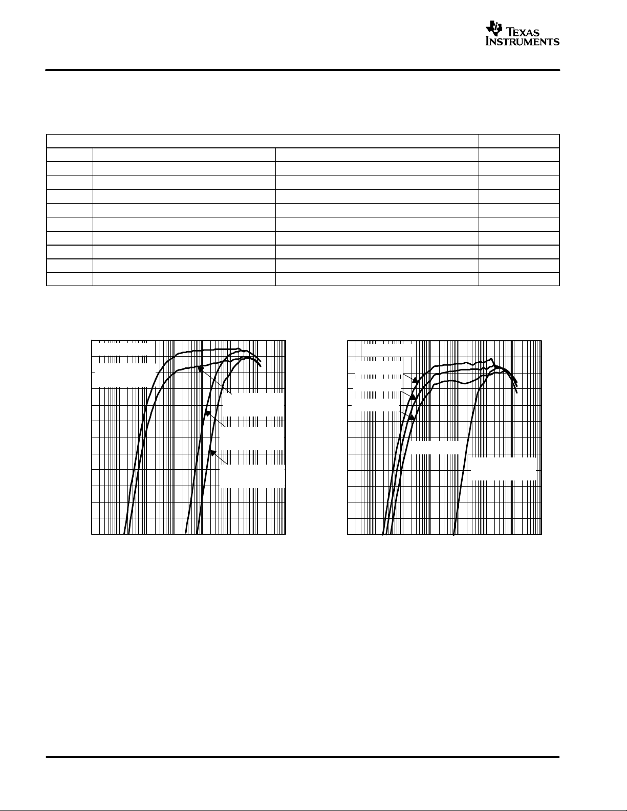
EFFICIENCY
vs
100
VO = 1.8 V
95
VI = 2.7 V
90
VI = 3.6 V
85
80
VI = 5 V
75
70
65
Efficiency − %
60
55
50
45
40
0 0.01 0.1 1 10 100 1 k 10 k
Copyright © 2003 − 2005, Texas Instruments Incorporated
LOAD CURRENT
MODE = Low
VI = 3.6 V
MODE = High
IL − Load Current − mA

TPS62040
40 C to 85 C
TPS62042, TPS62043
TPS62044, TPS62046
SLVS463B − JUNE 2003 − REVISED OCTOBER 2005
These devices have limited built-in ESD protection. The leads should be shorted together or the device placed in conductive foam during
storage or handling to prevent electrostatic damage to the MOS gates.
ORDERING INFORMATION
T
A
VOLTAGE OPTIONS
MSOP
Adjustable TPS62040DGQ TPS62040DRC BBI BBO
1.5 V TPS62042DGQ TPS62042DRC BBL BBS
−40°C to 85°C
1.6 V TPS62043DGQ TPS62043DRC BBM BBT
1.8 V TPS62044DGQ TPS62044DRC BBN BBU
3.3 V TPS62046DGQ TPS62046DRC BBQ BBW
(1)
The DGQ package is available in tape and reel. Add R suffix (DGQR) to order quantities of 2500 parts per reel.
(2)
The DRC package is available in tape and reel. Add R suffix (DRCR) to order quantities of 3000 parts per reel.
PACKAGE PACKAGE MARKING
(1)
QFN
(2)
www.ti.com
MSOP QFN
ABSOLUTE MAXIMUM RATINGS
over operating free-air temperature range unless otherwise noted
Supply voltage VIN
Voltages on EN, MODE, FB, SW
(2)
(2)
Continuous power dissipation See Dissipation Rating Table
Operating junction temperature range −40°C to 150°C
Storage temperature range −65°C to 150°C
Lead temperature (soldering, 10 sec) 260°C
(1)
Stresses beyond those listed under “absolute maximum ratings” may cause permanent damage to the device. These are stress ratings only, and
functional operation of the device at these or any other conditions beyond those indicated under recommended operating conditions is not implied.
Exposure to absolute-maximum-rated conditions for extended periods may affect device reliability.
(2)
All voltage values are with respect to network ground terminal.
(1)
UNITS
−0.3 V to 7 V
−0.3 V to VCC +0.3 V
PACKAGE DISSIPATION RATINGS
PACKAGE R
MSOP 60°C/W 1.67 W 917 mW 667 mW
QFN 48.7°C/W 2.05 W 1.13 W 821 mW
(1)
The thermal resistance, R
(1)
Q
JA
is based on a soldered PowerPAD using thermal vias.
Θ
JA
TA ≤ 25°C
POWER RATING
TA = 70°C
POWER RATING
TA = 85°C
POWER RATING
RECOMMENDED OPERATING CONDITIONS
MIN TYP MAX UNIT
V
Supply voltage 2.5 6.0 V
I
V
Output voltage range for adjustable output voltage version 0.7 V
O
I
Output current 1.2 A
O
L Inductor
C
I
C
O
T
A
T
J
(1)
Refer to application section for further information
(1)
Input capacitor
Output capacitor
(1)
(1)
Operating ambient temperature −40 85 °C
Operating junction temperature −40 125 °C
6.2 µH
22 µF
22 µF
I
V
2
www.ti.com
TPS62040
TPS62042, TPS62043
TPS62044, TPS62046
SLVS463B − JUNE 2003 − REVISED OCTOBER 2005
ELECTRICAL CHARACTERISTICS
VI = 3.6 V, VO = 1.8 V, IO = 600 mA, EN = VIN, TA = −40°C to 85°C, typical values are at TA = 25°C (unless otherwise noted)
SUPPLY CURRENT
PARAMETER TEST CONDITIONS MIN TYP MAX UNIT
V
I
I
(Q)
I
SD
V
UVLO
ENABLE AND MODE
V
EN
V
EN
I
EN
V
(MODE)
V
(MODE)
I
(MODE)
POWER SWITCH
r
DS(ON)
I
lkg(P)
r
DS(ON)
I
Ikg(N)
I
L
OSCILLATOR
f
S
OUTPUT
V
O
V
ref
V
FB
V
O
I
Ikg(SW)
f Short circuit switching frequency V
(1)
The line and load regulations are digitally controlled to assure an output voltage accuracy of ±3%.
Input voltage range 2.5 6.0 V
Operating quiescent current IO = 0 mA, device is not switching 18 35 µA
Shutdown supply current EN = GND 0.1 1 µA
Under−voltage lockout threshold 1.5 2.3 V
EN high level input voltage 1.4 V
EN low level input voltage 0.4 V
EN input bias current EN = GND or VIN 0.01 1.0 µA
MODE high level input voltage 1.4 V
MODE low level input voltage 0.4 V
MODE input bias current MODE = GND or VIN 0.01 1.0 µA
P-channel MOSFET on−resistance VI = VGS = 3.6 V 115 210 mΩ
P-channel MOSFET on−resistance VI = VGS = 2.5 V 145 270 mΩ
P-channel leakage current VDS = 6.0 V 1 µA
N-channel MOSFET on−resistance VI = VGS = 3.6 V 85 200 mΩ
N-channel MOSFET on−resistance VI = VGS = 2.5 V 115 280 mΩ
N-channel leakage current VDS = 6.0 V 1 µA
P-channel current limit 2.5 V < VI< 6.0 V 1.5 1.85 2.2 A
Thermal shutdown 150 °C
V
= 0.5 V 1 1.25 1.5 MHz
Oscillator frequency
FB
V
= 0 V 625 kHz
FB
Adjustable output voltage range TPS62040 0.7 V
Reference voltage 0.5 V
Feedback voltage
Fixed output voltage
Line regulation
Load regulation
(1)
(1)
TPS62040
Adjustable
TPS62042
1.5V
TPS62043
1.6V
TPS62044
1.8V
TPS62046
3.3V
VI = 2.5 V to 6.0 V; IO= 0 mA
VI = 2.5 V to 6.0 V; 0 mA ≤ I
VI = 2.5 V to 6.0 V; I
VI = 2.5 V to 6.0 V; 0 mA ≤ I
VI = 2.5 V to 6.0 V; I
VI = 2.5 V to 6.0 V; 0 mA ≤ I
VI = 2.5 V to 6.0 V; I
VI = 2.5 V to 6.0 V; 0 mA ≤ I
VI = 3.6 V to 6.0 V; I
VI = 3.6 V to 6.0 V; 0 mA ≤ I
VI = VO + 0.5 V (min. 2.5 V) to 6.0 V,
IO = 10 mA
IO = 10 mA to 1200 mA 0 %/mA
Leakage current into SW pin VI>VO, 0 V ≤ Vsw ≤ V
Reverse leakage current into pin SW V
= open; EN = GND; V
I
= 0 V 625 kHz
FB
≤ 1.2 A
O
= 0 mA
O
O
O
O
≤ 1.2 A
O
= 0 mA
≤ 1.2 A
O
= 0 mA
≤ 1.2 A
O
= 0 mA
≤ 1.2 A
O
I
= 6.0 V 0.1 1 µA
SW
0%
−3%
0%
−3%
0%
−3%
0%
−3%
0%
−3%
0.1 1 µA
(1)
V
IN
3%
3%
3%
3%
3%
3%
3%
3%
3%
3%
0 %/V
3
TPS62040
TPS62042, TPS62043
TPS62044, TPS62046
SLVS463B − JUNE 2003 − REVISED OCTOBER 2005
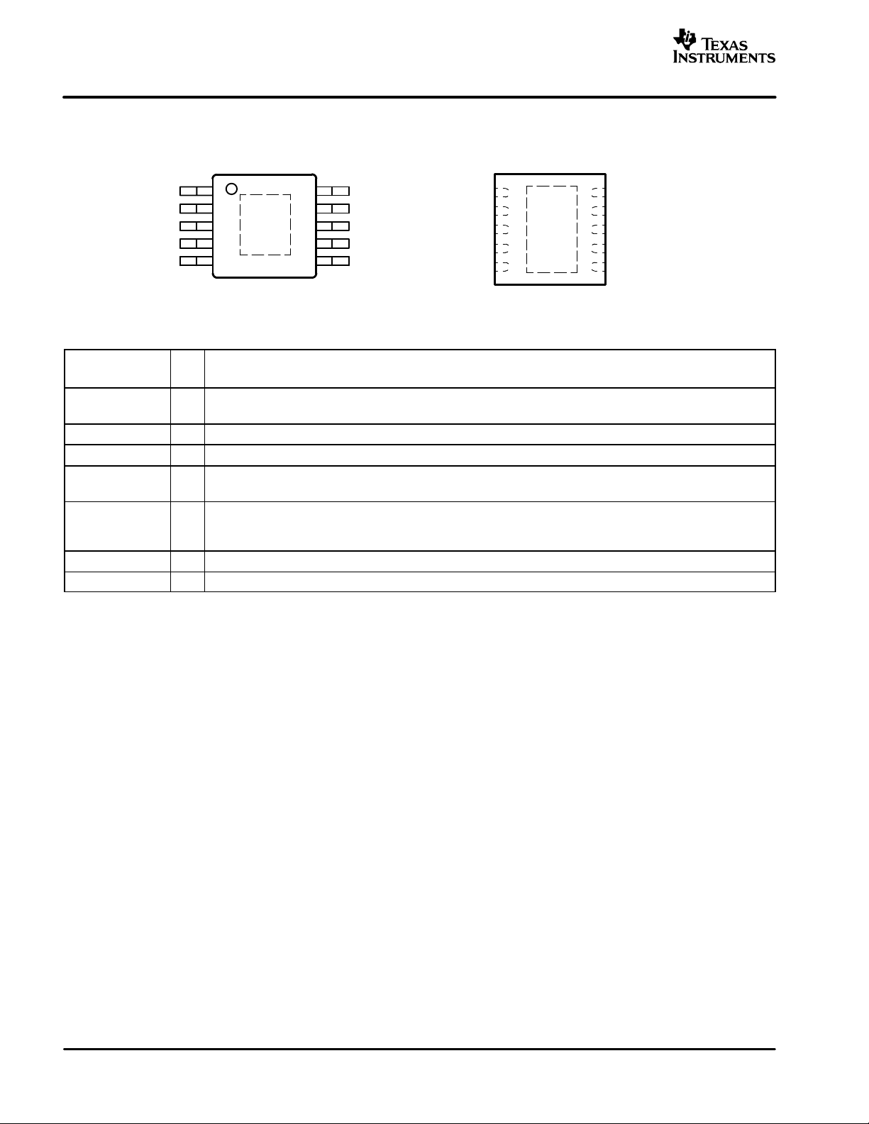
PIN ASSIGNMENTS
www.ti.com
DGQ PACKAGE
(TOP VIEW)
EN
VIN
VIN
GND
FB
NOTE:The PowerPAD must be connected to GND.
1
2
3
4
5
10
9
8
7
6
PGND
PGND
SW
SW
MODE
GND
EN
VIN
VIN
FB
DRC PACKAGE
(TOP VIEW)
1
2
3
4
5
10
PGND
9
PGND
8
SW
7
SW
6
MODE
Terminal Functions
TERMINAL
NAME NO.
EN 1 I Enable. Pulling EN to ground forces the device into shutdown mode. Pulling EN to VI enables the device. EN should
VIN 2,3 I Supply voltage input
GND 4 Analog ground
FB 5 I Feedback pin. Connect FB directly to the output if the fixed output voltage version is used. For the adjustable version
MODE 6 I Pulling the MODE pin high allows the device to be forced into fixed frequency operation. Pulling the MODE pin to low
SW 7,8 I/O This is the switch pin of the converter and is connected to the drain of the internal power MOSFETs
PGND 9,10 Power ground
I/O DESCRIPTION
not be left floating and must be terminated.
an external resistor divider is connected to this pin. The internal voltage divider is disabled for the adjustable version.
enables the power save mode where the device operates in fixed frequency PWM mode at high load currents and
in PFM mode (pulse frequency modulation) at light load currents.
4
www.ti.com
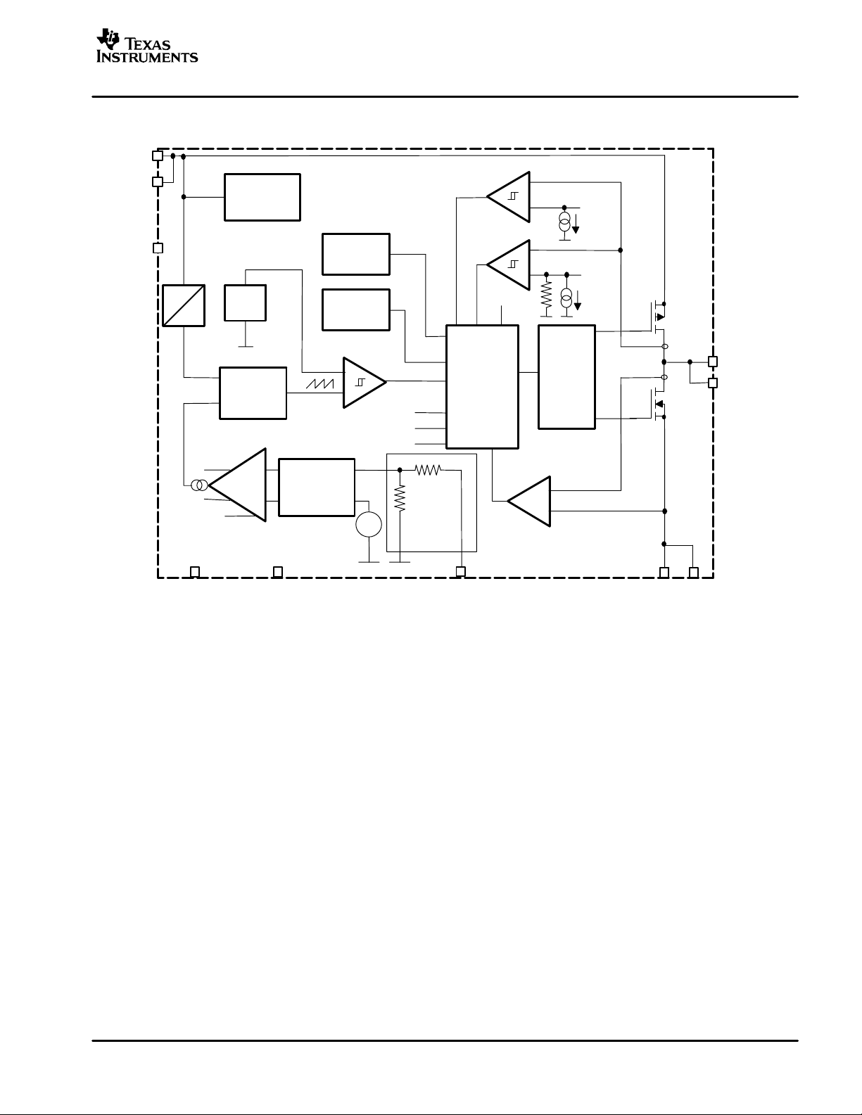
FUNCTIONAL BLOCK DIAGRAM
VIN
VIN
Undervoltage
Lockout
Bias supply
SLVS463B − JUNE 2003 − REVISED OCTOBER 2005
Current limit Comparator
+
−
Ref
TPS62040
TPS62042, TPS62043
TPS62044, TPS62046
EN
V
I
Comp High
Comp Low
Comp Low 2
Vcomp
Saw Tooth
Generator
−
Gm
+
Compensation
Vref = 0.5 V
GNDMODE
Soft
Start
1.25 MHz
Oscillator
Comparator
+
−
+
−
S
R
Comp High
Comp Low
Comp Low 2
R1
R2
+
SkipComparator
−
MODE
Control Logic
FB PGND
For the Adjustable Version the FB Pin Is
Directly Connected to the Gm Amplifier
Shoot−thru
LoadComparator
+
−
Ref
Driver
Logic
P−Channel
Power MOSFET
SW
SW
N−Channel
Power MOSFET
PGND
5
TPS62040
TPS62042, TPS62043
TPS62044, TPS62046
SLVS463B − JUNE 2003 − REVISED OCTOBER 2005
TYPICAL CHARACTERISTICS
TABLE OF GRAPHS
η Efficiency vs Load current 1, 2, 3
η Efficiency vs Input voltage 4
I
Q
f
s
r
DS(on)
r
DS(on)
Quiescent current vs Input voltage 5, 6
Switching frequency vs Input voltage 7
P-Channel r
N-Channel rectifier r
Load transient response 10
PWM operation 11
Power save mode 12
Start-up 13
DS(on)
) vs Input voltage 9
DS(on
vs Input voltage 8
www.ti.com
FIGURE
100
VO = 3.3 V
95
90
MODE = Low
85
80
75
70
65
Efficiency − %
60
55
50
45
40
0 0.01 0.1 1
EFFICIENCY
LOAD CURRENT
VI = 3.6 V
IL − Load Current − mA
Figure 1
vs
VI = 5 V
MODE = Low
VI = 3.6 V
MODE = High
VI = 5 V
MODE = High
10 100 1 k 10 k
EFFICIENCY
vs
LOAD CURRENT
Efficiency − %
100
95
90
85
80
75
70
65
60
55
50
45
40
VO = 1.8 V
VI = 2.7 V
VI = 3.6 V
VI = 5 V
MODE = Low
VI = 3.6 V
MODE = High
0 0.01 0.1 1 10 100 1 k 10 k
IL − Load Current − mA
Figure 2
6
www.ti.com
TPS62040
TPS62042, TPS62043
TPS62044, TPS62046
SLVS463B − JUNE 2003 − REVISED OCTOBER 2005
EFFICIENCY
vs
LOAD CURRENT
100
VO = 1.5 V
95
90
85
80
75
70
65
Efficiency − %
60
55
50
45
40
0 0.01 0.1 1 10 100 1 k 10 k
VI = 2.7 V
VI = 3.6 V
VI = 5 V
IL − Load Current − mA
Figure 3
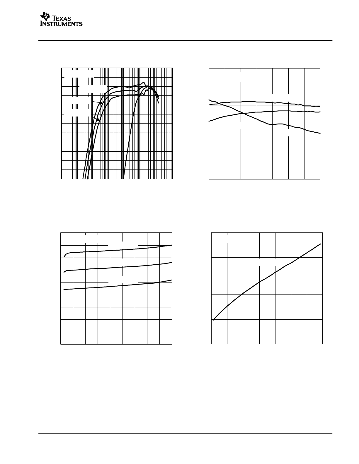
QUIESCENT CURRENT
vs
INPUT VOLTAGE
23
MODE = Low
21
TA = 85°C
EFFICIENCY
vs
INPUT VOLTAGE
100
VO = 1.8 V
MODE = Low
95
IL = 500 mA
90
85
IL = 1000 mA
Efficiency − %
80
75
70
2.5 3 3.5 4 4.5 5 5.5 6
VI − Input Voltage − V
IL = 1 mA
Figure 4
QUIESCENT CURRENT
vs
INPUT VOLTAGE
7.5
MODE = High
7
19
Aµ
17
15
13
11
Quisecent Current −
9
7
5
2.4 2.8 3.2 3.6 4 4.4 4.8 5.2 5.6 6
TA = 25°C
TA = −40°C
VI − Input Voltage − V
Figure 5
6.5
mA
6
5.5
5
4.5
Quisecent Current −
4
3.5
3
2.5 3 3.5 4 4.5 5 5.5 6
TA = 25°C
VI − Input Voltage − V
Figure 6
7
TPS62040
TPS62042, TPS62043
TPS62044, TPS62046
SLVS463B − JUNE 2003 − REVISED OCTOBER 2005
www.ti.com
SWITCHING FREQUENCY
vs
INPUT VOLTAGE
1.23
1.23
1.22
1.22
1.21
1.21
1.20
1.20
1.19
f − Switching Frequency − MHz
1.19
1.18
1.18
2.5 2.9 3.3 3.7 4.1 4.5 4.9 5.3 5.7 6
VI − Input Voltage − V
TA = 85°C
TA = −40°C
Figure 7
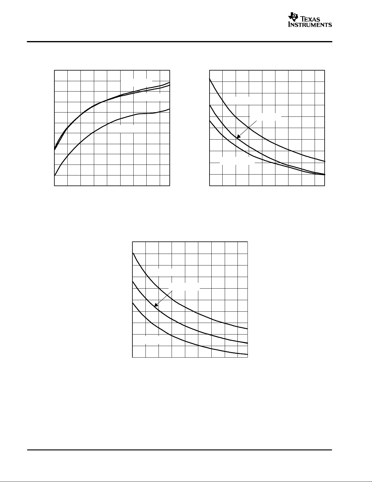
0.150
TA = 25°C
P−Channel r
N-CHANNEL RECTIFIER r
vs
INPUT VOLTAGE
P-CHANNEL r
DS(on)
vs
INPUT VOLTAGE
0.180
0.170
0.160
ΩDS(on) −
0.150
0.140
0.130
0.120
0.110
0.100
0.090
0.080
2.5 2.9 3.3 3.7 4.1 4.5 4.9 5.3 5.7 6
TA = 85°C
TA = 25°C
TA = −40°C
VI − Input Voltage − V
Figure 8
DS(on)
0.140
Ω
0.130
0.120
DS(on) −
0.110
0.100
0.090
0.080
N-Channel Rectifier r
0.070
0.060
0.050
TA = −40°C
2.5 2.9 3.3 3.7 4.1 4.5 4.9 5.3 5.7 6
TA = 85°C
TA = 25°C
VI − Input Voltage − V
Figure 9
8
www.ti.com
TPS62040
TPS62042, TPS62043
TPS62044, TPS62046
SLVS463B − JUNE 2003 − REVISED OCTOBER 2005
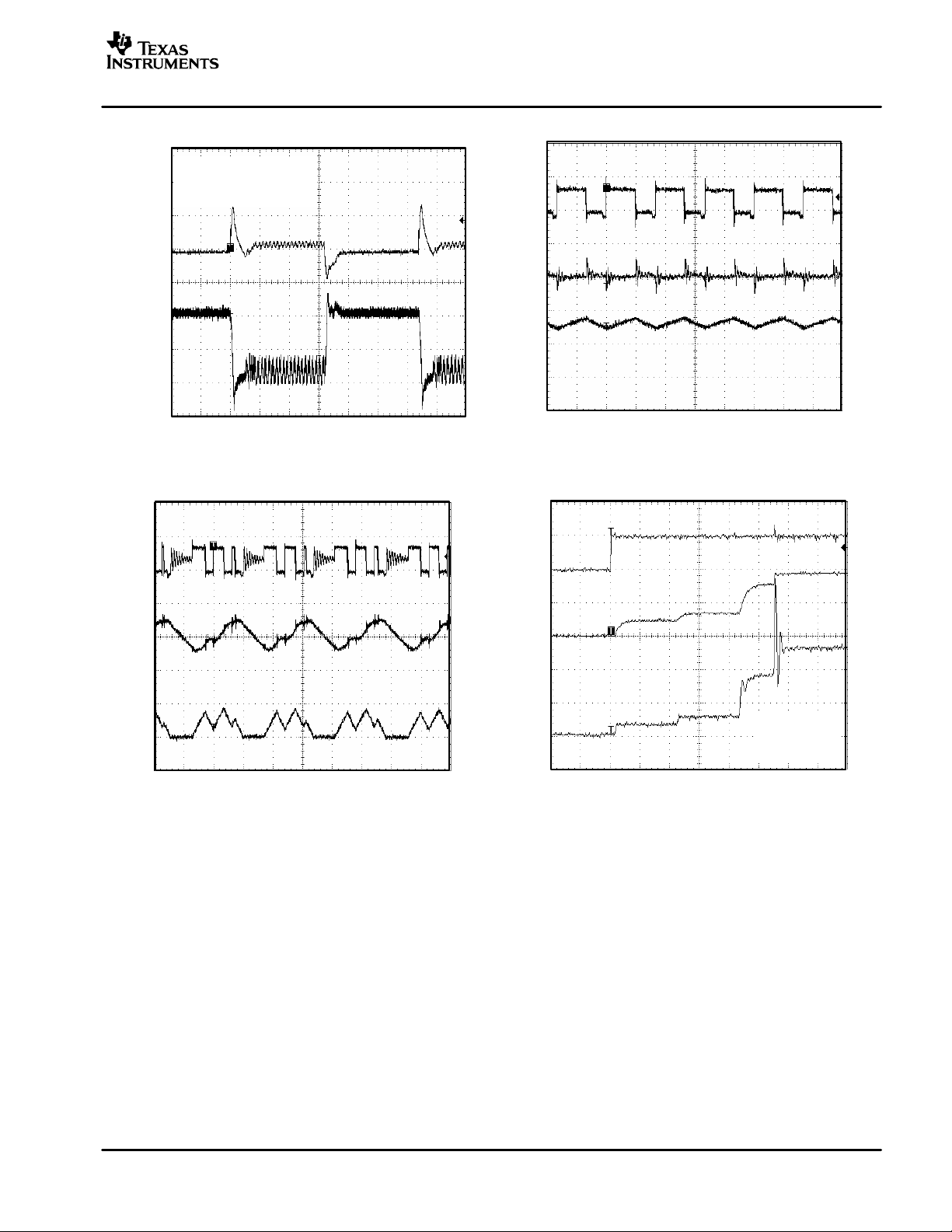
V
SW
VI = 3.6 V
VO = 1.8 V
PWM/PFM Operation
O
V
100 mV/div150mA to 1.15 A
O
I
5 V/div
LOAD TRANSIENT RESPONSE
50 µs/div
Figure 10
POWER SAVE MODE
SW
V
5 V/div
O
V
20 mV/div
L
I
500 mA/div
2 V/div
Enable
PWM OPERATION
500 ns/div
Figure 11
START-UP
O
V
20 mV/div
L
I
500 mA/div
2.5 µs/div
Figure 12
O
V
1 V/div
IN
I
200 mA/div
VI = 3.6 V
VO = 1.8 V
IO = 1.1 A
200 µs/div
Figure 13
9

TPS62040
TPS62042, TPS62043
TPS62044, TPS62046
SLVS463B − JUNE 2003 − REVISED OCTOBER 2005
DETAILED DESCRIPTION
OPERATION
The TPS6204x is a synchronous step-down converter operating with typically 1.25 MHz fixed frequency. At moderate
to heavy load currents, the device operates in pulse width modulation (PWM), and at light load currents, the device
enters power save mode operation using pulse frequency modulation (PFM). When operating in PWM mode, the
typical switching frequency is 1.25 MHz with a minimum switching frequency of 1 MHz. This makes the device
suitable for xDSL applications minimizing RF (radio frequency) interference.
During PWM operation the converter uses a unique fast response voltage mode controller scheme with input voltage
feed−forward to achieve good line and load regulation, allowing the use of small ceramic input and output capacitors.
At the beginning of each clock cycle initiated by the clock signal (S) the P-channel MOSFET switch turns on and the
inductor current ramps up until the comparator trips and the control logic turns off the switch. The current limit
comparator also turns off the switch in case the current limit of the P-channel switch is exceeded. After the dead time
preventing current shoot through, the N-channel MOSFET rectifier is turned on and the inductor current ramps down.
The next cycle is initiated by the clock signal, again turning off the N-channel rectifier and turning on the P-channel
switch.
www.ti.com
The Gm amplifier as well as the input voltage determines the rise time of the saw tooth generator, and therefore, any
change in input voltage or output voltage directly controls the duty cycle of the converter, giving a very good line and
load transient regulation.
POWER SAVE MODE OPERATION
As the load current decreases, the converter enters power save mode operation. During power save mode the
converter operates with reduced switching frequency in PFM mode and with a minimum quiescent current
maintaining high efficiency.
The converter monitors the average inductor current and the device enters power save mode when the average
inductor current is below the threshold. The transition point between PWM and power save mode is given by the
transition current with the following equation:
V
I
transition
During power save mode the output voltage is monitored with the comparator by the threshold’s comp low and comp
high. As the output voltage falls below the comp low threshold set to typically 0.8% above the nominal output voltage,
the P-channel switch turns on. The P-channel switch remains on until the transition current (1) is reached. Then the
N-channel switch turns on completing the first cycle. The converter continues to switch with its normal duty cycle
determined by the input and output voltage but with half the nominal switching frequency of 625-kHz typ. Thus the
output voltage rises and as soon as the output voltage reaches the comp high threshold of 1.6%, the converter stops
switching. Depending on the load current, the converter switches for a longer or shorter period of time in order to
deliver the energy to the output. If the load current increases and the output voltage can not be maintained with the
transition current , equation (1), the converter enters PWM again. See Figure 11 and Figure 12 under the typical
graphs section and Figure 14 for power save mode operation. Among other techniques this advanced power save
mode method allows high efficiency over the entire load current range and a small output ripple of typically 1% of
the nominal output voltage.
+
I
18.66 W
(1)
Setting the power save mode thresholds to typically 0.8% and 1.6% above the nominal output voltage at light load
current results in a dynamic voltage positioning achieving lower absolute voltage drops during heavy load transient
changes. This allows the converter to operate with small output capacitors like 22 µF and still having a low absolute
voltage drop during heavy load transient. Refer to Figure 14 as well for detailed operation of the power save mode.
10

www.ti.com
1.6%
TPS62040
TPS62042, TPS62043
TPS62044, TPS62046
SLVS463B − JUNE 2003 − REVISED OCTOBER 2005
PFM Mode at Light Load
Comp High
0.8%
V
O
PWM Mode at Medium to Full Load
Comp Low
Comp Low 2
Figure 14. Power Save Mode Thresholds and Dynamic Voltage Positioning
The converter enters the fixed frequency PWM mode as soon as the output voltage falls below the comp low 2
threshold.
DYNAMIC VOLTAGE POSITIONING
As described in the power save mode operation sections before and as detailed in Figure 14 the output voltage is
typically 0.8% (i.e., 1% on average) above the nominal output voltage at light load currents, as the device is in power
save mode. This gives additional headroom for the voltage drop during a load transient from light load to full load.
In the other direction during a load transient from full load to light load the voltage overshoot is also minimized by
turning on the N-Channel rectifier switch to pull the output voltage actively down.
MODE (AUTOMATIC PWM/PFM OPERATION AND FORCED PWM OPERATION)
Connecting the MODE pin to GND enables the automatic PWM and power save mode operation. The converter
operates in fixed frequency PWM mode at moderate to heavy loads and in the PFM mode during light loads,
maintaining high efficiency over a wide load current range.
Pulling the MODE pin high forces the converter to operate constantly in the PWM mode even at light load currents.
The advantage is the converter operates with a fixed switching frequency that allows simple filtering of the switching
frequency for noise sensitive applications. In this mode, the efficiency is lower compared to the power save mode
during light loads (see Figure 1 to Figure 3). For additional flexibility it is possible to switch from power save mode
to forced PWM mode during operation. This allows efficient power management by adjusting the operation of the
TPS6204x to the specific system requirements.
100% DUTY CYCLE LOW DROPOUT OPERATION
The TPS6204x offers a low input to output voltage difference while still maintaining regulation with the use of the 100%
duty cycle mode. In this mode, the P−Channel switch is constantly turned on. This is particularly useful in battery
powered applications to achieve longest operation time by taking full advantage of the whole battery voltage range.
i.e. The minimum input voltage to maintain regulation depends on the load current and output voltage and can be
calculated as:
VImin + VOmax ) IOmax ǒr
DS(on)
max ) R
with:
I
= maximum output current plus inductor ripple current
O(max)
r
max= maximum P-channel switch t
DS(on)
DS(on)
RL = DC resistance of the inductor
VOmax = nominal output voltage plus maximum output voltage tolerance
Ǔ
L
(2)
.
11

TPS62040
TPS62042, TPS62043
TPS62044, TPS62046
SLVS463B − JUNE 2003 − REVISED OCTOBER 2005
SOFTSTART
The TPS6204x series has an internal softstart circuit that limits the inrush current during start up. This prevents
possible voltage drops of the input voltage in case a battery or a high impedance power source is connected to the
input of the TPS6204x.
www.ti.com
The softstart is implemented with a digital circuit increasing the switch current in steps of typically I
and then the typical switch current limit 1.85 A as specified in the electrical parameter table. The start-up time mainly
depends on the output capacitor and load current, see Figure 13.
LIM
/8, I
LIM
/4, I
LIM
/2
SHORT-CIRCUIT PROTECTION
As soon as the output voltage falls below 50% of the nominal output voltage, the converter switching frequency as
well as the current limit is reduced to 50% of the nominal value. Since the short-circuit protection is enabled during
start-up, the device does not deliver more than half of its nominal current limit until the output voltage exceeds 50%
of the nominal output voltage. This needs to be considered in case a load acting as a current sink is connected to
the output of the converter.
THERMAL SHUTDOWN
As soon as the junction temperature of typically 150_C is exceeded the device goes into thermal shutdown. In this
mode, the P-Channel switch and N-Channel rectifier are turned off. The device continues its operation when the
junction temperature falls below typically 150°C again.
ENABLE
Pulling the EN low forces the part into shutdown mode, with a shutdown current of typically 0.1 µA. In this mode, the
P-Channel switch and N-Channel rectifier are turned off and the whole device is in shut down. If an output voltage
is present during shut down, which could be an external voltage source or super cap, the reverse leakage current
is specified under electrical parameter table. For proper operation the enable (EN) pin must be terminated and should
not be left floating.
Pulling EN high starts up the TPS6204x with the softstart as described under the section Softstart.
UNDERVOLTAGE LOCKOUT
The undervoltage lockout circuit prevents device misoperation at low input voltages. It prevents the converter from
turning on the switch or rectifier MOSFET with undefined conditions.
12

TPS62040
TPS62042, TPS62043
www.ti.com
SLVS463B − JUNE 2003 − REVISED OCTOBER 2005
APPLICATION INFORMATION
ADJUSTABLE OUTPUT VOLTAGE VERSION
When the adjustable output voltage version TPS62040 is used, the output voltage is set by the external resistor
divider. See Figure 15.
The output voltage is calculated as:
R1
VO+ 0.5 V ǒ1 )
R2
Ǔ
TPS62044, TPS62046
(3)
with R1 + R2 ≤ 1 MΩ and internal reference voltage V
typical = 0.5 V
ref
R1 + R2 should not be greater than 1 MΩ because of stability reasons. To keep the operating quiescent current to
a minimum, the feedback resistor divider should have high impedance with R1+R2≤1 MΩ. Due to this and the low
reference voltage of V
= 0.5 V, the noise on the feedback pin (FB) needs to be minimized. Using a capacitive divider
ref
C1 and C2 across the feedback resistors minimizes the noise at the feedback, without degrading the line or load
transient performance.
C1 and C2 should be selected as:
C1 +
2 p 10 kHz R1
1
(4)
with:
R1 = upper resistor of voltage divider
C1 = upper capacitor of voltage divider
For C1 a value should be chosen that comes closest to the calculated result.
R1
C2 +
R2
C1
(5)
with:
R2 = lower resistor of voltage divider
C2 = lower capacitor of voltage divider
For C2, the selected capacitor value should always be selected larger than the calculated result. For example, in
Figure 15 for C2 100 pF are selected for a calculated result of C2 = 88.42 pF.
If quiescent current is not a key design parameter C1 and C2 can be omitted, and a low impedance feedback divider
has to be used with R1 + R2 < 100 kΩ. This reduces the noise available on the feedback pin (FB) as well but increases
the overall quiescent current during operation. The higher the programmed output voltage the lower the feedback
impedance has to be for best operation when not using C1 and C2.
V
V
I
2.5 V to 6 V
C3
10 µF
TPS62040
2
VIN
3
VIN
1
EN
6
MODE
49
GND
SW
SW
FB
PGND
PGND
L1
10 µH
8
7
5
10
R1
470 kΩ
180 kΩ
R2
C1
33 pF
C2
100 pF
O
1.8 V / 1.2 A
C4
10 µF
Figure 15. Adjustable Output Voltage Version
13
TPS62040
TPS62042, TPS62043
TPS62044, TPS62046
SLVS463B − JUNE 2003 − REVISED OCTOBER 2005
Inductor Selection
The TPS6204x typically uses a 6.2-µH output inductor. Larger or smaller inductor values can be used to optimize
the performance of the device for specific operation conditions. The selected inductor has to be rated for its dc
resistance and saturation current. The dc resistance of the inductance directly influences the efficiency of the
converter. Therefore an inductor with the lowest dc resistance should be selected for highest efficiency.
Formula (7) calculates the maximum inductor current under static load conditions. The saturation current of the
inductor should be rated higher than the maximum inductor current as calculated with formula (7). This is needed
because during heavy load transient the inductor current rises above the value calculated under (7).
V
O
1–
V
DIL+ VO
ILmax + IOmax )
with
ƒ = Switching frequency (1.25 MHz typical)
L = Inductor value
∆IL= Peak-to-peak inductor ripple current
ILmax = Maximum inductor current
L ƒ
I
DI
L
2
www.ti.com
(6)
(7)
The highest inductor current occurs at maximum VI.
Open core inductors have a soft saturation characteristic and they can usually handle higher inductor currents versus
a comparable shielded inductor. A more conservative approach is to select the inductor current rating just for the
maximum switch current of 2.2 A for the TPS6204x. Keep in mind that the core material from inductor to inductor
differs and has an impact on the efficiency, especially at high switching frequencies. Refer to Table 1 and the typical
applications and inductors selection.
Table 1. Inductor Selection
INDUCTOR VALUE DIMENSIONS COMPONENT SUPPLIER
4.7 µH 5,0 mm × 5,0 mm × 3,0 mm Sumida CDRH4D28C-4.7
4.7 µH 5,2 mm × 5,2 mm × 2,5 mm Coiltronics SD25-4R7
5.3 µH 5,7 mm × 5,7 mm × 3,0 mm Sumida CDRH5D28-5R3
6.2 µH 5,7 mm × 5,7 mm × 3,0 mm Sumida CDRH5D28-6R2
6.0 µH 7,0 mm × 7,0 mm × 3,0 mm Sumida CDRH6D28-6R0
14

TPS62040
TPS62042, TPS62043
www.ti.com
SLVS463B − JUNE 2003 − REVISED OCTOBER 2005
Output Capacitor Selection
The advanced fast response voltage mode control scheme of the TPS6204x allows the use of small ceramic
capacitors with a typical value of 22 µF without having large output voltage under and overshoots during heavy load
transients. Ceramic capacitors having low ESR values have the lowest output voltage ripple and are recommended.
If required, tantalum capacitors may also be used. Refer to Table 2 for component selection.
If ceramic output capacitor are used, the capacitor RMS ripple current rating always meets the application
requirements. Just for completeness the RMS ripple current is calculated as:
V
O
1–
V
I
RMSCout
At nominal load current the device operates in PWM mode and the overall output voltage ripple is the sum of the
voltage spike caused by the output capacitor ESR plus the voltage ripple caused by charging and discharging the
output capacitor:
DVO+ VO
+ VO
V
1–
L ƒ
V
L ƒ
O
I
I
ǒ
1
8 CO ƒ
Ǹ
2 3
1
) ESR
Ǔ
TPS62044, TPS62046
(8)
(9)
Where the highest output voltage ripple occurs at the highest input voltage, VI.
At light load currents, the device operates in power save mode and the output voltage ripple is independent of the
output capacitor value. The output voltage ripple is set by the internal comparator thresholds. The typical output
voltage ripple is 1% of the nominal output voltage.
Input Capacitor Selection
Because of the nature of the buck converter having a pulsating input current, a low ESR input capacitor is required
for best input voltage filtering and minimizing the interference with other circuits caused by high input voltage spikes.
The input capacitor should have a minimum value of 22 µF. The input capacitor can be increased without any limit
for better input voltage filtering.
Table 2. Input and Output Capacitor Selection
CAPACITOR
VALUE
22 µF 1206 Taiyo Yuden JMK316BJ226ML Ceramic
22 µF 1210 Taiyo Yuden JMK325BJ226MM Ceramic
CASE SIZE COMPONENT SUPPLIER COMMENTS
15

TPS62040
TPS62042, TPS62043
TPS62044, TPS62046
SLVS463B − JUNE 2003 − REVISED OCTOBER 2005
Layout Considerations
For all switching power supplies, the layout is an important step in the design especially at high peak currents and
switching frequencies. If the layout is not carefully done, the regulator might show stability problems as well as EMI
problems. Therefore, use wide and short traces for the main current paths as indicated in bold in Figure 16. These
traces should be routed first. The input capacitor should be placed as close as possible to the IC pins as well as the
inductor and output capacitor. The feedback resistor network should be routed away from the inductor and switch
node to minimize noise and magnetic interference. To further minimize noise from coupling into the feedback network
and feedback pin, the ground plane or ground traces should be used for shielding. A common ground plane or a star
ground as shown below should be used. This becomes very important especially at high switching frequencies of
1.25 MHz.
The Switch Node Must Be
Kept as Small as Possible
www.ti.com
V
C3
22 µF
I
TPS6204x
2
VIN
3
VIN
1
EN
6
MODE
49
GND
SW
SW
FB
PGND
PGND
8
7
5
10
L1
10 µH
C2
22 µF
V
O
Figure 16. Layout Diagram
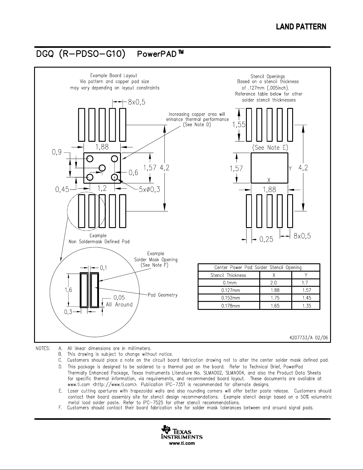
THERMAL INFORMATION
One of the most influential components on the thermal performance of a package is board design. In order to take
full advantage of the heat dissipating abilities of the PowerPADt packages, a board should be used that acts similar
to a heat sink and allows for the use of the exposed (and solderable), deep downset pad. For further information
please refer to Texas Instruments application note (SLMA002) PowerPAD Thermally Enhanced Package.
The PowerPADt of the 10-pin MSOP package has an area of 1,52 mm × 1,79 mm (± 0,05 mm) and must be soldered
to the PCB to lower the thermal resistance. Thermal vias to the next layer further reduce the thermal resistance.
16

www.ti.com
TYPICAL APPLICATIONS
TPS62040
TPS62042, TPS62043
TPS62044, TPS62046
SLVS463B − JUNE 2003 − REVISED OCTOBER 2005
V
O
3.3 V / 1.2 A
C2
22 µF
Components:
C1: Taiyo Yuden JMK316BJ226ML
C2: Taiyo Yuden JMK316BJ226ML
L1: Sumida CDRH5D28−6R2
V
I
Li-lon
22 µF
C1
2
3
1
6
4
TPS62046
VIN
VIN
EN
MODE
GND
SW
SW
FB
PGND
PGND
L1
6.2 µH
8
7
5
10
9
Figure 17. Li-Ion to 3.3 V/1.2 A Conversion
V
2.5 V to 6 V
Components:
C1: Taiyo Yuden JMK316BJ226ML
C2: Taiyo Yuden JMK316BJ226ML
L1: Sumida CDRH4D28C−4R7
C3
22 µF
V
I
TPS62040
2
VIN
3
VIN
1
EN
6
MODE
49
GND
SW
SW
FB
PGND
PGND
L1
4.7 µH
8
7
5
10
R1
470 kΩ
R2
180 kΩ
C1
33 pF
C2
100 pF
O
1.8 V / 1.2 A
C4
22 µF
Figure 18. Li-Ion to 1.8 V/1.2 A Conversion Using the Adjustable Output Voltage Version
17

PACKAGE OPTION ADDENDUM
www.ti.com
PACKAGING INFORMATION
Orderable Device Status
TPS62040DGQ ACTIVE MSOP-
TPS62040DGQG4 ACTIVE MSOP-
TPS62040DGQR ACTIVE MSOP-
TPS62040DGQRG4 ACTIVE MSOP-
TPS62040DRCR ACTIVE SON DRC 10 3000 Green (RoHS &
TPS62040DRCRG4 ACTIVE SON DRC 10 3000 Green (RoHS &
TPS62042DGQ ACTIVE MSOP-
TPS62042DGQG4 ACTIVE MSOP-
TPS62042DGQR ACTIVE MSOP-
TPS62042DGQRG4 ACTIVE MSOP-
TPS62042DRCR ACTIVE SON DRC 10 3000 Green (RoHS &
TPS62042DRCRG4 ACTIVE SON DRC 10 3000 Green (RoHS &
TPS62043DGQ ACTIVE MSOP-
TPS62043DGQG4 ACTIVE MSOP-
TPS62043DGQR ACTIVE MSOP-
TPS62043DGQRG4 ACTIVE MSOP-
TPS62043DRCR ACTIVE SON DRC 10 3000 Green (RoHS &
TPS62043DRCRG4 ACTIVE SON DRC 10 3000 Green (RoHS &
TPS62044DGQ ACTIVE MSOP-
TPS62044DGQG4 ACTIVE MSOP- DGQ 10 80 Green (RoHS & CU NIPDAU Level-1-260C-UNLIM
(1)
Package
Type
Power
PAD
Power
PAD
Power
PAD
Power
PAD
Power
PAD
Power
PAD
Power
PAD
Power
PAD
Power
PAD
Power
PAD
Power
PAD
Power
PAD
Power
PAD
Package
Drawing
DGQ 10 80 Green (RoHS &
DGQ 10 80 Green (RoHS &
DGQ 10 2500 Green (RoHS &
DGQ 10 2500 Green (RoHS &
DGQ 10 80 Green (RoHS &
DGQ 10 80 Green (RoHS &
DGQ 10 2500 Green (RoHS &
DGQ 10 2500 Green (RoHS &
DGQ 10 80 Green (RoHS &
DGQ 10 80 Green (RoHS &
DGQ 10 2500 Green (RoHS &
DGQ 10 2500 Green (RoHS &
DGQ 10 80 Green (RoHS &
Pins Package
Qty
Eco Plan
no Sb/Br)
no Sb/Br)
no Sb/Br)
no Sb/Br)
no Sb/Br)
no Sb/Br)
no Sb/Br)
no Sb/Br)
no Sb/Br)
no Sb/Br)
no Sb/Br)
no Sb/Br)
no Sb/Br)
no Sb/Br)
no Sb/Br)
no Sb/Br)
no Sb/Br)
no Sb/Br)
no Sb/Br)
(2)
Lead/Ball Finish MSL Peak Temp
CU NIPDAU Level-1-260C-UNLIM
CU NIPDAU Level-1-260C-UNLIM
CU NIPDAU Level-1-260C-UNLIM
CU NIPDAU Level-1-260C-UNLIM
CU NIPDAU Level-2-260C-1 YEAR
CU NIPDAU Level-2-260C-1 YEAR
CU NIPDAU Level-1-260C-UNLIM
CU NIPDAU Level-1-260C-UNLIM
CU NIPDAU Level-1-260C-UNLIM
CU NIPDAU Level-1-260C-UNLIM
CU NIPDAU Level-2-260C-1 YEAR
CU NIPDAU Level-2-260C-1 YEAR
CU NIPDAU Level-1-260C-UNLIM
CU NIPDAU Level-1-260C-UNLIM
CU NIPDAU Level-1-260C-UNLIM
CU NIPDAU Level-1-260C-UNLIM
CU NIPDAU Level-2-260C-1 YEAR
CU NIPDAU Level-2-260C-1 YEAR
CU NIPDAU Level-1-260C-UNLIM
5-Feb-2007
(3)
Addendum-Page 1

PACKAGE OPTION ADDENDUM
www.ti.com
Orderable Device Status
(1)
Package
Type
Power
Package
Drawing
Pins Package
Qty
Eco Plan
no Sb/Br)
(2)
Lead/Ball Finish MSL Peak Temp
5-Feb-2007
(3)
PAD
TPS62044DGQR ACTIVE MSOP-
Power
DGQ 10 2500 Green (RoHS &
no Sb/Br)
CU NIPDAU Level-1-260C-UNLIM
PAD
TPS62044DGQRG4 ACTIVE MSOP-
Power
DGQ 10 2500 Green (RoHS &
no Sb/Br)
CU NIPDAU Level-1-260C-UNLIM
PAD
TPS62044DRCR ACTIVE SON DRC 10 3000 Green (RoHS &
CU NIPDAU Level-2-260C-1 YEAR
no Sb/Br)
TPS62044DRCRG4 ACTIVE SON DRC 10 3000 Green (RoHS &
CU NIPDAU Level-2-260C-1 YEAR
no Sb/Br)
TPS62046DGQ ACTIVE MSOP-
Power
DGQ 10 80 Green (RoHS &
no Sb/Br)
CU NIPDAU Level-1-260C-UNLIM
PAD
TPS62046DGQG4 ACTIVE MSOP-
Power
DGQ 10 80 Green (RoHS &
no Sb/Br)
CU NIPDAU Level-1-260C-UNLIM
PAD
TPS62046DGQR ACTIVE MSOP-
Power
DGQ 10 2500 Green (RoHS &
no Sb/Br)
CU NIPDAU Level-1-260C-UNLIM
PAD
TPS62046DGQRG4 ACTIVE MSOP-
Power
DGQ 10 2500 Green (RoHS &
no Sb/Br)
CU NIPDAU Level-1-260C-UNLIM
PAD
TPS62046DRCR ACTIVE SON DRC 10 3000 Green (RoHS &
CU NIPDAU Level-2-260C-1 YEAR
no Sb/Br)
TPS62046DRCRG4 ACTIVE SON DRC 10 3000 Green (RoHS &
CU NIPDAU Level-2-260C-1 YEAR
no Sb/Br)
(1)
The marketing status values are defined as follows:
ACTIVE: Product device recommended for new designs.
LIFEBUY: TI has announced that the device will be discontinued, and a lifetime-buy period is in effect.
NRND: Not recommended for new designs. Device is in production to support existing customers, but TI does not recommend using this part in
a new design.
PREVIEW: Device has been announced but is not in production. Samples may or may not be available.
OBSOLETE: TI has discontinued the production of the device.
(2)
Eco Plan - The planned eco-friendly classification: Pb-Free (RoHS), Pb-Free (RoHS Exempt), or Green (RoHS & no Sb/Br) - please check
http://www.ti.com/productcontent for the latest availability information and additional product content details.
TBD: The Pb-Free/Green conversion plan has not been defined.
Pb-Free (RoHS): TI's terms "Lead-Free" or "Pb-Free" mean semiconductor products that are compatible with the current RoHS requirements
for all 6 substances, including the requirement that lead not exceed 0.1% by weight in homogeneous materials. Where designed to be soldered
at high temperatures, TI Pb-Free products are suitable for use in specified lead-free processes.
Pb-Free (RoHS Exempt): This component has a RoHS exemption for either 1) lead-based flip-chip solder bumps used between the die and
package, or 2) lead-based die adhesive used between the die and leadframe. The component is otherwise considered Pb-Free (RoHS
compatible) as defined above.
Green (RoHS & no Sb/Br): TI defines "Green" to mean Pb-Free (RoHS compatible), and free of Bromine (Br) and Antimony (Sb) based flame
retardants (Br or Sb do not exceed 0.1% by weight in homogeneous material)
(3)
MSL, Peak Temp. -- The Moisture Sensitivity Level rating according to the JEDEC industry standard classifications, and peak solder
temperature.
Important Information and Disclaimer:The information provided on this page represents TI's knowledge and belief as of the date that it is
provided. TI bases its knowledge and belief on information provided by third parties, and makes no representation or warranty as to the
accuracy of such information. Efforts are underway to better integrate information from third parties. TI has taken and continues to take
reasonable steps to provide representative and accurate information but may not have conducted destructive testing or chemical analysis on
incoming materials and chemicals. TI and TI suppliers consider certain information to be proprietary, and thus CAS numbers and other limited
Addendum-Page 2

PACKAGE OPTION ADDENDUM
www.ti.com
information may not be available for release.
In no event shall TI's liability arising out of such information exceed the total purchase price of the TI part(s) at issue in this document sold by TI
to Customer on an annual basis.
5-Feb-2007
Addendum-Page 3

PACKAGE MATERIALS INFORMATION
www.ti.com
TAPE AND REEL INFORMATION
11-Mar-2008
*All dimensions are nominal
Device Package
TPS62040DGQR MSOP-
Power
TPS62040DRCR SON DRC 10 3000 330.0 12.4 3.3 3.3 1.0 8.0 12.0 Q2
TPS62040DRCR SON DRC 10 3000 330.0 12.4 3.3 3.3 1.1 8.0 12.0 Q2
TPS62042DGQR MSOP-
Power
TPS62042DRCR SON DRC 10 3000 330.0 12.4 3.3 3.3 1.1 8.0 12.0 Q2
TPS62043DGQR MSOP-
Power
TPS62043DRCR SON DRC 10 3000 330.0 12.4 3.3 3.3 1.1 8.0 12.0 Q2
TPS62044DGQR MSOP-
Power
TPS62044DRCR SON DRC 10 3000 330.0 12.4 3.3 3.3 1.1 8.0 12.0 Q2
TPS62046DGQR MSOP-
Power
TPS62046DRCR SON DRC 10 3000 330.0 12.4 3.3 3.3 1.0 8.0 12.0 Q2
Type
PAD
PAD
PAD
PAD
PAD
Package
Drawing
Pins SPQ Reel
Diameter
(mm)
DGQ 10 2500 330.0 12.4 5.3 3.4 1.4 8.0 12.0 Q1
DGQ 10 2500 330.0 12.4 5.3 3.4 1.4 8.0 12.0 Q1
DGQ 10 2500 330.0 12.4 5.3 3.4 1.4 8.0 12.0 Q1
DGQ 10 2500 330.0 12.4 5.3 3.4 1.4 8.0 12.0 Q1
DGQ 10 2500 330.0 12.4 5.3 3.4 1.4 8.0 12.0 Q1
Reel
Width
W1 (mm)
A0 (mm) B0 (mm) K0 (mm) P1
(mm)W(mm)
Pin1
Quadrant
Pack Materials-Page 1

PACKAGE MATERIALS INFORMATION
www.ti.com
Device Package
TPS62046DRCR SON DRC 10 3000 330.0 12.4 3.3 3.3 1.1 8.0 12.0 Q2
Type
Package
Drawing
Pins SPQ Reel
Diameter
(mm)
Reel
Width
W1 (mm)
A0 (mm) B0 (mm) K0 (mm) P1
11-Mar-2008
(mm)W(mm)
Pin1
Quadrant
*All dimensions are nominal
Device Package Type Package Drawing Pins SPQ Length (mm) Width (mm) Height (mm)
TPS62040DGQR MSOP-PowerPAD DGQ 10 2500 346.0 346.0 29.0
TPS62040DRCR SON DRC 10 3000 370.0 355.0 55.0
TPS62040DRCR SON DRC 10 3000 346.0 346.0 29.0
TPS62042DGQR MSOP-PowerPAD DGQ 10 2500 346.0 346.0 29.0
TPS62042DRCR SON DRC 10 3000 346.0 346.0 29.0
TPS62043DGQR MSOP-PowerPAD DGQ 10 2500 346.0 346.0 29.0
TPS62043DRCR SON DRC 10 3000 346.0 346.0 29.0
TPS62044DGQR MSOP-PowerPAD DGQ 10 2500 346.0 346.0 29.0
TPS62044DRCR SON DRC 10 3000 346.0 346.0 29.0
TPS62046DGQR MSOP-PowerPAD DGQ 10 2500 346.0 346.0 29.0
TPS62046DRCR SON DRC 10 3000 370.0 355.0 55.0
TPS62046DRCR SON DRC 10 3000 346.0 346.0 29.0
Pack Materials-Page 2


IMPORTANT NOTICE
Texas Instruments Incorporated and its subsidiaries (TI) reserve the right to make corrections, modifications, enhancements, improvements,
and other changes to its products and services at any time and to discontinue any product or service without notice. Customers should
obtain the latest relevant information before placing orders and should verify that such information is current and complete. All products are
sold subject to TI’s terms and conditions of sale supplied at the time of order acknowledgment.
TI warrants performance of its hardware products to the specifications applicable at the time of sale in accordance with TI’s standard
warranty. Testing and other quality control techniques are used to the extent TI deems necessary to support this warranty. Except where
mandated by government requirements, testing of all parameters of each product is not necessarily performed.
TI assumes no liability for applications assistance or customer product design. Customers are responsible for their products and
applications using TI components. To minimize the risks associated with customer products and applications, customers should provide
adequate design and operating safeguards.
TI does not warrant or represent that any license, either express or implied, is granted under any TI patent right, copyright, mask work right,
or other TI intellectual property right relating to any combination, machine, or process in which TI products or services are used. Information
published by TI regarding third-party products or services does not constitute a license from TI to use such products or services or a
warranty or endorsement thereof. Use of such information may require a license from a third party under the patents or other intellectual
property of the third party, or a license from TI under the patents or other intellectual property of TI.
Reproduction of TI information in TI data books or data sheets is permissible only if reproduction is without alteration and is accompanied
by all associated warranties, conditions, limitations, and notices. Reproduction of this information with alteration is an unfair and deceptive
business practice. TI is not responsible or liable for such altered documentation. Information of third parties may be subject to additional
restrictions.
Resale of TI products or services with statements different from or beyond the parameters stated by TI for that product or service voids all
express and any implied warranties for the associated TI product or service and is an unfair and deceptive business practice. TI is not
responsible or liable for any such statements.
TI products are not authorized for use in safety-critical applications (such as life support) where a failure of the TI product would reasonably
be expected to cause severe personal injury or death, unless officers of the parties have executed an agreement specifically governing
such use. Buyers represent that they have all necessary expertise in the safety and regulatory ramifications of their applications, and
acknowledge and agree that they are solely responsible for all legal, regulatory and safety-related requirements concerning their products
and any use of TI products in such safety-critical applications, notwithstanding any applications-related information or support that may be
provided by TI. Further, Buyers must fully indemnify TI and its representatives against any damages arising out of the use of TI products in
such safety-critical applications.
TI products are neither designed nor intended for use in military/aerospace applications or environments unless the TI products are
specifically designated by TI as military-grade or "enhanced plastic." Only products designated by TI as military-grade meet military
specifications. Buyers acknowledge and agree that any such use of TI products which TI has not designated as military-grade is solely at
the Buyer's risk, and that they are solely responsible for compliance with all legal and regulatory requirements in connection with such use.
TI products are neither designed nor intended for use in automotive applications or environments unless the specific TI products are
designated by TI as compliant with ISO/TS 16949 requirements. Buyers acknowledge and agree that, if they use any non-designated
products in automotive applications, TI will not be responsible for any failure to meet such requirements.
Following are URLs where you can obtain information on other Texas Instruments products and application solutions:
Products Applications
Amplifiers amplifier.ti.com Audio www.ti.com/audio
Data Converters dataconverter.ti.com Automotive www.ti.com/automotive
DSP dsp.ti.com Broadband www.ti.com/broadband
Clocks and Timers www.ti.com/clocks Digital Control www.ti.com/digitalcontrol
Interface interface.ti.com Medical www.ti.com/medical
Logic logic.ti.com Military www.ti.com/military
Power Mgmt power.ti.com Optical Networking www.ti.com/opticalnetwork
Microcontrollers microcontroller.ti.com Security www.ti.com/security
RFID www.ti-rfid.com Telephony www.ti.com/telephony
RF/IF and ZigBee® Solutions www.ti.com/lprf Video & Imaging www.ti.com/video
Mailing Address: Texas Instruments, Post Office Box 655303, Dallas, Texas 75265
Copyright © 2008, Texas Instruments Incorporated
Wireless www.ti.com/wireless

 Loading...