

Page 1

TPS61177AEVM User Guide
User's Guide
Literature Number: SNVU490
OCTOBER 2015
Page 2

Contents
1 Introduction......................................................................................................................... 4
2 Set-Up ................................................................................................................................ 4
2.1 Input/Output Connector Description ................................................................................... 4
2.2 TPS61177AEVM Set-Up ................................................................................................ 6
2.2.1 Installation Guide for GUI Program (Windows7-Compatible)........................................... 6
2.3 Instructions fo Stand-Alone Evaluation .............................................................................. 18
2.4 Instructions for Evaluation With Software ........................................................................... 19
3 TPS61177AEVM Component Placement ................................................................................ 20
4 Schematic ......................................................................................................................... 22
5 TPS61177AEVM Bill of Materials .......................................................................................... 23
6 TPS61177A Usage and Programming.................................................................................... 24
6.1 In-Circuit Operation..................................................................................................... 24
6.2 ENABLE.................................................................................................................. 24
6.3 Boost Converter Configuration........................................................................................ 24
6.3.1 Setting the Boost Switching Frequency.................................................................. 24
6.3.2 Setting the Boost Voltage.................................................................................. 24
6.3.3 Setting the Boost Switch Slew Rate...................................................................... 24
6.4 LED Driver Configuration.............................................................................................. 24
6.4.1 Setting the Maximum LED Current ....................................................................... 24
6.4.2 PWM Output Frequency ................................................................................... 24
6.4.3 Dimming Mode Settings.................................................................................... 25
6.5 Support for Fault Conditions .......................................................................................... 25
6.5.1 Thermal Shutdown.......................................................................................... 25
6.5.2 Undervoltage Lockout ..................................................................................... 25
6.5.3 Undervoltage Lockout ..................................................................................... 25
6.5.4 Overvoltage Protection..................................................................................... 25
6.5.5 Undervoltage Lockout ..................................................................................... 25
6.6 ID Register............................................................................................................... 25
6.7 EEPROM Default Values .............................................................................................. 25
6.8 Instructions for Programming EEPROM............................................................................. 26
7 Related Documentation From Texas Instruments ................................................................... 26
2
Table of Contents SNVU490–OCTOBER 2015
Copyright © 2015, Texas Instruments Incorporated
Submit Documentation Feedback
Page 3

www.ti.com
1 TPS61177AEVM Evaluation Board ....................................................................................... 4
2 TPS61177AEVM With USB2Any Board Connected .................................................................... 6
3 TPS61177A GUI - First Page............................................................................................. 14
4 Option to Select Register Control ........................................................................................ 15
5 TPS61177A GUI - Register Control Page .............................................................................. 16
6 Default Jumper Configuration............................................................................................. 18
7 TPS61177A EVM Test Setup for Standalone Evaluation............................................................. 19
8 TPS61177A EVM Test Setup With USB2ANY Connected for Software Control .................................. 20
9 TPS61177AEVM Component Placement (Layout) .................................................................... 21
10 TPS61177AEVM Schematic.............................................................................................. 22
1 Device and Package Configurations ...................................................................................... 4
List of Figures
List of Tables
SNVU490–OCTOBER 2015 List of Figures
Submit Documentation Feedback
3
Copyright © 2015, Texas Instruments Incorporated
Page 4

Introduction
1 Introduction
The Texas Instruments TPS61177AEVM evaluation module (EVM) helps designers evaluate the operation
and performance of the TPS61177A High-Efficiency LED Backlight Driver. The device offers configurability
and can be set up to switch at 450 kHz, 600 kHz, 800 kHz, and 1.2 MHz.
The EVM contains one LED driver (see Table 1).
LED DRIVER IC PACKAGE
U1 TPS61177A VQFN
www.ti.com
Table 1. Device and Package Configurations
Figure 1. TPS61177AEVM Evaluation Board
2 Set-Up
This section describes the jumpers and connectors on the EVM, as well as how to properly connect, set
up, and use the TPS61177AEVM.
2.1 Input/Output Connector Description
J1 - Input: This header is the power input(VIN) terminal for the boost converter. The terminal provides a
power (VBAT) connection to allow the user to attach the EVM to a power supply.
J2 - Input: This header is the power input (GND) terminal for the boost converter. The terminal provides a
power ground(PGND) connection to allow the user to attach the EVM to a power supply.
J3 - Input: T his header is the power input terminal for the boost converter. The terminal provides a power
and power ground connection to allow the user to attach the EVM to a power supply using a 2-pin IDC
socket and also monitor VIN connected to J1.
J4 - Connector: This connector is for interfacing LED load board via ribbon cable or flying wires.
J5 - GND: This header connects to AGND to provide grounds for signal probing.
J6 - GND: This header connects to AGND to provide grounds for signal probing.
J7 - Input: This header connects to AGND to provide grounds for signal probing.
J8 - Connector: This connector is for interfacing with USB2ANY interface board for I2C communication
and control inputs such as PWM and EN signal.
4
List of Tables SNVU490–OCTOBER 2015
Copyright © 2015, Texas Instruments Incorporated
Submit Documentation Feedback
Page 5

www.ti.com
J9 - GND: This header connects to AGND to provide grounds for signal probing.
J10 - Connector: This connector is for interfacing LED load board(WLEDEVM-260) via 2 row ribbon
cable.
J17 - Connector: This connector is to use PWM signal from USB2ANY instead of VINor external one
chosen by JP9.
J18 - Connector: This connector is to use EN signal from USB2ANY instead of VINor external one
chosen by JP1.
JP1 - Jumper: This jumper is for selecting EN input state between high and low.
JP2 - Jumper: This jumper is for connecting VOUT to J4 and J10 for LED load connection.
JP3 to JP8 - Jumpers: These jumpers are for enabling or disabling LED channels.
JP9 - Jumper: This jumper is used to set PWM control. Connecting pin 1 and pin 2 will send high signal
to device and set full on. Connecting pin2 and pin3 will send low signal to device and set off.
JP10 - Jumper: This jumper is a small pad to place jumper resistor or current sensing resistor on VIN.
JP11 to JP16 - Jumpers: TThese jumpers are used to bypass 10-Ω series resistors to measure LED
string current.
JP17 - Jumper: This jumper is used to bypass series resistor on boost feedback (VLED) input.
JP18 - Jumper: This jumper is used to connect VIN to boost circuit or to bypass JP10.
TP1 - Test Point: This header is test point for VIN.
TP2 - Test Point: This header is test point for VINB.
TP3 - Test Point: This header is test point for VCC out.
TP4 - Test Point: This header is test point for boost switch node voltage.
TP5 - Test Point: This header is test point for REF.
TP6 - Test Point: This header is test point for VLED (boost feedback).
TP7 - Test Point: This header is test point for boost output voltage.
TP8 - Test Point: This header is test point for EN.
TP9 - Test Point: This header is test point for PWM input.
TP10 - Test Point: This header is test point for SCL (I2C clock).
TP11 - Test Point: This header is test point for SDA(I2C data).
TP12 - Test Point: This header is test point for CS1(LED driver out for channel 1).
TP13 - Test Point: This header is test point for CS6(LED driver out for channel 6).
Set-Up
SNVU490–OCTOBER 2015 List of Tables
Submit Documentation Feedback
5
Copyright © 2015, Texas Instruments Incorporated
Page 6

Set-Up
2.2 TPS61177AEVM Set-Up
www.ti.com
Figure 2. TPS61177AEVM With USB2Any Board Connected
External power must be provided to the board. A standard USB to mini USB cable must be connected to
the USB2ANY from a PC. The I2C-compatible interface program provides all of the controls that the
TPS61177A device requires.
For proper operation:
• - USB2ANY should be plugged into the PC before the interface program is opened.
• - Install and execute the GUI program – installation guide will be followed below.
• - Power the evaluation board
2.2.1 Installation Guide for GUI Program (Windows7-Compatible)
• Execute setup_TPS61177A_EVM.exe file : If it is compressed in zip file format, unzip first in any
location.
• Select “Run” though Windows security warning message appears
6
List of Tables SNVU490–OCTOBER 2015
Copyright © 2015, Texas Instruments Incorporated
Submit Documentation Feedback
Page 7

www.ti.com
• Click "Next" button.
Set-Up
• Check to accept the agreement and click “Next” button to proceed with installation.
SNVU490–OCTOBER 2015 List of Tables
Submit Documentation Feedback
7
Copyright © 2015, Texas Instruments Incorporated
Page 8

Set-Up
www.ti.com
• Click “Next” button. In default, program will be installed in C:\Program Files (x86)\Texas
Instruments\TPS61177A folder and Texas Instruments\TPS61177AEVM in start menu.
• Check to create a desktop icon for the program and click “Next” button.
8
List of Tables SNVU490–OCTOBER 2015
Copyright © 2015, Texas Instruments Incorporated
Submit Documentation Feedback
Page 9

www.ti.com
Set-Up
• Click “Install” button.
• Click “Finish” button to finish installation and launch the program.
SNVU490–OCTOBER 2015 List of Tables
Submit Documentation Feedback
9
Copyright © 2015, Texas Instruments Incorporated
Page 10

Set-Up
www.ti.com
• If firmware update of USB2ANY adaptor is needed this window will pop up.
• Depending on firmware versions in USB2ANY adaptors, this firmware uploader will appear, and then
follow the instruction on this window.
10
List of Tables SNVU490–OCTOBER 2015
Copyright © 2015, Texas Instruments Incorporated
Submit Documentation Feedback
Page 11
www.ti.com
Set-Up
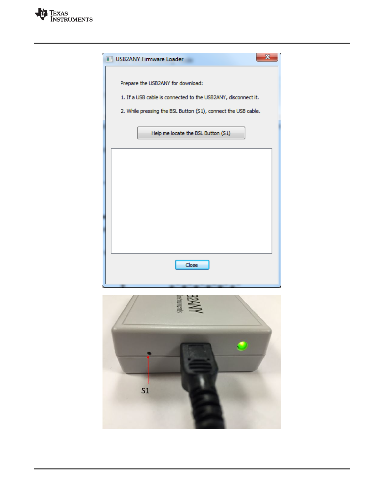
• After disconnecting USB cable and plugging it while pressing S1 button, this window will pop up and it
is ready to be updated. Press “Update Firmware” button.
SNVU490–OCTOBER 2015 List of Tables
Submit Documentation Feedback
11
Copyright © 2015, Texas Instruments Incorporated
Page 12

Set-Up
www.ti.com
• Update is finished.
12
List of Tables SNVU490–OCTOBER 2015
Copyright © 2015, Texas Instruments Incorporated
Submit Documentation Feedback
Page 13

www.ti.com
Set-Up
If firmware mismatch window appears after this process again, try to unplug USB cable from the box and
plug again.
The USB2ANY is recognized as an HID-compliant device in Windows Device Manager. After firmware
update is completed, successful communication with the board by the application is confirmed by the
"Connected" field at the bottom left corner with “Green” dot. This green dot becomes red when USB2ANY
is not detected by or disconnected from the PC and “Connected” will change to “Not connected”.
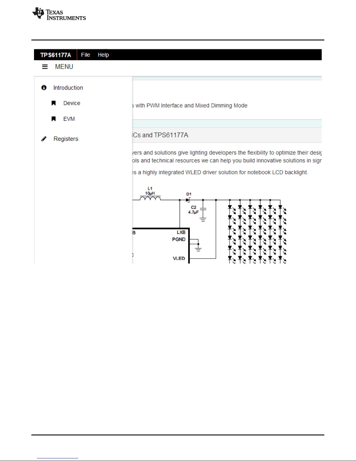
The first screen of the GUI will show the brief information and connecting diagram of the device (see
Figure 3).
SNVU490–OCTOBER 2015 List of Tables
Submit Documentation Feedback
13
Copyright © 2015, Texas Instruments Incorporated
Page 14

Set-Up
www.ti.com
Figure 3. TPS61177A GUI - First Page
In order to control registers of the device, click the icon on the upper left corner, and select
“Registers” page option.
14
List of Tables SNVU490–OCTOBER 2015
Copyright © 2015, Texas Instruments Incorporated
Submit Documentation Feedback
Page 15
www.ti.com
Set-Up
Figure 4. Option to Select Register Control
This is the register control window selected by the page option.
SNVU490–OCTOBER 2015 List of Tables
Submit Documentation Feedback
15
Copyright © 2015, Texas Instruments Incorporated
Page 16
Set-Up
www.ti.com
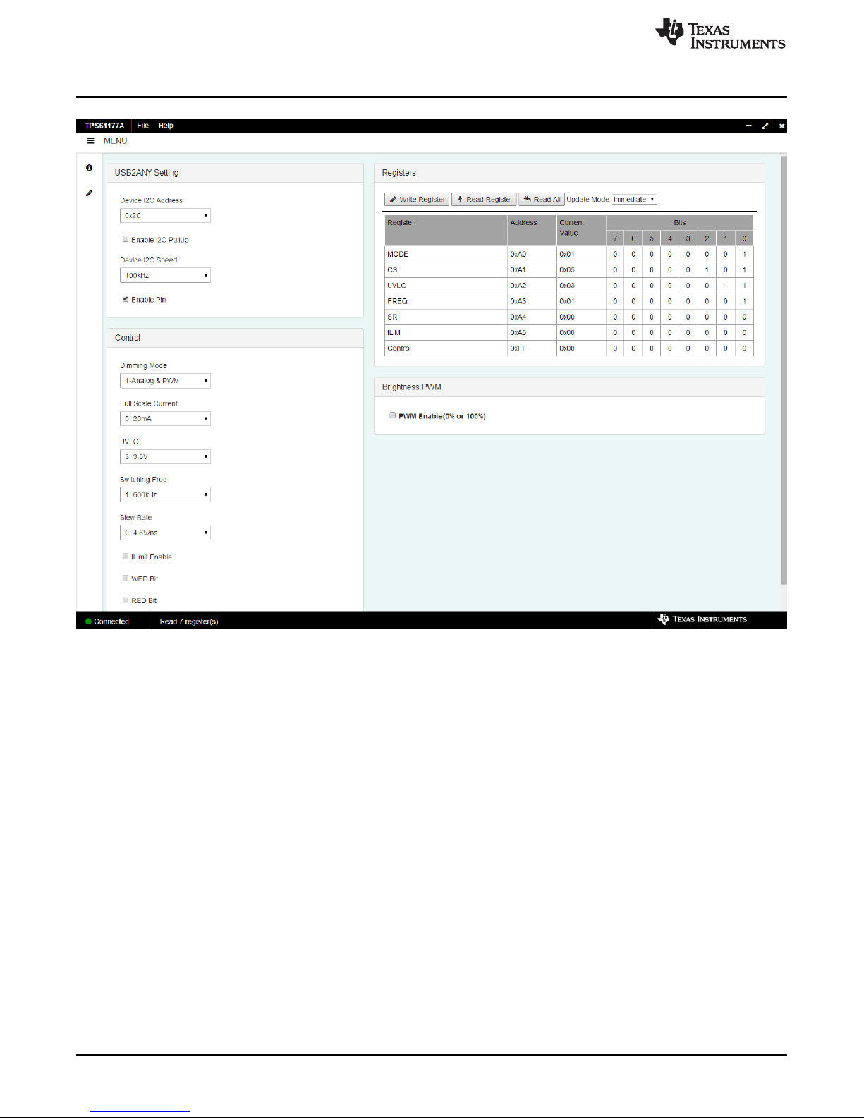
Figure 5. TPS61177A GUI - Register Control Page
The I2C-compatible device address is fixed at 0x58 (8-bit, 2Ch for 7-bit) in this program. The checkbox
“Enable I2C Pullup” is used to enable internal pullup (3.3 V) of USB2ANY when I2C pullup on
TPS61177AEVM is not available. I2C clock speed can be also selected from 1 0kHz to 400 kHz and
default speed is set to 100 kHz. EN signal from USB2ANY can be inserted by checking “Enable Pin”
checkbox. This is a useful control by GUI when Vin is not used as EN input by JP1(pin 1 and 2). J18
should be closed in this case. Register table on the right side can show the current values of the registers.
Press “Read All” button to read back all the registers and the values will be updated on this table. If any
register values need to changed, simply double click on the individual bit values to change it in this table
or press “Write Register” button to write all the registers at a time if “Deferred” is selected instead of
“Immediate” from dropdown box. “Brightness PWM” checkbox can be used to generate PWM input to the
device by USB2ANY and J17 should be closed for this control. Vin can be also used as PWM input(100%)
when JP9 (pins 1 and 2) is closed.
The minimum procedure for turning on the LEDs is as follows:
1. Connect the LED board (user-designed or WLEDEVM-260 from TI) to the TPS61177AEVM evaluation
board. Set jumpers for number of LEDs per string.
2. Connect external power and ground to the board.
• Suggest 12 V to VIN jack.
• Connect ground to GND jack.
3. Run “C:\Program Files (x86)\Texas Instruments\TPS61177A\nw.exe" or desktop icon
“TPS61177AEVM”.
16
List of Tables SNVU490–OCTOBER 2015
Copyright © 2015, Texas Instruments Incorporated
Submit Documentation Feedback
Page 17
www.ti.com
4. Turn on the external supplies
5. Check the "Enable Pin" box if EN signal from USB2ANY is used. EN will be tied to VIN by default
6. Change brightness with external PWM signal source on pin 2 of JP9 or GUI control (100% by enabling
The default dimming mode is analog and PWM mixed mode. This including other controls such as ILED
max, boost SW freq/slew rate, and UVLO can be also controlled through S/W GUI. See the TPS61177A
data sheet (SNVSA76) for detailed descriptions of the registers and their usage.
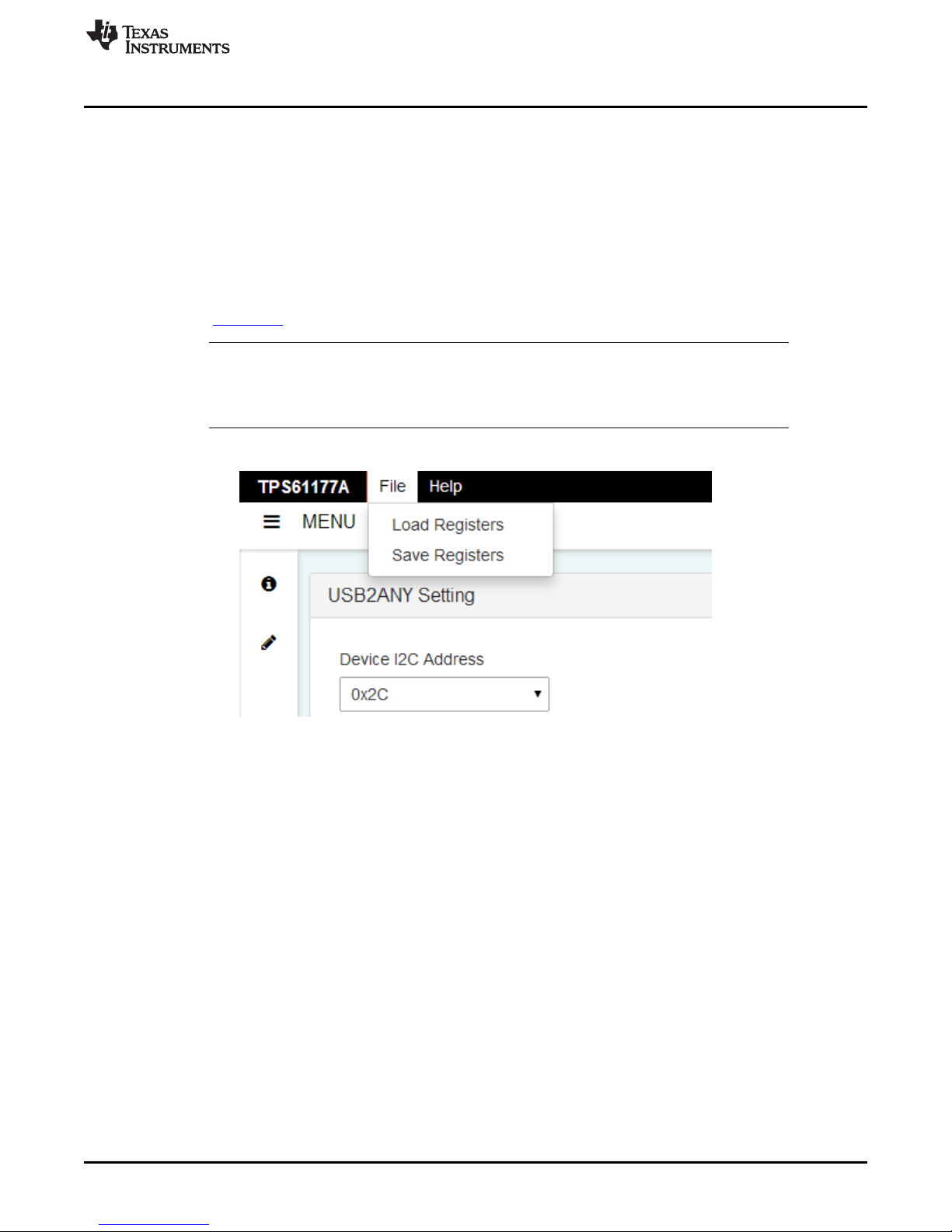
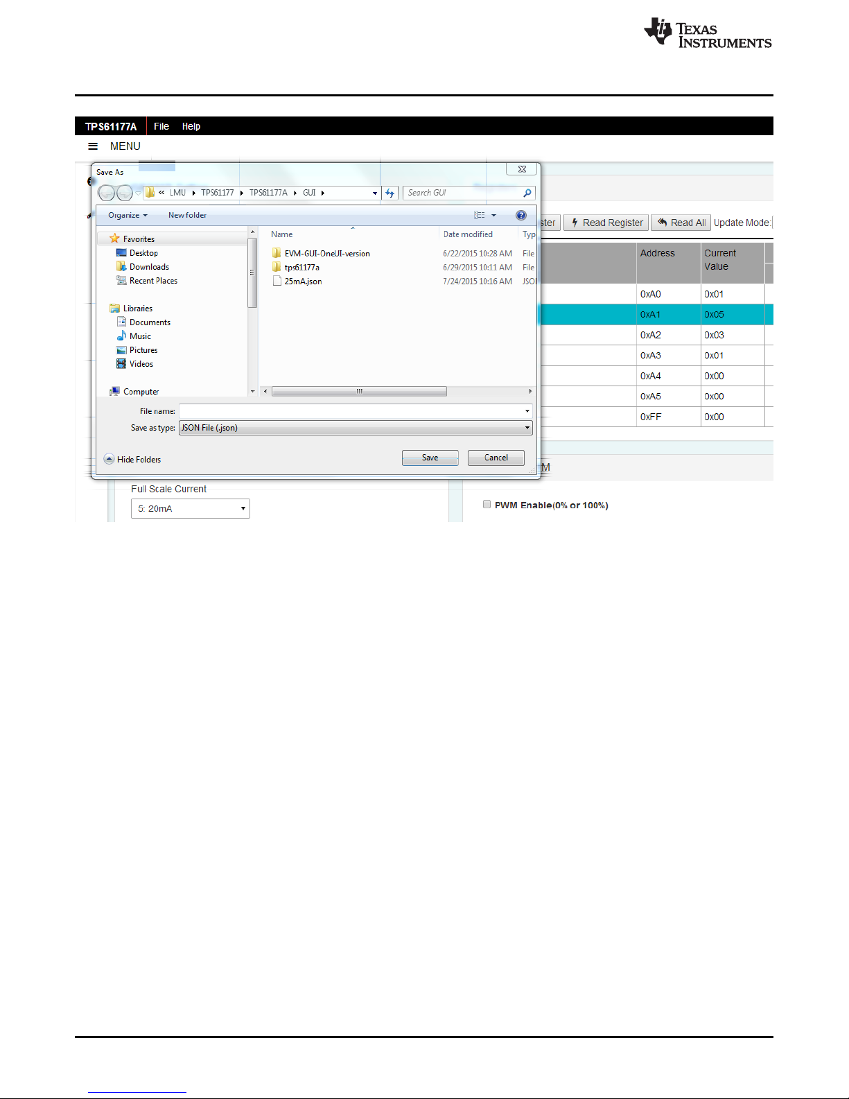
Register settings can be saved to “”*.json” file format by selecting “Save Registers” from file menu.
Set-Up
jumper connector setting and the jumper to connect EN to VIN should be removed when EN signal
from USB2ANY is used before VIN is enabled.
“PWM Enable” checkbox) with USB2ANY. PWM will be tied to VIN by default jumper connector setting
and the jumper (JP9) to connect PWM to VIN should be removed when PWM signal from USB2ANY is
used before VIN is enabled.
NOTE: Do not change the configuration of the device while the backlight is enabled. First disable the
backlight by making sure "Enable Backlight" is unchecked. Then adjust the configuration and
turn on the backlight. Changing the configuration while the backlight is on may produce
unexpected results.
Register settings saved as “*.json” file format can be opened and programmed automatically by selecting
“Load Register” from file menu.
SNVU490–OCTOBER 2015 List of Tables
Submit Documentation Feedback
17
Copyright © 2015, Texas Instruments Incorporated
Page 18
Set-Up
www.ti.com
Figure 6. Default Jumper Configuration
2.3 Instructions fo Stand-Alone Evaluation
The TPS61177A EVM can be used for TPS61177A standalone evaluation (without evaluation software) or
the evaluation with the software. Figure 7 shows the picture of the TPS61177A EVM board setup for the
standalone evaluation (LED load: WLEDEVM-260, not included in the kit).
18
List of Tables SNVU490–OCTOBER 2015
Copyright © 2015, Texas Instruments Incorporated
Submit Documentation Feedback
Page 19

www.ti.com
Set-Up
Figure 7. TPS61177A EVM Test Setup for Standalone Evaluation
The minimum procedure for turning on the LEDs with PWM only is as follows:
• Connect external power(VIN) and ground to the board.
• Recommend connecting 12 V to J1. (Any valid VIN2.7 V to 24 V : recommended boost conversion ratio
less than 10).
• Connect ground to J2.
• Connect an external PWM generator with levels 1.8 V or higher(but lower than VINB) with freq
between 0.1 kHz and 25 kHz to middle pin of JP9 or simply connect a jumper connector to JP9 to high
position(100% PWMB input)
• Check if EN input is at high position of JP1
• Turn on the external supplies.
2.4 Instructions for Evaluation With Software
The TPS61177A evaluation kit includes an I2C-compatible program and USB2ANY board that can help
exercise the part in a simple way. Contained in this document is a description of how to use the USB2ANY
board with the evaluation board and the interface software. Figure 8 shows the picture of the
TPS61177AEVM setup for the evaluation with software.
SNVU490–OCTOBER 2015 List of Tables
Submit Documentation Feedback
19
Copyright © 2015, Texas Instruments Incorporated
Page 20

TPS61177AEVM Component Placement
www.ti.com
Figure 8. TPS61177A EVM Test Setup With USB2ANY Connected for Software Control
The USB2ANY Board can be connected to the TPS61177AEVM via J8 connector. The USB2ANY Board
provides all of the control signals for the simple interface. Power to the part must be provided externally. A
standard USB cable must be connected to the USB2ANY board from a PC. The default jumper connection
of JP1 (EN) and JP9 (PWM) can be removed to use software control to enable and light up the board. J17
and J18 should be connected for software control of EN and PWM. PWM signal from USB2ANY is just on
(100%) /off (0%) signal for simple bring-up test for the board.
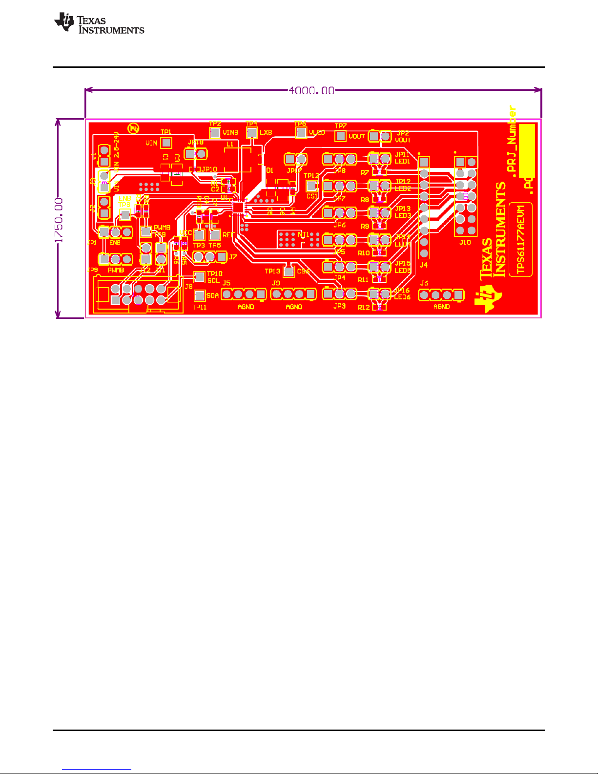
3 TPS61177AEVM Component Placement
Figure 9shows the top PCB layer of the TPS61177A EVM.
20
List of Tables SNVU490–OCTOBER 2015
Copyright © 2015, Texas Instruments Incorporated
Submit Documentation Feedback
Page 21
www.ti.com
TPS61177AEVM Component Placement
Figure 9. TPS61177AEVM Component Placement (Layout)
SNVU490–OCTOBER 2015 List of Tables
Submit Documentation Feedback
21
Copyright © 2015, Texas Instruments Incorporated
Page 22

Schematic
www.ti.com
4 Schematic
Figure 10. TPS61177AEVM Schematic
22
List of Tables SNVU490– OCTOBER 2015
Submit Documentation Feedback
Copyright © 2015, Texas Instruments Incorporated
Page 23

www.ti.com
5 TPS61177AEVM Bill of Materials
FOOTPRINT COMMENT PART NUMBER DESIGNATOR DESCRIPTION QTY
0805_HV C2012X5R1H475K125AB C2012X5R1H475K125AB C1, C5 CAP, CERM, 4.7 µF, 50 V, +/- 10%, X5R, 0801 2
0603 GMK107BJ105KA-T GMK107BJ105KA-T C2 CAP, CERM, 1 µF, 35 V, +/- 10%, X5R, 0608 1
1206 GMK316AB7106KL GMK316AB7106KL C3, C6 CAP, CERM, 10 µF, 35 V, +/- 10%, X7R, 1200 2
0603 GRM185R60J105KE26D GRM185R60J105KE26D C4 CAP, CERM, 1 µF, 6.3 V, +/- 10%, X5R, 0600 1
0603 GRM188R71E474KA12D GRM188R71E474KA12D C7 CAP, CERM, 0.47 µF, 25 V, +/- 10%, X7R, 0607 1
DO-220AA SS2P5-M3 SS2P5-M3 D1 Diode, Schottky, 50 V, 2 A, DO-220AA 1
WURTH_61300211121 VIN 2.5-24V TSW-102-07-G-S J1 Header, 100mil, 2x1, Gold, TH 1
WURTH_61300211121 GND TSW-102-07-G-S J2 Header, 100mil, 2x1, Gold, TH 1
WURTH_61300211121 VIN TSW-102-07-G-S J3 Header, 100mil, 2x1, Gold, TH 1
Samtec_TSW-109-07-G-S TSW-109-07-G-S TSW-109-07-G-S J4 Header, 100mil, 9x1, Gold, TH 1
WURTH_61300411121 AGND TSW-104-07-G-S J5, J6, J9 Header, 100mil, 4x1, Gold, TH 3
WURTH_61300311121 VAUX HTSW-103-07-G-S J7 Header, 100mil, 3x1, Gold, TH 1
CONN_2510-6002 N2510-6002-RB N2510-6002-RB J8 Header (shrouded), 100mil, 5x2, High- 1
TSW-107-07-G-D TSW-107-07-G-D TSW-107-07-G-D J10 Header, 100mil, 7x2, Gold, TH 1
WURTH_61300211121 TSW-102-07-G-S TSW-102-07-G-S J17, J18, JP17, JP18 Header, 100mil, 2x1, Gold, TH 4
WURTH_61300311121 ENB HTSW-103-07-G-S JP1 Header, 100mil, 3x1, Gold, TH 1
WURTH_61300211121 VOUT TSW-102-07-G-S JP2 Header,100mil, 2x1, Gold, TH 1
WURTH_61300311121 HTSW-103-07-G-S HTSW-103-07-G-S JP3, JP4, JP5, JP6, JP7, Header, 100mil, 3x1, Gold, TH 6
WURTH_61300311121 PWMB HTSW-103-07-G-S JP9 Header, 100mil, 3x1, Gold, TH 1
0402 MCR01MZPJ000 MCR01MZPJ000 JP10 RES, 0, 5%, 0.063 W, 0402 1
WURTH_61300211121 LED1 TSW-102-07-G-S JP11 Header, 100mil, 2x1, Gold, TH 1
WURTH_61300211121 LED2 TSW-102-07-G-S JP12 Header, 100mil, 2x1, Gold, TH 1
WURTH_61300211121 LED3 TSW-102-07-G-S JP13 Header, 100mil, 2x1, Gold, TH 1
WURTH_61300211121 LED4 TSW-102-07-G-S JP14 Header, 100mil, 2x1, Gold, TH 1
WURTH_61300211121 LED5 TSW-102-07-G-S JP15 Header, 100mil, 2x1, Gold, TH 1
WURTH_61300211121 LED6 TSW-102-07-G-S JP16 Header, 100mil, 2x1, Gold, TH 1
IHLP-2020BZ IHLP2020BZER100M01 IHLP2020BZER100M01 L1 Inductor, Shielded Drum Core, Powdered Iron,
NetTie_0603 Net-Tie Net-Tie NT1 Single point connection between nets. 1
0603 RC0603JR-070RL RC0603JR-070RL R1 RES, 0, 5%, 0.1 W, 0603 1
0603 CRCW060310K0JNEA CRCW060310K0JNEA R2, R3 RES, 10 k, 5%, 0.1 W, 0603 2
0603 RC0603FR-0749R9L RC0603FR-0749R9L R4 RES, 49.9, 1%, 0.1 W, 0603 1
0603 RC0603FR-072K2L RC0603FR-072K2L R5, R6 RES, 2.20 k, 1%, 0.1 W, 0603 2
0603 TNPW060310R0BEEA TNPW060310R0BEEA R7, R8, R9, R10, R11, R12 RES, 10.0, 0.1%, 0.1 W, 0603 6
0603 RC0603FR-0710RL RC0603FR-0710RL R13 RES, 10.0, 1%, 0.1 W, 0603 1
2SN-BK-G 2SN-BK-G 2SN-BK-G SH-JP1, SH-JP3, SH-JP4, Shunt, 2mm, Gold plated, Black 14
TSW-101-07-G-S VIN TSW-101-07-G-S TP1 Header, 100mil, 1pos, Gold, TH 1
TSW-101-07-G-S VINB TSW-101-07-G-S TP2 Header, 100mil, 1pos, Gold, TH 1
TSW-101-07-G-S VCC TSW-101-07-G-S TP3 Header,100mil, 1pos, Gold, TH 1
TSW-101-07-G-S LXB TSW-101-07-G-S TP4 Header, 100mil, 1pos, Gold, TH 1
TSW-101-07-G-S REF TSW-101-07-G-S TP5 Header, 100mil, 1pos, Gold, TH 1
TSW-101-07-G-S VLED TSW-101-07-G-S TP6 Header, 100mil, 1pos, Gold, TH 1
TSW-101-07-G-S VOUT TSW-101-07-G-S TP7 Header,100mil, 1pos, Gold, TH 1
TSW-101-07-G-S ENB TSW-101-07-G-S TP8 Header, 100mil, 1pos, Gold, TH 1
TSW-101-07-G-S PWMB TSW-101-07-G-S TP9 Header, 100mil, 1pos, Gold, TH 1
TSW-101-07-G-S SCL TSW-101-07-G-S TP10 Header, 100mil, 1pos, Gold, TH 1
TSW-101-07-G-S SDA TSW-101-07-G-S TP11 Header, 100mil, 1pos, Gold, TH 1
TSW-101-07-G-S CS1 TSW-101-07-G-S TP12 Header, 100mil, 1pos, Gold, TH 1
TSW-101-07-G-S CS6 TSW-101-07-G-S TP13 Header, 100mil, 1pos, Gold, TH 1
Label_650x200 Size: 0.65 in. x 0.20 in. THT-14-423-10 TPS61177AEVM Thermal Transfer Printable Labels, 0.650 inches 1
RGR0020A TPS61177ARGRR TPS61177ARGRR U1 WLED Driver for Notebooks with PWM Interface 1
JP8
SH-JP5, SH-JP6, SH-JP7,
SH-JP8, SH-JP9, SH-JP11,
SH-JP12, SH-JP13, SHJP14, SH-JP15, SH-JP16
TPS61177AEVM Bill of Materials
Temperature, Gold, TH
10 킜, 2.3 A, 0.184 Ω, SM
W x 0.200 inches H - 10,000 per roll
and Mixed Dimming Mode, RGR0020A
SNVU490–OCTOBER 2015 List of Tables
Submit Documentation Feedback
23
Copyright © 2015, Texas Instruments Incorporated
Page 24

TPS61177A Usage and Programming
6 TPS61177A Usage and Programming
The TPS61177A white LED driver can be programmed to support optimal application configuration for
boost and LED driver control by register control. The boost converter can operate at 4 switching
frequencies. Options can be set for slew rate control. The dimming can be done with a full PWM output,
linear current control, or an adaptive combination of the two for the both power savings and good dimming
quality. Shutdown for current limit can be also set to protect the circuit.
6.1 In-Circuit Operation
The TPS61177A white LED driver can be controlled during operation with I2C register accesses and PWM
input signal. I2C register access can be used for boost and LED driver control, and PWM input can be
used to adjust output dimming level of LED driver. Default EEPROM settings can be loaded to internal
registers at power up and these registers can be programmed for application conditions and burned in
EEPROM by simple I2C sequence.
6.2 ENABLE
The EN pin controls enabling and shutdown of the TPS61177A. A zero value on this pin holds the device
in shutdown with minimum current consumption. Register access is not available during shutdown. Boost
will not switch until valid PWM input higher than 0% is applied.
6.3 Boost Converter Configuration
The TPS61177A boost converter configuration is determined by the size of the LED array to be driven.
Additionally, component constraints will affect operating frequency selection. A calculation method is
described in datasheet for selecting the boost operating point and external components along with the
desired frequency of operation.
www.ti.com
6.3.1 Setting the Boost Switching Frequency
The desired frequency of operation is programmed in the FREQ bits of the A3h register. The default value
of FREQ bits is 01b setting 600kHz.
6.3.2 Setting the Boost Voltage
The boost voltage can be adaptively set by the TPS61177A to control the LED headroom in real time
which provides the most efficient operation. Boost maximum voltage is 39 V which can support up to 11 to
13 LEDs.
6.3.3 Setting the Boost Switch Slew Rate
The boost switch slew rate can be programmed in the SR bits of the A4h register. The slew rate control
can be used for optimization of EMI caused by boost or system efficiency
6.4 LED Driver Configuration
The LED driver can control the power to the LEDs using PWM dimming, pure current control, or an
adaptive combination of the two. See the Adaptive Dimming Control and Brightness Control sections of
the data sheet for descriptions.
6.4.1 Setting the Maximum LED Current
The desired maximum LED current is set in the CS bits of A1h. The CS value in A1h can be used for finer
adjustments of the maximum current. The default value of CS bits is 101b setting 20 mA.
6.4.2 PWM Output Frequency
PWM output freq on direct PWM mode and mixed dimming mode is determined by input PWM frequency.
24
List of Tables SNVU490–OCTOBER 2015
Copyright © 2015, Texas Instruments Incorporated
Submit Documentation Feedback
Page 25

www.ti.com
6.4.3 Dimming Mode Settings
The TPS61177A has 3 different types of LED dimming mode.
1. Direct PWM mode bypasses PWM input duty and freq to dimming output with same duty and freq. In
this case, large output load can switch potentially causing instability of the system such as power
fluctuation and audible noise. This mode is not recommended for generic applications.
2. Analog mode changes brightness value from PWM input into constant current value to dimming output.
System is more stable than direct PWM mode as there is no huge load transition condition.
3. Analog and PWM Mixed mode includes the advantages of both PWM and analog mode. Input PWM
duty is calculated to generate constant analog dimming output from 100% to 25% brightness. Analog
to PWM mode transition happens at 25% brightness. The duty of output PWM dimming signal will be
4x of input PWM duty below 25% as max current value will be only quarter of 100% brightness.
6.5 Support for Fault Conditions
6.5.1 Thermal Shutdown
The TPS61177A will shut down the LED outputs and the boost if the temperature exceeds 150°C. The
device will exit thermal shutdown when the temperature drops below 135°C.
6.5.2 Undervoltage Lockout
The TPS61177A will not start up until the VINB voltage is higher than the UVLO threshold which is preset
by EEPROM register data. During normal operation, if the VINB drops below UVLO with 200-mV
hysteresis, the TPS61177A immediately shuts down. There are 5 different UVLO levels from 2.25 V to 4
V.
TPS61177A Usage and Programming
6.5.3 Undervoltage Lockout
The TPS61177A will not start up until the VINB voltage is higher than the UVLO threshold which is preset
by EEPROM register data. During normal operation, if the VINB drops below UVLO with 200-mV
hysteresis, the TPS61177A immediately shuts down. There are 5 different UVLO levels from 2.25 V to 4
V.
6.5.4 Overvoltage Protection
The TPS61177A integrates output OVP which is fixed at 39.5 V typically. Once the VLED pin detects the
voltage higher than 39.5 V, the boost switching regulator stops switching until the voltage of VLED pin
drop below 39.5 V with 500-mV hysteresis.
6.5.5 Undervoltage Lockout
The TPS61177A has a pulse-by-pulse overcurrent limit of 1.8 A (minimum). The PWM switch turns off
when the inductor current reaches this current threshold. This protection can be disabled by EEPROM
register control (ILIM).
6.6 ID Register
The device slave register of TPS61177A is 58h in 8-bit (7bit slave address + R/W bit) or 2Ch in 7-bit
without R/W bit.
6.7 EEPROM Default Values
Refer to TPS61177A data sheet (SNVSA76) for detailed descriptions.
SNVU490–OCTOBER 2015 List of Tables
Submit Documentation Feedback
25
Copyright © 2015, Texas Instruments Incorporated
Page 26

TPS61177A Usage and Programming
6.8 Instructions for Programming EEPROM
Once TPS61177A register settings are finished to have optimal values for the application, internal
EEPROM values can be written with the programmed register settings, so they can be loaded to register
at next power up. Writing 80h to register addr FFh will write EEPROM with updated values or check “WED
bit” checkbox of the GUI.
7 Related Documentation From Texas Instruments
See the TPS61177A data sheet (SNVSA76) for more information.
www.ti.com
26
List of Tables SNVU490–OCTOBER 2015
Copyright © 2015, Texas Instruments Incorporated
Submit Documentation Feedback
Page 27

IMPORTANT NOTICE
Texas Instruments Incorporated and its subsidiaries (TI) reserve the right to make corrections, enhancements, improvements and other
changes to its semiconductor products and services per JESD46, latest issue, and to discontinue any product or service per JESD48, latest
issue. Buyers should obtain the latest relevant information before placing orders and should verify that such information is current and
complete. All semiconductor products (also referred to herein as “components”) are sold subject to TI’s terms and conditions of sale
supplied at the time of order acknowledgment.
TI warrants performance of its components to the specifications applicable at the time of sale, in accordance with the warranty in TI’s terms
and conditions of sale of semiconductor products. Testing and other quality control techniques are used to the extent TI deems necessary
to support this warranty. Except where mandated by applicable law, testing of all parameters of each component is not necessarily
performed.
TI assumes no liability for applications assistance or the design of Buyers’ products. Buyers are responsible for their products and
applications using TI components. To minimize the risks associated with Buyers’ products and applications, Buyers should provide
adequate design and operating safeguards.
TI does not warrant or represent that any license, either express or implied, is granted under any patent right, copyright, mask work right, or
other intellectual property right relating to any combination, machine, or process in which TI components or services are used. Information
published by TI regarding third-party products or services does not constitute a license to use such products or services or a warranty or
endorsement thereof. Use of such information may require a license from a third party under the patents or other intellectual property of the
third party, or a license from TI under the patents or other intellectual property of TI.
Reproduction of significant portions of TI information in TI data books or data sheets is permissible only if reproduction is without alteration
and is accompanied by all associated warranties, conditions, limitations, and notices. TI is not responsible or liable for such altered
documentation. Information of third parties may be subject to additional restrictions.
Resale of TI components or services with statements different from or beyond the parameters stated by TI for that component or service
voids all express and any implied warranties for the associated TI component or service and is an unfair and deceptive business practice.
TI is not responsible or liable for any such statements.
Buyer acknowledges and agrees that it is solely responsible for compliance with all legal, regulatory and safety-related requirements
concerning its products, and any use of TI components in its applications, notwithstanding any applications-related information or support
that may be provided by TI. Buyer represents and agrees that it has all the necessary expertise to create and implement safeguards which
anticipate dangerous consequences of failures, monitor failures and their consequences, lessen the likelihood of failures that might cause
harm and take appropriate remedial actions. Buyer will fully indemnify TI and its representatives against any damages arising out of the use
of any TI components in safety-critical applications.
In some cases, TI components may be promoted specifically to facilitate safety-related applications. With such components, TI’s goal is to
help enable customers to design and create their own end-product solutions that meet applicable functional safety standards and
requirements. Nonetheless, such components are subject to these terms.
No TI components are authorized for use in FDA Class III (or similar life-critical medical equipment) unless authorized officers of the parties
have executed a special agreement specifically governing such use.
Only those TI components which TI has specifically designated as military grade or “enhanced plastic” are designed and intended for use in
military/aerospace applications or environments. Buyer acknowledges and agrees that any military or aerospace use of TI components
which have not been so designated is solely at the Buyer's risk, and that Buyer is solely responsible for compliance with all legal and
regulatory requirements in connection with such use.
TI has specifically designated certain components as meeting ISO/TS16949 requirements, mainly for automotive use. In any case of use of
non-designated products, TI will not be responsible for any failure to meet ISO/TS16949.
Products Applications
Audio www.ti.com/audio Automotive and Transportation www.ti.com/automotive
Amplifiers amplifier.ti.com Communications and Telecom www.ti.com/communications
Data Converters dataconverter.ti.com Computers and Peripherals www.ti.com/computers
DLP® Products www.dlp.com Consumer Electronics www.ti.com/consumer-apps
DSP dsp.ti.com Energy and Lighting www.ti.com/energy
Clocks and Timers www.ti.com/clocks Industrial www.ti.com/industrial
Interface interface.ti.com Medical www.ti.com/medical
Logic logic.ti.com Security www.ti.com/security
Power Mgmt power.ti.com Space, Avionics and Defense www.ti.com/space-avionics-defense
Microcontrollers microcontroller.ti.com Video and Imaging www.ti.com/video
RFID www.ti-rfid.com
OMAP Applications Processors www.ti.com/omap TI E2E Community e2e.ti.com
Wireless Connectivity www.ti.com/wirelessconnectivity
Mailing Address: Texas Instruments, Post Office Box 655303, Dallas, Texas 75265
Copyright © 2015, Texas Instruments Incorporated
Page 28

Mouser Electronics
Authorized Distributor
Click to View Pricing, Inventory, Delivery & Lifecycle Information:
Texas Instruments:
TPS61177AEVM
 Loading...