

Texas Instruments TPS61040DBV, TPS61040DDC, TPS61040DRV, TPS61041DBV, TPS61041DRV Schematic [ru]
70
72
74
76
78
80
82
84
86
88
90
0.1 1 10 100
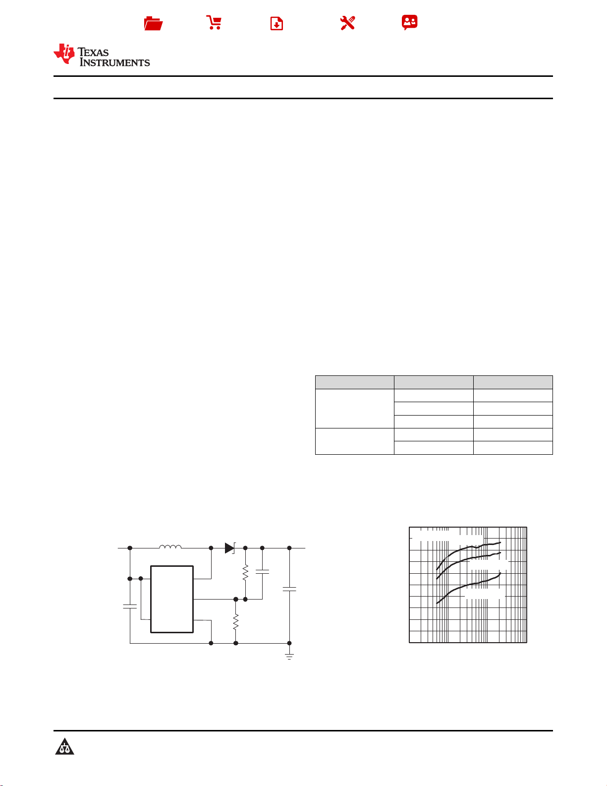
VI= 5 V
VI= 3.6 V
VI= 2.4 V
Efficiency vs Output Current
IO− Output Current − mA
Efficiency − %
V
IN
SW
FB
EN
GND
L1
10 mH
D1
R1
R2
C
FF
C
O
1 mF
V
OUT
VINto 28 V
V
IN
1.8 V to 6 V
C
IN
4.7 mF
5
4
2
3
1
VO= 18 V
Product
Folder
Sample &
Buy
Technical
Documents
Tools &
Software
Support &
Community
SLVS413H –OCTOBER 2002–REVISED OCTOBER 2015
TPS6104x Low-Power DC-DC Boost Converter in SOT-23 and WSON Packages
1 Features 3 Description
1
• 1.8-V to 6-V Input Voltage Range
• Adjustable Output Voltage Range up to 28 V
• 400-mA (TPS61040) and 250-mA (TPS61041)
Internal Switch Current
• Up to 1-MHz Switching Frequency
• 28-μA Typical No-Load Quiescent Current
• 1-μA Typical Shutdown Current
• Internal Soft Start
• Available in SOT23-5, TSOT23-5,
and 2-mm × 2-mm × 0.8-mm WSON Packages
2 Applications
• LCD Bias Supply
• White-LED Supply for LCD Backlights
• Digital Still Camera
• PDAs, Organizers, and Handheld PCs
• Cellular Phones
• Internet Audio Players
• Standard 3.3-V or 5-V to 12-V Conversion
The TPS6104x is a high-frequency boost converter
dedicated for small to medium LCD bias supply and
white LED backlight supplies. The device is ideal to
generate output voltages up to 28 V from a dual-cell
NiMH/NiCd or a single-cell Li-Ion battery. The part
can also be used to generate standard 3.3-V or 5-V
to 12-V power conversions.
The TPS6104x operates with a switching frequency
up to 1 MHz. This frequency allows the use of small
external components using ceramic as well as
tantalum output capacitors. Together with the thin
WSON package, the TPS6104x gives a very small
overall solution size. The TPS61040 device has an
internal 400-mA switch current limit, while the
TPS61041 device has a 250-mA switch current limit,
offering lower output voltage ripple and allows the
use of a smaller form factor inductor for lower power
applications. The low quiescent current (typically 28
μA) together with an optimized control scheme,
allows device operation at very high efficiencies over
the entire load current range.
Device Information
PART NUMBER PACKAGE BODY SIZE (NOM)
TPS61040 SOT (5) 2.90 mm ×1.60 mm
TPS61041
(1) For all available packages, see the orderable addendum at
the end of the datasheet.
TPS61040,TPS61041
(1)
SOT-23 (5) 2.90 mm × 1.60 mm
WSON (6) 2.00 mm × 2.00 mm
SOT-23 (5) 2.90 mm ×1.60 mm
WSON (6) 2.00 mm × 2.00 mm
4 Typical Application Schematic
1
An IMPORTANT NOTICE at the end of this data sheet addresses availability, warranty, changes, use in safety-critical applications,
intellectual property matters and other important disclaimers. PRODUCTION DATA.

TPS61040,TPS61041
SLVS413H –OCTOBER 2002–REVISED OCTOBER 2015
www.ti.com
Table of Contents
1 Features.................................................................. 1
2 Applications ........................................................... 1
3 Description ............................................................. 1
4 Typical Application Schematic............................. 1
5 Revision History..................................................... 2
6 Pin Configuration and Functions......................... 3
7 Specifications......................................................... 4
7.1 Absolute Maximum Ratings ...................................... 4
7.2 ESD Ratings.............................................................. 4
7.3 Recommended Operating Conditions....................... 4
7.4 Thermal Information.................................................. 4
7.5 Electrical Characteristics........................................... 5
7.6 Typical Characteristics.............................................. 6
8 Detailed Description .............................................. 9
8.1 Overview................................................................... 9
8.2 Functional Block Diagram ......................................... 9
8.3 Feature Description................................................... 9
8.4 Device Functional Modes........................................ 10
9 Application and Implementation ........................ 11
9.1 Application Information............................................ 11
9.2 Typical Application.................................................. 11
9.3 System Examples................................................... 16
10 Power Supply Recommendations ..................... 19
11 Layout................................................................... 19
11.1 Layout Guidelines................................................. 19
11.2 Layout Example.................................................... 19
12 Device and Documentation Support ................. 20
12.1 Third-Party Products Disclaimer ........................... 20
12.2 Related Links........................................................ 20
12.3 Community Resources.......................................... 20
12.4 Trademarks........................................................... 20
12.5 Electrostatic Discharge Caution............................ 20
12.6 Glossary................................................................ 20
13 Mechanical, Packaging, and Orderable
Information........................................................... 20
5 Revision History
Changes from Revision G (December 2014) to Revision H Page
• Added 500 µs/div label to X-axis of Figure 15. ................................................................................................................... 15
Changes from Revision F (December 2010) to Revision G Page
• Added ESD Ratings table, Feature Description section, Device Functional Modes, Application and Implementation
section, Power Supply Recommendations section, Layout section, Device and Documentation Support section, and
Mechanical, Packaging, and Orderable Information section.................................................................................................. 1
2 Submit Documentation Feedback Copyright © 2002–2015, Texas Instruments Incorporated
Product Folder Links: TPS61040 TPS61041
GND SW
V
IN
NC
EN FB
3
2
1
4
5
6
3
2
4
5
1
SW
GND
FB
V
IN
EN
www.ti.com
6 Pin Configuration and Functions
TPS61040,TPS61041
SLVS413H –OCTOBER 2002–REVISED OCTOBER 2015
DDC Package, DBV Package
5 Pins
Top View
DRV Package
6 Pins
Top View
Pin Functions
PIN
NAME DRV NO.
EN 4 3 I mode reducing the supply current to less than 1 μA. This pin should not be left floating and needs
FB 3 4 I
GND 2 1 – Ground
NC – 5 – No connection
SW 1 6 I
V
IN
DDC,
DBV NO.
5 2 I Supply voltage pin
I/O DESCRIPTION
This is the enable pin of the device. Pulling this pin to ground forces the device into shutdown
to be terminated.
This is the feedback pin of the device. Connect this pin to the external voltage divider to program
the desired output voltage.
Connect the inductor and the Schottky diode to this pin. This is the switch pin and is connected to
the drain of the internal power MOSFET.
Copyright © 2002–2015, Texas Instruments Incorporated Submit Documentation Feedback 3
Product Folder Links: TPS61040 TPS61041
TPS61040,TPS61041
SLVS413H –OCTOBER 2002–REVISED OCTOBER 2015
www.ti.com
7 Specifications
7.1 Absolute Maximum Ratings
over operating free-air temperature range (unless otherwise noted)
Supply voltages on pin V
Voltages on pins EN, FB
Switch voltage on pin SW
Operating junction temperature, T
Storage temperature, T
(1) Stresses beyond those listed under Absolute Maximum Ratings may cause permanent damage to the device. These are stress ratings
only, which do not imply functional operation of the device at these or any other conditions beyond those indicated under Recommended
Operating Conditions. Exposure to absolute-maximum-rated conditions for extended periods may affect device reliability.
(2) All voltage values are with respect to network ground terminal.
(2)
IN
(2)
(2)
J
stg
7.2 ESD Ratings
Human body model (HBM), per ANSI/ESDA/JEDEC JS-001
V
(ESD)
(1) JEDEC document JEP155 states that 500-V HBM allows safe manufacturing with a standard ESD control process. Manufacturing with
(2) JEDEC document JEP157 states that 250-V CDM allows safe manufacturing with a standard ESD control process. Manufacturing with
Electrostatic discharge V
Charged-device model (CDM), per JEDEC specification JESD22- ±750
(2)
C101
less than 500-V HBM is possible with the necessary precautions. Pins listed as ±XXX V may actually have higher performance.
less than 250-V CDM is possible with the necessary precautions. Pins listed as ±YYY V may actually have higher performance.
(1)
MIN MAX UNIT
–0.3 7 V
–0.3 VIN+ 0.3 V
30 30 V
–40 150 °C
–65 150 °C
VALUE UNIT
(1)
±2000
7.3 Recommended Operating Conditions
MIN NOM MAX UNIT
V
V
L Inductor
f Switching frequency
C
C
T
T
Input voltage range 1.8 6 V
IN
Output voltage range 28 V
OUT
IN
OUT
A
J
(1)
Input capacitor
Output capacitor
(1)
(1)
(1)
2.2 10 μH
1 μF
Operating ambient temperature –40 85 °C
Operating junction temperature –40 125 °C
1 MHz
4.7 μF
(1) See application section for further information.
7.4 Thermal Information
TPS61040 TPS61041
THERMAL METRIC
R
θJA
R
θJC(top)
R
θJB
ψ
JT
ψ
JB
R
θJC(bot)
Junction-to-ambient thermal resistance 205.2 214.7 83.0 205.2 83.0 °C/W
Junction-to-case (top) thermal resistance 118.3 38.5 57.1 118.3 57.1 °C/W
Junction-to-board thermal resistance 34.8 35.4 52.9 34.8 52.9 °C/W
Junction-to-top characterization parameter 12.2 0.4 2.4 12.2 2.4 °C/W
Junction-to-board characterization parameter 33.9 34.8 53.4 33.9 53.4 °C/W
Junction-to-case (bottom) thermal resistance — — 26.9 — 26.9 °C/W
(1) For more information about traditional and new thermal metrics, see the IC Package Thermal Metrics application report, SPRA953.
(1)
DBV DDC DRV DBV DRV UNIT
5 PINS 5 PINS 6 PINS 5 PINS 6 PINS
4 Submit Documentation Feedback Copyright © 2002–2015, Texas Instruments Incorporated
Product Folder Links: TPS61040 TPS61041
TPS61040,TPS61041
www.ti.com
SLVS413H –OCTOBER 2002–REVISED OCTOBER 2015
7.5 Electrical Characteristics
VIN= 2.4 V, EN = VIN, TA= –40°C to 85°C, typical values are at TA= 25°C (unless otherwise noted)
PARAMETER TEST CONDITIONS MIN TYP MAX UNIT
SUPPLY CURRENT
V
IN
I
Q
I
SD
V
UVLO
ENABLE
V
IH
V
IL
I
I
POWER SWITCH AND CURRENT LIMIT
Vsw Maximum switch voltage 30 V
t
off
t
on
R
DS(on)
R
DS(on)
I
LIM
I
LIM
OUTPUT
V
OUT
V
ref
I
FB
V
FB
(1) The line and load regulation depend on the external component selection. See the application section for further information.
Input voltage range 1.8 6 V
Operating quiescent current I
= 0 mA, not switching, VFB= 1.3 V 28 50 μA
OUT
Shutdown current EN = GND 0.1 1 μA
Undervoltage lockout threshold 1.5 1.7 V
EN high level input voltage 1.3 V
EN low level input voltage 0.4 V
EN input leakage current EN = GND or V
IN
0.1 1 μA
Minimum off time 250 400 550 ns
Maximum on time 4 6 7.5 μs
MOSFET on-resistance VIN= 2.4 V; ISW= 200 mA; TPS61040 600 1000 mΩ
MOSFET on-resistance VIN= 2.4 V; ISW= 200 mA; TPS61041 750 1250 mΩ
MOSFET leakage current VSW= 28 V 1 10 μA
MOSFET current limit TPS61040 350 400 450 mA
MOSFET current limit TPS61041 215 250 285 mA
Adjustable output voltage range V
IN
28 V
Internal voltage reference 1.233 V
Feedback input bias current VFB= 1.3 V 1 μA
Feedback trip point voltage 1.8 V ≤ VIN≤ 6 V 1.208 1.233 1.258 V
Line regulation
Load regulation
(1)
(1)
1.8 V ≤ VIN≤ 6 V; V
CFF= not connected
VIN= 2.4 V; V
OUT
= 18 V; I
OUT
= 18 V; 0 mA ≤ I
= 10 mA;
load
≤ 30 mA 0.15 %/mA
OUT
0.05 %/V
Copyright © 2002–2015, Texas Instruments Incorporated Submit Documentation Feedback 5
Product Folder Links: TPS61040 TPS61041

70
72
74
76
78
80
82
84
86
88
90
1 2 3 4 5 6
IO = 10 mA
IO = 5 mA
VI − Input Voltage − V
L = 10 µH
VO = 18 V
Efficiency − %
70
72
74
76
78
80
82
84
86
88
90
0.1 1 10
100
L = 10 µH
L = 3.3 µH
IL − Load Current − mA
VO = 18 V
Efficiency − %
Efficiency − %
70
72
74
76
78
80
82
84
86
88
90
0.1 1 10 100
VI = 5 V
VI = 3.6 V
VI = 2.4 V
IO − Output Current − mA
VO = 18 V
70
72
74
76
78
80
82
84
86
88
90
0.1 1 10 100
TPS61040
TPS61041
IL − Load Current − mA
L = 10 µH
VO = 18 V
Efficiency − %
TPS61040,TPS61041
SLVS413H –OCTOBER 2002–REVISED OCTOBER 2015
7.6 Typical Characteristics
η Efficiency
I
Q
V
FB
I
SW
I
CL
R
DS(on)
Quiescent current vs Input voltage and temperature Figure 5
Feedback voltage vs Temperature Figure 6
Switch current limit vs Temperature Figure 7
Switch current limit
R
DS(on)
Line transient response Figure 13
Load transient response Figure 14
Start-up behavior Figure 15
vs Load current Figure 2,
vs Input voltage Figure 4
vs Supply voltage, TPS61041 Figure 8
vs Supply voltage, TPS61040 Figure 9
vs Temperature Figure 10
vs Supply voltage Figure 11
www.ti.com
Table 1. Table of Graphs
FIGURE
Figure 1,
Figure 3
Figure 1. Efficiency vs Output Current Figure 2. Efficiency vs Load Current
6 Submit Documentation Feedback Copyright © 2002–2015, Texas Instruments Incorporated
Figure 3. Efficiency vs Load Current
Product Folder Links: TPS61040 TPS61041
Figure 4. Efficiency vs Input Voltage
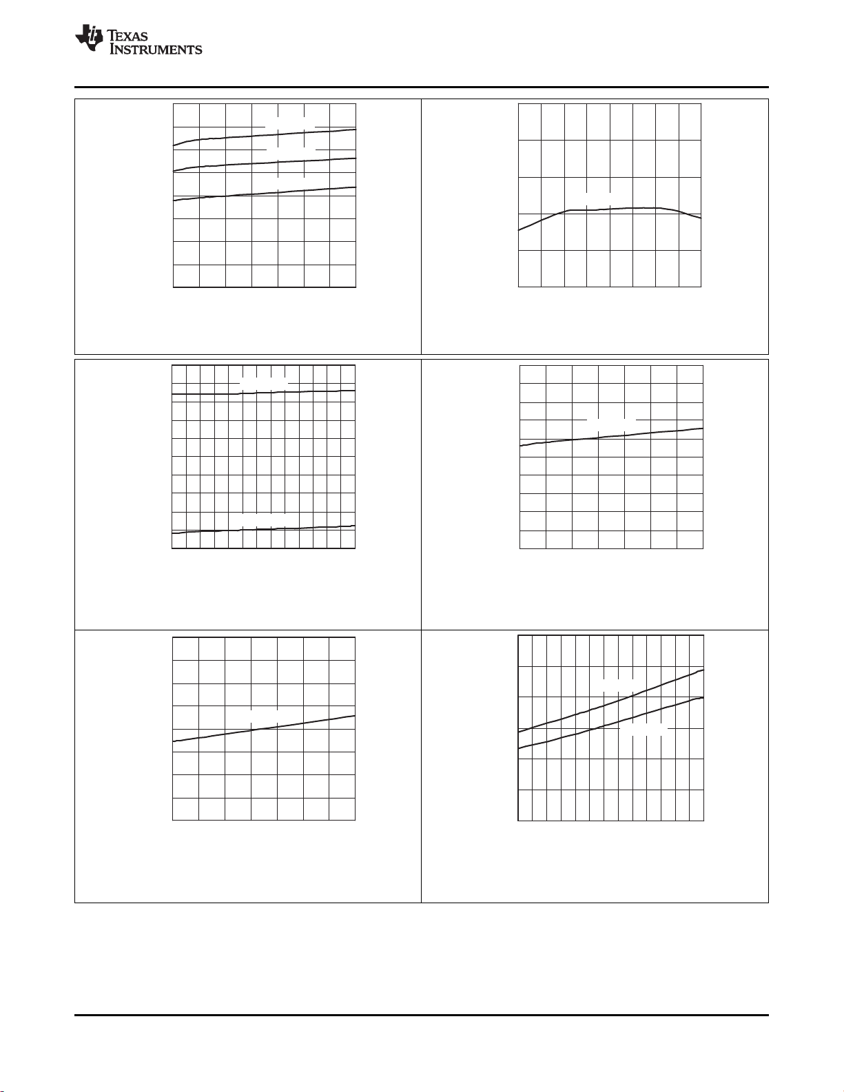
380
385
390
395
400
405
410
415
420
1.8 2.4 3 3.6 4.2 4.8 5.4 6
VCC − Supply Voltage − V
TA = 27°C
I
(CL)
− Current Limit − mA
0
200
400
600
800
1000
1200
−40−30 −20 −10 0 10 20 30 40 50 60 70 80 90
TA − Temperature − °C
TPS61041
TPS61040
r
DS(on)
− Static Drain-Source On-State Resistance − mΩ
230
250
270
290
310
330
350
370
390
410
430
−40−30−20 −10 0 10 20 30 40 50 60 70 80 90
TPS61040
TPS61041
TA − Temperature − °C
I
(SW)
− Switch Current Limit − mA
240
242
244
246
248
250
252
254
256
258
260
1.8 2.4 3 3.6 4.2 4.8 5.4 6
VCC − Supply Voltage − V
TA = 27°C
I
(CL)
− Current Limit − mA
0
5
10
15
20
25
30
35
40
1.8 2.4 3 3.6 4.2 4.8 5.4 6
VI − Input Voltage − V
TA = 85°C
TA = 27°C
TA = −40°C
Quiescent Current − µA
1.23
1.232
1.234
1.236
1.238
1.24
−40 −20 0 20 40 60 80 100 120
VCC = 2.4 V
TA − Temperature − °C
V
FB
− Feedback Voltage − V
www.ti.com
TPS61040,TPS61041
SLVS413H –OCTOBER 2002–REVISED OCTOBER 2015
Figure 5. TPS61040 Quiescent Current vs Input Voltage
Figure 6. Feedback Voltage vs Free-Air Temperature
Figure 7. TPS6104x Switch Current Limit vs Free-Air Figure 8. TPS61041 Current Limit vs Supply Voltage
Temperature
Copyright © 2002–2015, Texas Instruments Incorporated Submit Documentation Feedback 7
Figure 9. TPS61040 Current Limit vs Supply Voltage Figure 10. TPS6104x Static Drain-Source On-State
Resistance vs Free-Air Temperature
Product Folder Links: TPS61040 TPS61041
0
100
200
300
400
500
600
700
800
900
1000
1.8 2.4 3 3.6 4.2 4.8 5.4 6
VCC − Supply Voltage − V
TPS61041
TPS61040
r
DS(on)
− Static Drain-Source On-State Resistance − mΩ
TPS61040,TPS61041
SLVS413H –OCTOBER 2002–REVISED OCTOBER 2015
Figure 11. TPS6104x Static Drain-Source On-State Resistance vs Supply Voltage
www.ti.com
8 Submit Documentation Feedback Copyright © 2002–2015, Texas Instruments Incorporated
Product Folder Links: TPS61040 TPS61041
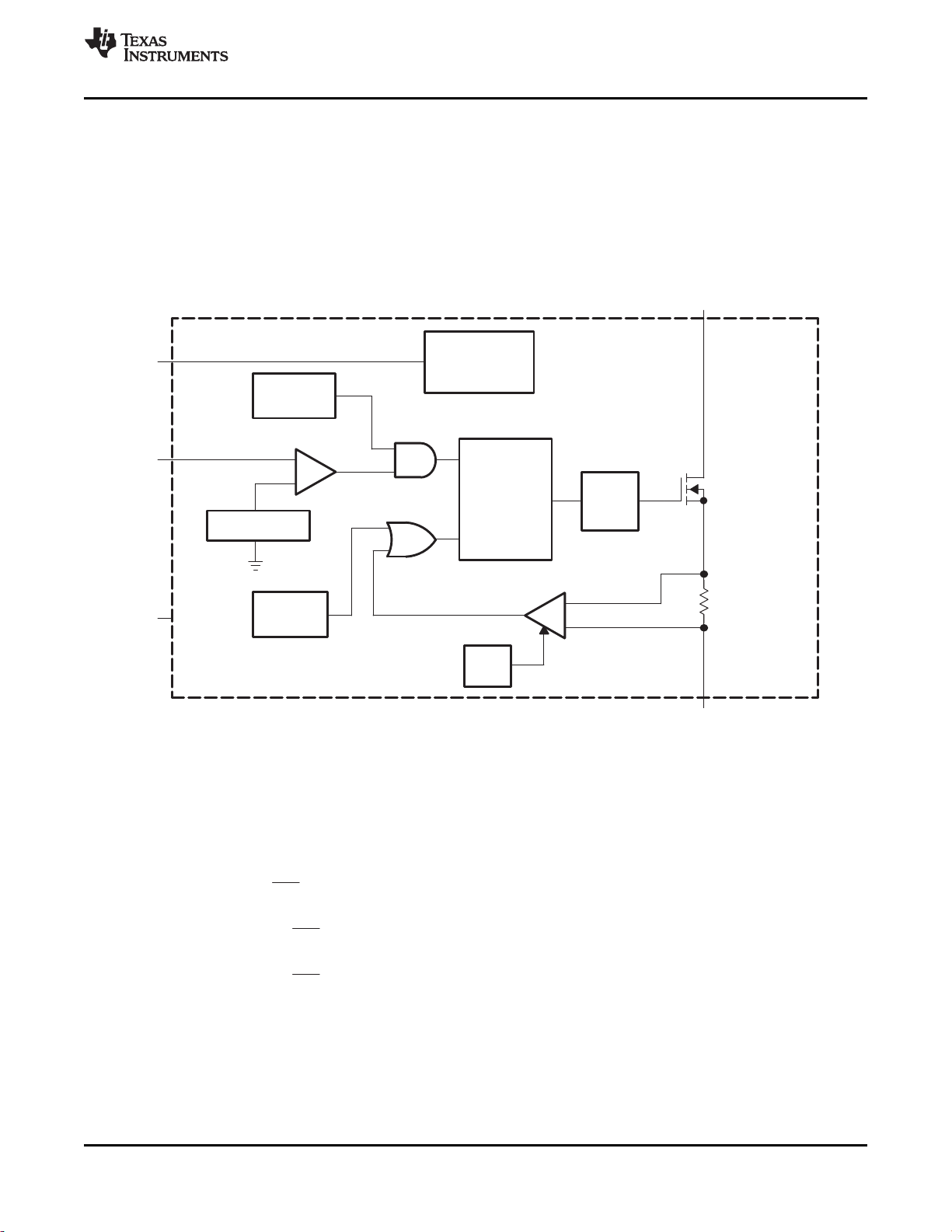
I
peak(typ)ILIM
V
IN
L
100 ns
I
peak(typ)
400 mA
V
IN
L
100 ns for the TPS61040
I
peak(typ)
250 mA
V
IN
L
100 ns for the TPS61041
=
=
=
+
+
+
×
×
×
+
+
-
RS Latch
Logic
S
R
Gate
Driver
_
Current Limit
Power MOSFET
N-Channel
R
SENSE
Soft
Start
6 µs Max
On Time
V
REF
= 1.233 V
Error Comparator
400 ns Min
Off Time
Under Voltage
Lockout
Bias Supply
VIN
FB
EN
GND
SW
TPS61040,TPS61041
www.ti.com
SLVS413H –OCTOBER 2002–REVISED OCTOBER 2015
8 Detailed Description
8.1 Overview
The TPS6104x is a high-frequency boost converter dedicated for small to medium LCD bias supply and white
LED backlight supplies. The device is ideal to generate output voltages up to 28 V from a dual-cell NiMH/NiCd or
a single cell device Li-Ion battery.
8.2 Functional Block Diagram
8.3 Feature Description
8.3.1 Peak Current Control
The internal switch turns on until the inductor current reaches the typical dc current limit (I
(TPS61040) or 250 mA (TPS61041). Due to the internal propagation delay of typical 100 ns, the actual current
exceeds the dc current limit threshold by a small amount. The typical peak current limit can be calculated:
The higher the input voltage and the lower the inductor value, the greater the peak.
By selecting the TPS6104x, it is possible to tailor the design to the specific application current limit requirements.
A lower current limit supports applications requiring lower output power and allows the use of an inductor with a
lower current rating and a smaller form factor. A lower current limit usually has a lower output voltage ripple as
well.
Copyright © 2002–2015, Texas Instruments Incorporated Submit Documentation Feedback 9
Product Folder Links: TPS61040 TPS61041
) of 400 mA
LIM
(1)

I
LIM
2
I
LIM
4
TPS61040,TPS61041
SLVS413H –OCTOBER 2002–REVISED OCTOBER 2015
www.ti.com
Feature Description (continued)
8.3.2 Soft Start
All inductive step-up converters exhibit high inrush current during start-up if no special precaution is made. This
can cause voltage drops at the input rail during start up and may result in an unwanted or early system shut
down.
The TPS6104x limits this inrush current by increasing the current limit in two steps starting from for 256
cycles to for the next 256 cycles, and then full current limit (see Figure 15).
8.3.3 Enable
Pulling the enable (EN) to ground shuts down the device reducing the shutdown current to 1 μA (typical).
Because there is a conductive path from the input to the output through the inductor and Schottky diode, the
output voltage is equal to the input voltage during shutdown. The enable pin needs to be terminated and should
not be left floating. Using a small external transistor disconnects the input from the output during shutdown as
shown in Figure 17.
8.3.4 Undervoltage Lockout
An undervoltage lockout prevents misoperation of the device at input voltages below typical 1.5 V. When the
input voltage is below the undervoltage threshold, the main switch is turned off.
8.3.5 Thermal Shutdown
An internal thermal shutdown is implemented and turns off the internal MOSFETs when the typical junction
temperature of 168°C is exceeded. The thermal shutdown has a hysteresis of typically 25°C. This data is based
on statistical means and is not tested during the regular mass production of the IC.
8.4 Device Functional Modes
8.4.1 Operation
The TPS6104x operates with an input voltage range of 1.8 V to 6 V and can generate output voltages up to 28
V. The device operates in a pulse-frequency-modulation (PFM) scheme with constant peak current control. This
control scheme maintains high efficiency over the entire load current range, and with a switching frequency up to
1 MHz, the device enables the use of very small external components.
The converter monitors the output voltage, and as soon as the feedback voltage falls below the reference voltage
of typically 1.233 V, the internal switch turns on and the current ramps up. The switch turns off as soon as the
inductor current reaches the internally set peak current of typically 400 mA (TPS61040) or 250 mA (TPS61041).
See Peak Current Control for more information. The second criteria that turns off the switch is the maximum ontime of 6 μs (typical). This is just to limit the maximum on-time of the converter to cover for extreme conditions.
As the switch is turned off the external Schottky diode is forward biased delivering the current to the output. The
switch remains off for a minimum of 400 ns (typical), or until the feedback voltage drops below the reference
voltage again. Using this PFM peak current control scheme the converter operates in discontinuous conduction
mode (DCM) where the switching frequency depends on the output current, which results in very high efficiency
over the entire load current range. This regulation scheme is inherently stable, allowing a wider selection range
for the inductor and output capacitor.
10 Submit Documentation Feedback Copyright © 2002–2015, Texas Instruments Incorporated
Product Folder Links: TPS61040 TPS61041

V
IN
SW
FB
EN
GND
L1
10 µH
D1
R1
2.2 MW
R2
160 kW
C
FF
22 pF
C2
1 µF
V
OUT
18 V
V
IN
1.8 V to 6 V
C1
4.7 µF
L1: Sumida CR32-100
D1: Motorola MBR0530
C1: Tayo Yuden JMK212BY475MG
C2: Tayo Yuden TMK316BJ105KL
TPS61040
TPS61040,TPS61041
www.ti.com
SLVS413H –OCTOBER 2002–REVISED OCTOBER 2015
9 Application and Implementation
NOTE
Information in the following applications sections is not part of the TI component
specification, and TI does not warrant its accuracy or completeness. TI’s customers are
responsible for determining suitability of components for their purposes. Customers should
validate and test their design implementation to confirm system functionality.
9.1 Application Information
The TPS6104x is designed for output voltages up to 28 V with an input voltage range of 1.8 V to 6 V and a
switch peak current limit of 400 mA (250 mA for the TPS61041). The device operates in a pulse-frequencymodulation (PFM) scheme with constant peak current control. This control scheme maintains high efficiency over
the entire load current range, and with a switching frequency up to 1 MHz, the device enables the use of very
small external components. The following section provides a step-by-step design approach for configuring the
TPS61040 as a voltage regulating boost converter for LCD bias power supply, as shown in Figure 12.
9.2 Typical Application
The following section provides a step-by-step design approach for configuring the TPS611040 as a voltage
regulating boost converter for LCD bias supply, as shown in Figure 12.
Figure 12. LCD Bias Supply
9.2.1 Design Requirements
Table 2. Design Parameters
DESIGN PARAMETER EXAMPLE VALUE
Input Voltage 1.8 V to 6 V
Output Voltage 18 V
Output Current 10 mA
9.2.2 Detailed Design Procedure
9.2.2.1 Inductor Selection, Maximum Load Current
Because the PFM peak current control scheme is inherently stable, the inductor value does not affect the stability
of the regulator. The selection of the inductor together with the nominal load current, input and output voltage of
the application determines the switching frequency of the converter. Depending on the application, inductor
values from 2.2 μH to 47 μH are recommended. The maximum inductor value is determined by the maximum on
time of the switch, typically 6 μs. The peak current limit of 400 mA/250 mA (typically) should be reached within
this 6-μs period for proper operation.
Copyright © 2002–2015, Texas Instruments Incorporated Submit Documentation Feedback 11
Product Folder Links: TPS61040 TPS61041

I
load max
+ h
I
2
P
L fS
max
2 (V
OUT
* V
IN)
fS I
load
2 I
load
(V
OUT
V
IN
Vd)
I
2
P
L
(
)
=
×
×
×
_
+
fS
max
V
IN(min)
(V
OUT
V
IN)
I
P
L V
OUT
=
×
_
×
×
TPS61040,TPS61041
SLVS413H –OCTOBER 2002–REVISED OCTOBER 2015
www.ti.com
The inductor value determines the maximum switching frequency of the converter. Therefore, select the inductor
value that ensures the maximum switching frequency at the converter maximum load current is not exceeded.
The maximum switching frequency is calculated by the following formula:
where
• IP= Peak current as described in Peak Current Control
• L = Selected inductor value
• V
= The highest switching frequency occurs at the minimum input voltage (2)
IN(min)
If the selected inductor value does not exceed the maximum switching frequency of the converter, the next step
is to calculate the switching frequency at the nominal load current using the following formula:
where
• IP= Peak current as described in Peak Current Control
• L = Selected inductor value
• I
• Vd = Rectifier diode forward voltage (typically 0.3 V) (3)
= Nominal load current
load
A smaller inductor value gives a higher converter switching frequency, but lowers the efficiency.
The inductor value has less effect on the maximum available load current and is only of secondary order. The
best way to calculate the maximum available load current under certain operating conditions is to estimate the
expected converter efficiency at the maximum load current. This number can be taken out of the efficiency
graphs shown in Figure 1 through Figure 4. The maximum load current can then be estimated as follows:
where
• IP= Peak current as described in Peak Current Control
• L = Selected inductor value
• fS
• η = Expected converter efficiency. Typically 70% to 85% (4)
= Maximum switching frequency as calculated previously
max
The maximum load current of the converter is the current at the operation point where the converter starts to
enter the continuous conduction mode. Usually the converter should always operate in discontinuous conduction
mode.
Last, the selected inductor should have a saturation current that meets the maximum peak current of the
converter (as calculated in Peak Current Control). Use the maximum value for I
for this calculation.
LIM
Another important inductor parameter is the dc resistance. The lower the dc resistance, the higher the efficiency
of the converter. See Table 3 and the typical applications for the inductor selection.
Table 3. Recommended Inductor for Typical LCD Bias Supply (see Figure 23)
DEVICE INDUCTOR VALUE COMPONENT SUPPLIER COMMENTS
10 μH Sumida CR32-100 High efficiency
10 μH Sumida CDRH3D16-100 High efficiency
TPS61040 10 μH Murata LQH4C100K04 High efficiency
4.7 μH Sumida CDRH3D16-4R7 Small solution size
4.7 μH Murata LQH3C4R7M24 Small solution size
12 Submit Documentation Feedback Copyright © 2002–2015, Texas Instruments Incorporated
Product Folder Links: TPS61040 TPS61041

C
FF
+
1
2 p
fS
20
R1
V
OUT
+ 1.233 V ǒ1 )
R1
R2
Ǔ
TPS61040,TPS61041
www.ti.com
SLVS413H –OCTOBER 2002–REVISED OCTOBER 2015
Table 3. Recommended Inductor for Typical LCD Bias Supply (see
Figure 23) (continued)
DEVICE INDUCTOR VALUE COMPONENT SUPPLIER COMMENTS
TPS61041 10 μH Murata LQH3C100K24
High efficiency
Small solution size
9.2.2.2 Setting the Output Voltage
The output voltage is calculated as:
(5)
For battery-powered applications, a high-impedance voltage divider should be used with a typical value for R2 of
≤200 kΩ and a maximum value for R1 of 2.2 MΩ. Smaller values might be used to reduce the noise sensitivity of
the feedback pin.
A feedforward capacitor across the upper feedback resistor R1 is required to provide sufficient overdrive for the
error comparator. Without a feedforward capacitor, or one whose value is too small, the TPS6104x shows double
pulses or a pulse burst instead of single pulses at the switch node (SW), causing higher output voltage ripple. If
this higher output voltage ripple is acceptable, the feedforward capacitor can be left out.
The lower the switching frequency of the converter, the larger the feedforward capacitor value required. A good
starting point is to use a 10-pF feedforward capacitor. As a first estimation, the required value for the feedforward
capacitor at the operation point can also be calculated using the following formula:
where
• R1 = Upper resistor of voltage divider
• fS = Switching frequency of the converter at the nominal load current (See Inductor Selection, Maximum Load
Current for calculating the switching frequency)
• CFF= Choose a value that comes closest to the result of the calculation (6)
The larger the feedforward capacitor the worse the line regulation of the device. Therefore, when concern for line
regulation is paramount, the selected feedforward capacitor should be as small as possible. See the following
section for more information about line and load regulation.
9.2.2.3 Line and Load Regulation
The line regulation of the TPS6104x depends on the voltage ripple on the feedback pin. Usually a 50 mV peakto-peak voltage ripple on the feedback pin FB gives good results.
Some applications require a very tight line regulation and can only allow a small change in output voltage over a
certain input voltage range. If no feedforward capacitor CFFis used across the upper resistor of the voltage
feedback divider, the device has the best line regulation. Without the feedforward capacitor the output voltage
ripple is higher because the TPS6104x shows output voltage bursts instead of single pulses on the switch pin
(SW), increasing the output voltage ripple. Increasing the output capacitor value reduces the output voltage
ripple.
If a larger output capacitor value is not an option, a feedforward capacitor CFFcan be used as described in the
previous section. The use of a feedforward capacitor increases the amount of voltage ripple present on the
feedback pin (FB). The greater the voltage ripple on the feedback pin (≥50 mV), the worse the line regulation.
There are two ways to improve the line regulation further:
1. Use a smaller inductor value to increase the switching frequency which will lower the output voltage ripple,
as well as the voltage ripple on the feedback pin.
2. Add a small capacitor from the feedback pin (FB) to ground to reduce the voltage ripple on the feedback pin
down to 50 mV again. As a starting point, the same capacitor value as selected for the feedforward capacitor
CFFcan be used.
Copyright © 2002–2015, Texas Instruments Incorporated Submit Documentation Feedback 13
Product Folder Links: TPS61040 TPS61041

DV
out
+
I
out
C
out
ǒ
1
fS(Iout)
–
IP L
Vout ) Vd–Vin
Ǔ
) IP ESR
TPS61040,TPS61041
SLVS413H –OCTOBER 2002–REVISED OCTOBER 2015
www.ti.com
9.2.2.4 Output Capacitor Selection
For best output voltage filtering, a low ESR output capacitor is recommended. Ceramic capacitors have a low
ESR value but tantalum capacitors can be used as well, depending on the application.
Assuming the converter does not show double pulses or pulse bursts on the switch node (SW), the output
voltage ripple can be calculated as:
where
• IP= Peak current as described in Peak Current Control
• L = Selected inductor value
• I
= Nominal load current
out
• fS (I
• Vd = Rectifier diode forward voltage (typically 0.3 V)
• C
• ESR = Output capacitor ESR value (7)
) = Switching frequency at the nominal load current as calculated previously
out
= Selected output capacitor
out
See Table 4 and the Typical Application for choosing the output capacitor.
Table 4. Recommended Input and Output Capacitors
DEVICE CAPACITOR VOLTAGE RATING COMPONENT SUPPLIER
4.7 μF/X5R/0805 6.3 V Tayo Yuden JMK212BY475MG CIN/C
10 μF/X5R/0805 6.3 V Tayo Yuden JMK212BJ106MG CIN/C
TPS6104x 1 μF/X7R/1206 25 V Tayo Yuden TMK316BJ105KL C
1 μF/X5R/1206 35 V Tayo Yuden GMK316BJ105KL C
4.7 μF/X5R/1210 25 V Tayo Yuden TMK325BJ475MG C
(1) See Third-Party Products disclaimer.
(1)
COMMENTS
OUT
OUT
OUT
OUT
OUT
9.2.2.5 Input Capacitor Selection
For good input voltage filtering, low ESR ceramic capacitors are recommended. A 4.7-μF ceramic input capacitor
is sufficient for most of the applications. For better input voltage filtering this value can be increased. See Table 4
and typical applications for input capacitor recommendations.
9.2.2.6 Diode Selection
To achieve high efficiency a Schottky diode should be used. The current rating of the diode should meet the
peak current rating of the converter as it is calculated in Peak Current Control. Use the maximum value for I
for this calculation. See Table 5 and the typical applications for the selection of the Schottky diode.
Table 5. Recommended Schottky Diode for Typical LCD Bias Supply (see Figure 23)
DEVICE REVERSE VOLTAGE COMPONENT SUPPLIER
30 V ON Semiconductor MBR0530
TPS6104x
20 V ON Semiconductor MBR0520
20 V ON Semiconductor MBRM120L High efficiency
30 V Toshiba CRS02
(1)
COMMENTS
spacer
(1) See Third-Party Products disclaimer.
14 Submit Documentation Feedback Copyright © 2002–2015, Texas Instruments Incorporated
Product Folder Links: TPS61040 TPS61041
LIM

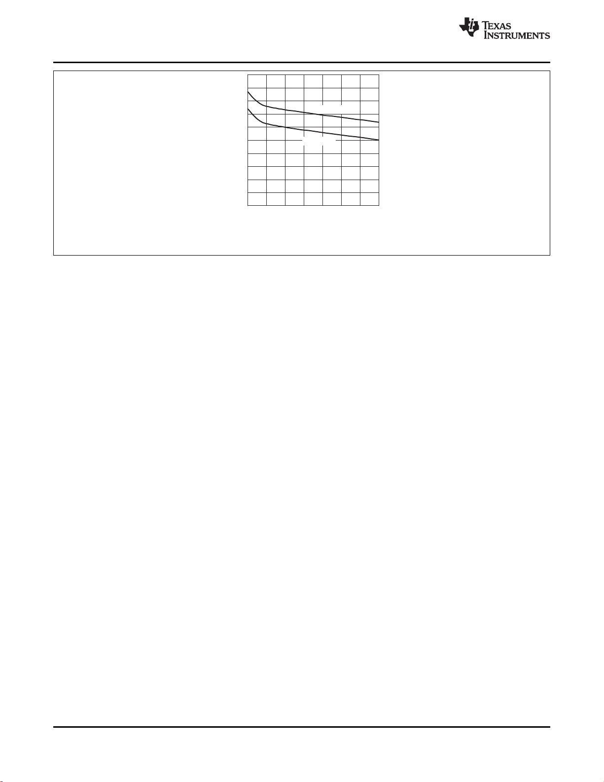
V
O
5 V/div
EN
1 V/div
I
I
50 mA/div
VO= 18 V
500 us/div
V
I
2.4 V to 3.4 V
V
O
100 mV/div
200 µS/div
VO = 18 V
I
O
1 mA to 10 mA
200 mS/div
I
O
100 mV/div
IO= 18 V
www.ti.com
9.2.3 Application Curves
TPS61040,TPS61041
SLVS413H –OCTOBER 2002–REVISED OCTOBER 2015
Figure 13. Line Transient Response
Figure 14. Load Transient Response
Figure 15. Start-Up Behavior
Copyright © 2002–2015, Texas Instruments Incorporated Submit Documentation Feedback 15
Product Folder Links: TPS61040 TPS61041

V
IN
SW
FB
EN
GND
L1
6.8 µH
D1
R1
1.5 MW
R2
210 kW
C
FF
22 pF
C2
1 µF
V1 = 10 V/15 mA
VIN = 2.7 V to 5 V
C1
4.7 µF
C4
4.7 µF
C3
1 µF
V2 = –10 V/15 mA
D2
D3
L1: Murata LQH4C6R8M04
D1, D2, D3: Motorola MBR0530
C1: Tayo Yuden JMK212BY475MG
C2, C3, C4: Tayo Yuden EMK316BJ105KF
TPS61040
V
IN
SW
FB
EN
GND
L1
10 µH
D1
R1
2.2 MW
R2
160 kW
C
FF
22 pF
C2
1 µF
V
OUT
18 V / 10 mA
V
IN
1.8 V to 6 V
C1
4.7 µF
R3
200 kW
BC857C
C3
0.1 µF
(Optional)
L1: Sumida CR32-100
D1: Motorola MBR0530
C1: Tayo Yuden JMK212BY475MG
C2: Tayo Yuden TMK316BJ105KL
TPS61040
V
IN
SW
FB
EN
GND
L1
10 µH
D1
R1
2.2 MW
R2
160 kW
C
FF
22 pF
C2
1 µF
V
O
18 V
VIN
1.8 V to 6 V
C1
4.7 µF
DAC or Analog Voltage
0 V = 25 V
1.233 V = 18 V
TPS61040
L1: Sumida CR32-100
D1: Motorola MBR0530
C1: Tayo Yuden JMK212BY475MG
C2: Tayo Yuden GMK316BJ105KL
TPS61040,TPS61041
SLVS413H –OCTOBER 2002–REVISED OCTOBER 2015
9.3 System Examples
Figure 16. LCD Bias Supply With Adjustable Output Voltage
www.ti.com
16 Submit Documentation Feedback Copyright © 2002–2015, Texas Instruments Incorporated
Figure 17. LCD Bias Supply With Load Disconnect
Figure 18. Positive and Negative Output LCD Bias Supply
Product Folder Links: TPS61040 TPS61041

V
IN
SW
FB
EN
GND
L1
10 µH
D1
C2
1 µF
C1
4.7 µF
R
S
82 Ω
VCC = 2.7 V to 6 V
PWM
100 Hz to 500 Hz
D2
24 V
(Optional)
L1: Murata LQH4C100K04
D1: Motorola MBR0530
C1: Tayo Yuden JMK212BY475MG
C2: Tayo Yuden TMK316BJ105KL
V
IN
SW
FB
EN
GND
3.3 µH
D1
C2
4.7 µF
5 V/45 mA
1.8 V to 4 V
C1
4.7 µF
TPS61040
L1: Murata LQH4C3R3M04
D1: Motorola MBR0530
C1, C2: Tayo Yuden JMK212BY475MG
C
FF
3.3 pF
R1
620 kW
R2
200 kW
V
IN
SW
FB
EN
GND
L1
6.8 µH
D1
R1
1.8 MW
R2
205 kW
C
FF
4.7 pF
C2
4.7 µF
V
O =
12 V/35 mA
VIN 3.3 V
C1
10 µF
L1: Murata LQH4C6R8M04
D1: Motorola MBR0530
C1: Tayo Yuden JMK212BJ106MG
C2: Tayo Yuden EMK316BJ475ML
TPS61040
www.ti.com
System Examples (continued)
TPS61040,TPS61041
SLVS413H –OCTOBER 2002–REVISED OCTOBER 2015
Figure 19. Standard 3.3-V to 12-V Supply
Figure 20. Dual Battery Cell to 5-V/50-mA Conversion
Efficiency Approximately Equals 84% at VIN= 2.4 V to Vo = 5 V/45 mA
Figure 21. White LED Supply With Adjustable Brightness Control
Using a PWM Signal on the Enable Pin, Efficiency Approximately Equals 86% at VIN= 3 V, I
Copyright © 2002–2015, Texas Instruments Incorporated Submit Documentation Feedback 17
Product Folder Links: TPS61040 TPS61041
LED
= 15 mA

V
IN
SW
FB
EN
GND
L1
10 µH
D1
MBRM120L
C2
100 nF
(See
Note A)
C1
4.7 µF
R
S
110 Ω
VCC = 2.7 V to 6 V
R1
120 kΩ
R2
160 kΩ
Analog Brightness Control
3.3 V ≅ Led Off
0 V ≅ Iled = 20 mA
D2
24 V
(Optional)
L1: Murata LQH4C3R3M04
D1: Motorola MBR0530
C1: Tayo Yuden JMK212BY475MG
C2: Standard Ceramic Capacitor
TPS61040,TPS61041
SLVS413H –OCTOBER 2002–REVISED OCTOBER 2015
System Examples (continued)
A. A smaller output capacitor value for C2 causes a larger LED ripple.
Figure 22. White LED Supply With Adjustable Brightness Control
Using an Analog Signal on the Feedback Pin
www.ti.com
18 Submit Documentation Feedback Copyright © 2002–2015, Texas Instruments Incorporated
Product Folder Links: TPS61040 TPS61041
VIN1
2
3
4
FB
EN
5
TPS61040
SW
GND
VIN
VOUT
GND
TPS61040,TPS61041
www.ti.com
SLVS413H –OCTOBER 2002–REVISED OCTOBER 2015
10 Power Supply Recommendations
The device is designed to operate from an input voltage supply range between 1.8 V and 6 V. The output current
of the input power supply must be rated according to the supply voltage, output voltage and output current of
TPS6104x.
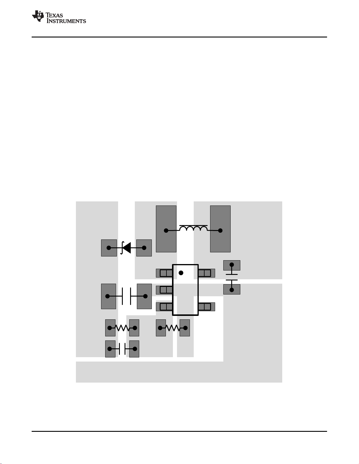
11 Layout
11.1 Layout Guidelines
Typical for all switching power supplies, the layout is an important step in the design; especially at high peak
currents and switching frequencies. If the layout is not carefully done, the regulator might show noise problems
and duty cycle jitter.
The input capacitor should be placed as close as possible to the input pin for good input voltage filtering. The
inductor and diode should be placed as close as possible to the switch pin to minimize the noise coupling into
other circuits. Because the feedback pin and network is a high-impedance circuit, the feedback network should
be routed away from the inductor. The feedback pin and feedback network should be shielded with a ground
plane or trace to minimize noise coupling into this circuit.
Wide traces should be used for connections in bold as shown in Figure 23. A star ground connection or ground
plane minimizes ground shifts and noise.
11.2 Layout Example
Copyright © 2002–2015, Texas Instruments Incorporated Submit Documentation Feedback 19
Figure 23. Layout Diagram
Product Folder Links: TPS61040 TPS61041
TPS61040,TPS61041
SLVS413H –OCTOBER 2002–REVISED OCTOBER 2015
www.ti.com
12 Device and Documentation Support
12.1 Third-Party Products Disclaimer
TI'S PUBLICATION OF INFORMATION REGARDING THIRD-PARTY PRODUCTS OR SERVICES DOES NOT
CONSTITUTE AN ENDORSEMENT REGARDING THE SUITABILITY OF SUCH PRODUCTS OR SERVICES
OR A WARRANTY, REPRESENTATION OR ENDORSEMENT OF SUCH PRODUCTS OR SERVICES, EITHER
ALONE OR IN COMBINATION WITH ANY TI PRODUCT OR SERVICE.
12.2 Related Links
The table below lists quick access links. Categories include technical documents, support and community
resources, tools and software, and quick access to sample or buy.
Table 6. Related Links
PARTS PRODUCT FOLDER SAMPLE & BUY
TPS61041 Click here Click here Click here Click here Click here
TPS61040 Click here Click here Click here Click here Click here
12.3 Community Resources
The following links connect to TI community resources. Linked contents are provided "AS IS" by the respective
contributors. They do not constitute TI specifications and do not necessarily reflect TI's views; see TI's Terms of
Use.
TI E2E™ Online Community TI's Engineer-to-Engineer (E2E) Community. Created to foster collaboration
among engineers. At e2e.ti.com, you can ask questions, share knowledge, explore ideas and help
solve problems with fellow engineers.
Design Support TI's Design Support Quickly find helpful E2E forums along with design support tools and
contact information for technical support.
TECHNICAL TOOLS & SUPPORT &
DOCUMENTS SOFTWARE COMMUNITY
12.4 Trademarks
E2E is a trademark of Texas Instruments.
All other trademarks are the property of their respective owners.
12.5 Electrostatic Discharge Caution
These devices have limited built-in ESD protection. The leads should be shorted together or the device placed in conductive foam
during storage or handling to prevent electrostatic damage to the MOS gates.
12.6 Glossary
SLYZ022 — TI Glossary.
This glossary lists and explains terms, acronyms, and definitions.
13 Mechanical, Packaging, and Orderable Information
The following pages include mechanical, packaging, and orderable information. This information is the most
current data available for the designated devices. This data is subject to change without notice and revision of
this document. For browser-based versions of this data sheet, refer to the left-hand navigation.
20 Submit Documentation Feedback Copyright © 2002–2015, Texas Instruments Incorporated
Product Folder Links: TPS61040 TPS61041

PACKAGE OPTION ADDENDUM
www.ti.com
PACKAGING INFORMATION
Orderable Device Status
TPS61040DBVR ACTIVE SOT-23 DBV 5 3000 Green (RoHS
TPS61040DBVRG4 ACTIVE SOT-23 DBV 5 3000 Green (RoHS
TPS61040DDCR ACTIVE SOT DDC 5 3000 Green (RoHS
TPS61040DDCT ACTIVE SOT DDC 5 250 Green (RoHS
TPS61040DRVR ACTIVE SON DRV 6 3000 Green (RoHS
TPS61040DRVT ACTIVE SON DRV 6 250 Green (RoHS
TPS61040DRVTG4 ACTIVE SON DRV 6 250 Green (RoHS
TPS61041DBVR ACTIVE SOT-23 DBV 5 3000 Green (RoHS
TPS61041DBVRG4 ACTIVE SOT-23 DBV 5 3000 Green (RoHS
TPS61041DRVR ACTIVE SON DRV 6 3000 Green (RoHS
TPS61041DRVRG4 ACTIVE SON DRV 6 3000 Green (RoHS
TPS61041DRVT ACTIVE SON DRV 6 250 Green (RoHS
TPS61041DRVTG4 ACTIVE SON DRV 6 250 Green (RoHS
(1)
The marketing status values are defined as follows:
ACTIVE: Product device recommended for new designs.
LIFEBUY: TI has announced that the device will be discontinued, and a lifetime-buy period is in effect.
NRND: Not recommended for new designs. Device is in production to support existing customers, but TI does not recommend using this part in a new design.
PREVIEW: Device has been announced but is not in production. Samples may or may not be available.
OBSOLETE: TI has discontinued the production of the device.
Package Type Package
(1)
Drawing
Pins Package
Qty
Eco Plan
(2)
& no Sb/Br)
& no Sb/Br)
& no Sb/Br)
& no Sb/Br)
& no Sb/Br)
& no Sb/Br)
& no Sb/Br)
& no Sb/Br)
& no Sb/Br)
& no Sb/Br)
& no Sb/Br)
& no Sb/Br)
& no Sb/Br)
Lead/Ball Finish
(6)
MSL Peak Temp
(3)
CU NIPDAU Level-1-260C-UNLIM -40 to 85 PHOI
CU NIPDAU Level-1-260C-UNLIM -40 to 85 PHOI
CU NIPDAU Level-2-260C-1 YEAR -40 to 85 QXK
CU NIPDAU Level-2-260C-1 YEAR -40 to 85 QXK
CU NIPDAU Level-1-260C-UNLIM -40 to 85 CCL
CU NIPDAU Level-1-260C-UNLIM -40 to 85 CCL
CU NIPDAU Level-1-260C-UNLIM -40 to 85 CCL
CU NIPDAU Level-1-260C-UNLIM -40 to 85 PHPI
CU NIPDAU Level-1-260C-UNLIM -40 to 85 PHPI
CU NIPDAU Level-1-260C-UNLIM -40 to 85 CAW
CU NIPDAU Level-1-260C-UNLIM -40 to 85 CAW
CU NIPDAU Level-1-260C-UNLIM -40 to 85 CAW
CU NIPDAU Level-1-260C-UNLIM -40 to 85 CAW
5-Oct-2015
Op Temp (°C) Device Marking
(4/5)
Samples
Addendum-Page 1
PACKAGE OPTION ADDENDUM
www.ti.com
(2)
Eco Plan - The planned eco-friendly classification: Pb-Free (RoHS), Pb-Free (RoHS Exempt), or Green (RoHS & no Sb/Br) - please check http://www.ti.com/productcontent for the latest availability
information and additional product content details.
TBD: The Pb-Free/Green conversion plan has not been defined.
Pb-Free (RoHS): TI's terms "Lead-Free" or "Pb-Free" mean semiconductor products that are compatible with the current RoHS requirements for all 6 substances, including the requirement that
lead not exceed 0.1% by weight in homogeneous materials. Where designed to be soldered at high temperatures, TI Pb-Free products are suitable for use in specified lead-free processes.
Pb-Free (RoHS Exempt): This component has a RoHS exemption for either 1) lead-based flip-chip solder bumps used between the die and package, or 2) lead-based die adhesive used between
the die and leadframe. The component is otherwise considered Pb-Free (RoHS compatible) as defined above.
Green (RoHS & no Sb/Br): TI defines "Green" to mean Pb-Free (RoHS compatible), and free of Bromine (Br) and Antimony (Sb) based flame retardants (Br or Sb do not exceed 0.1% by weight
in homogeneous material)
(3)
MSL, Peak Temp. - The Moisture Sensitivity Level rating according to the JEDEC industry standard classifications, and peak solder temperature.
(4)
There may be additional marking, which relates to the logo, the lot trace code information, or the environmental category on the device.
(5)
Multiple Device Markings will be inside parentheses. Only one Device Marking contained in parentheses and separated by a "~" will appear on a device. If a line is indented then it is a continuation
of the previous line and the two combined represent the entire Device Marking for that device.
(6)
Lead/Ball Finish - Orderable Devices may have multiple material finish options. Finish options are separated by a vertical ruled line. Lead/Ball Finish values may wrap to two lines if the finish
value exceeds the maximum column width.
Important Information and Disclaimer:The information provided on this page represents TI's knowledge and belief as of the date that it is provided. TI bases its knowledge and belief on information
provided by third parties, and makes no representation or warranty as to the accuracy of such information. Efforts are underway to better integrate information from third parties. TI has taken and
continues to take reasonable steps to provide representative and accurate information but may not have conducted destructive testing or chemical analysis on incoming materials and chemicals.
TI and TI suppliers consider certain information to be proprietary, and thus CAS numbers and other limited information may not be available for release.
In no event shall TI's liability arising out of such information exceed the total purchase price of the TI part(s) at issue in this document sold by TI to Customer on an annual basis.
OTHER QUALIFIED VERSIONS OF TPS61040, TPS61041 :
Automotive: TPS61040-Q1, TPS61041-Q1
•
5-Oct-2015
NOTE: Qualified Version Definitions:
Automotive - Q100 devices qualified for high-reliability automotive applications targeting zero defects
•
Addendum-Page 2
PACKAGE MATERIALS INFORMATION
www.ti.com 6-Oct-2015
TAPE AND REEL INFORMATION
*All dimensions are nominal
Device Package
TPS61040DBVR SOT-23 DBV 5 3000 178.0 9.0 3.23 3.17 1.37 4.0 8.0 Q3
TPS61040DBVR SOT-23 DBV 5 3000 179.0 8.4 3.2 3.2 1.4 4.0 8.0 Q3
TPS61040DDCR SOT DDC 5 3000 179.0 8.4 3.2 3.2 1.4 4.0 8.0 Q3
TPS61040DDCT SOT DDC 5 250 179.0 8.4 3.2 3.2 1.4 4.0 8.0 Q3
TPS61040DRVR SON DRV 6 3000 179.0 8.4 2.2 2.2 1.2 4.0 8.0 Q2
TPS61040DRVT SON DRV 6 250 179.0 8.4 2.2 2.2 1.2 4.0 8.0 Q2
TPS61041DBVR SOT-23 DBV 5 3000 178.0 9.0 3.23 3.17 1.37 4.0 8.0 Q3
TPS61041DBVR SOT-23 DBV 5 3000 179.0 8.4 3.2 3.2 1.4 4.0 8.0 Q3
TPS61041DRVR SON DRV 6 3000 179.0 8.4 2.2 2.2 1.2 4.0 8.0 Q2
Type
Package
Drawing
Pins SPQ Reel
Diameter
(mm)
Reel
Width
W1 (mm)
A0
(mm)B0(mm)K0(mm)P1(mm)W(mm)
Pin1
Quadrant
Pack Materials-Page 1
PACKAGE MATERIALS INFORMATION
www.ti.com 6-Oct-2015
*All dimensions are nominal
Device Package Type Package Drawing Pins SPQ Length (mm) Width (mm) Height (mm)
TPS61040DBVR SOT-23 DBV 5 3000 180.0 180.0 18.0
TPS61040DBVR SOT-23 DBV 5 3000 203.0 203.0 35.0
TPS61040DDCR SOT DDC 5 3000 195.0 200.0 45.0
TPS61040DDCT SOT DDC 5 250 195.0 200.0 45.0
TPS61040DRVR SON DRV 6 3000 203.0 203.0 35.0
TPS61040DRVT SON DRV 6 250 203.0 203.0 35.0
TPS61041DBVR SOT-23 DBV 5 3000 180.0 180.0 18.0
TPS61041DBVR SOT-23 DBV 5 3000 203.0 203.0 35.0
TPS61041DRVR SON DRV 6 3000 203.0 203.0 35.0
Pack Materials-Page 2


IMPORTANT NOTICE
Texas Instruments Incorporated and its subsidiaries (TI) reserve the right to make corrections, enhancements, improvements and other
changes to its semiconductor products and services per JESD46, latest issue, and to discontinue any product or service per JESD48, latest
issue. Buyers should obtain the latest relevant information before placing orders and should verify that such information is current and
complete. All semiconductor products (also referred to herein as “components”) are sold subject to TI’s terms and conditions of sale
supplied at the time of order acknowledgment.
TI warrants performance of its components to the specifications applicable at the time of sale, in accordance with the warranty in TI’s terms
and conditions of sale of semiconductor products. Testing and other quality control techniques are used to the extent TI deems necessary
to support this warranty. Except where mandated by applicable law, testing of all parameters of each component is not necessarily
performed.
TI assumes no liability for applications assistance or the design of Buyers’ products. Buyers are responsible for their products and
applications using TI components. To minimize the risks associated with Buyers’ products and applications, Buyers should provide
adequate design and operating safeguards.
TI does not warrant or represent that any license, either express or implied, is granted under any patent right, copyright, mask work right, or
other intellectual property right relating to any combination, machine, or process in which TI components or services are used. Information
published by TI regarding third-party products or services does not constitute a license to use such products or services or a warranty or
endorsement thereof. Use of such information may require a license from a third party under the patents or other intellectual property of the
third party, or a license from TI under the patents or other intellectual property of TI.
Reproduction of significant portions of TI information in TI data books or data sheets is permissible only if reproduction is without alteration
and is accompanied by all associated warranties, conditions, limitations, and notices. TI is not responsible or liable for such altered
documentation. Information of third parties may be subject to additional restrictions.
Resale of TI components or services with statements different from or beyond the parameters stated by TI for that component or service
voids all express and any implied warranties for the associated TI component or service and is an unfair and deceptive business practice.
TI is not responsible or liable for any such statements.
Buyer acknowledges and agrees that it is solely responsible for compliance with all legal, regulatory and safety-related requirements
concerning its products, and any use of TI components in its applications, notwithstanding any applications-related information or support
that may be provided by TI. Buyer represents and agrees that it has all the necessary expertise to create and implement safeguards which
anticipate dangerous consequences of failures, monitor failures and their consequences, lessen the likelihood of failures that might cause
harm and take appropriate remedial actions. Buyer will fully indemnify TI and its representatives against any damages arising out of the use
of any TI components in safety-critical applications.
In some cases, TI components may be promoted specifically to facilitate safety-related applications. With such components, TI’s goal is to
help enable customers to design and create their own end-product solutions that meet applicable functional safety standards and
requirements. Nonetheless, such components are subject to these terms.
No TI components are authorized for use in FDA Class III (or similar life-critical medical equipment) unless authorized officers of the parties
have executed a special agreement specifically governing such use.
Only those TI components which TI has specifically designated as military grade or “enhanced plastic” are designed and intended for use in
military/aerospace applications or environments. Buyer acknowledges and agrees that any military or aerospace use of TI components
which have not been so designated is solely at the Buyer's risk, and that Buyer is solely responsible for compliance with all legal and
regulatory requirements in connection with such use.
TI has specifically designated certain components as meeting ISO/TS16949 requirements, mainly for automotive use. In any case of use of
non-designated products, TI will not be responsible for any failure to meet ISO/TS16949.
Products Applications
Audio www.ti.com/audio Automotive and Transportation www.ti.com/automotive
Amplifiers amplifier.ti.com Communications and Telecom www.ti.com/communications
Data Converters dataconverter.ti.com Computers and Peripherals www.ti.com/computers
DLP® Products www.dlp.com Consumer Electronics www.ti.com/consumer-apps
DSP dsp.ti.com Energy and Lighting www.ti.com/energy
Clocks and Timers www.ti.com/clocks Industrial www.ti.com/industrial
Interface interface.ti.com Medical www.ti.com/medical
Logic logic.ti.com Security www.ti.com/security
Power Mgmt power.ti.com Space, Avionics and Defense www.ti.com/space-avionics-defense
Microcontrollers microcontroller.ti.com Video and Imaging www.ti.com/video
RFID www.ti-rfid.com
OMAP Applications Processors www.ti.com/omap TI E2E Community e2e.ti.com
Wireless Connectivity www.ti.com/wirelessconnectivity
Mailing Address: Texas Instruments, Post Office Box 655303, Dallas, Texas 75265
Copyright © 2015, Texas Instruments Incorporated

 Loading...