

Texas Instruments TPS61030PWP, TPS61030RSAR, TPS61031PWP, TPS61031RSAR, TPS61032PWP Schematic [ru]
...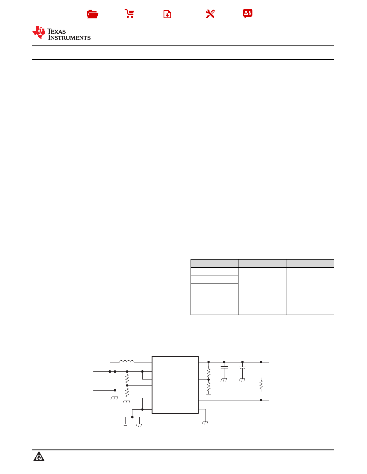
SW
C1
10 µF
L1
6.8 µH
R1
R2
VBAT
VOUT
FB
C2
2.2 µFC3220 µF
LBO
PGND
LBI
SYNC
EN
GND
TPS6103x
e.g. 5 V up to
1000 mA
Low Battery
Comparator
Output
R3
R4
R6
1.8 V to 5 V
Input
Product
Folder
Sample &
Buy
Technical
Documents
Tools &
Software
Support &
Community
SLUS534G –SEPTEMBER 2002–REVISED MARCH 2015
TPS6103x 96% Efficient Synchronous Boost Converter With 4A Switch
1 Features 3 Description
1
• 96% Efficient Synchronous Boost Converter With
1000-mA Output Current
From 1.8-V Input
• Device Quiescent Current: 20-µA (Typ)
• Input Voltage Range: 1.8-V to 5.5-V
• Fixed and Adjustable Output Voltage Options Up
to 5.5-V
• Power Save Mode for Improved Efficiency at Low
Output Power
• Low Battery Comparator
• Low EMI-Converter (Integrated Antiringing Switch)
• Load Disconnect During Shutdown
• Over-Temperature Protection
• Available in a Small 4 mm x 4 mm QFN-16 or in a
TSSOP-16 Package
2 Applications
All Single Cell Li or Dual Cell Battery Operated
Products as MP-3 Player, PDAs, and Other
Portable Equipment
The TPS6103x devices provide a power supply
solution for products powered by either a one-cell LiIon or Li-polymer, or a two to three-cell alkaline, NiCd
or NiMH battery. The converter generates a stable
output voltage that is either adjusted by an external
resistor divider or fixed internally on the chip. It
provides high efficient power conversion and is
capable of delivering output currents up to 1 A at 5 V
at a supply voltage down to 1.8 V. The implemented
boost converter is based on a fixed frequency, pulsewidth- modulation (PWM) controller using a
synchronous rectifier to obtain maximum efficiency.
At low load currents the converter enters Power Save
mode to maintain a high efficiency over a wide load
current range. The Power Save mode can be
disabled, forcing the converter to operate at a fixed
switching frequency. It can also operate synchronized
to an external clock signal that is applied to the
SYNC pin. The maximum peak current in the boost
switch is limited to a value of 4500 mA.
The converter can be disabled to minimize battery
drain. During shutdown, the load is completely
disconnected from the battery. A low-EMI mode is
implemented to reduce ringing and, in effect, lower
radiated electromagnetic energy when the converter
enters the discontinuous conduction mode.
TPS61030,TPS61031,TPS61032
4 Simplified Schematic
1
An IMPORTANT NOTICE at the end of this data sheet addresses availability, warranty, changes, use in safety-critical applications,
intellectual property matters and other important disclaimers. PRODUCTION DATA.
Device Information
PART NUMBER PACKAGE BODY SIZE (NOM)
TPS61030
TPS61031 TSSOP (16) 5.00 mm × 4.40 mm
TPS61032
TPS61030
TPS61031 QFN (16) 4.00 mm x 4.00 mm
TPS61032
(1) For all available packages, see the orderable addendum at
the end of the datasheet.
(1)

TPS61030,TPS61031,TPS61032
SLUS534G –SEPTEMBER 2002–REVISED MARCH 2015
www.ti.com
Table of Contents
1 Features.................................................................. 1
2 Applications ........................................................... 1
3 Description ............................................................. 1
4 Simplified Schematic............................................. 1
5 Revision History..................................................... 2
6 Device Comparison Table..................................... 3
7 Pin Configuration and Functions......................... 3
8 Specifications......................................................... 4
8.1 Absolute Maximum Ratings ...................................... 4
8.2 ESD Ratings ............................................................ 4
8.3 Recommended Operating Conditions....................... 4
8.4 Thermal Information.................................................. 4
8.5 Electrical Characteristics........................................... 5
8.6 Typical Characteristics.............................................. 6
9 Parameter Measurement Information .................. 8
10 Detailed Description ............................................. 9
10.1 Overview................................................................. 9
10.2 Functional Block Diagram....................................... 9
10.3 Feature Description............................................... 10
10.4 Device Functional Modes...................................... 10
11 Application and Implementation........................ 12
11.1 Application Information.......................................... 12
11.2 Typical Application ............................................... 12
12 Power Supply Recommendations ..................... 18
13 Layout................................................................... 18
13.1 Layout Considerations .......................................... 18
13.2 Layout Example .................................................... 18
13.3 Thermal Considerations........................................ 18
14 Device and Documentation Support ................. 19
14.1 Device Support...................................................... 19
14.2 Related Links ........................................................ 19
14.3 Trademarks........................................................... 19
14.4 Electrostatic Discharge Caution............................ 19
14.5 Glossary................................................................ 19
15 Mechanical, Packaging, and Orderable
Information........................................................... 19
5 Revision History
NOTE: Page numbers for previous revisions may differ from page numbers in the current version.
Changes from Revision F (October 2014) to Revision G Page
• Moved T
spec to the Absolute Maximum Ratings table. Changed Handling Ratings to ESD Ratings............................... 4
stg
• Added System Examples .................................................................................................................................................... 16
Changes from Revision E (January 2012) to Revision F Page
• Added Device Information and Handling Rating tables, Feature Description section, Device Functional Modes,
Application and Implementation section, Power Supply Recommendations section, Layout section, Device and
Documentation Support section, and Mechanical, Packaging, and Orderable Information section ..................................... 1
Changes from Revision D (April 2004) to Revision E Page
• Changed the temperature range From: 40°C to 85°C To: -40°C to 85°C.............................................................................. 3
2 Submit Documentation Feedback Copyright © 2002–2015, Texas Instruments Incorporated
Product Folder Links: TPS61030 TPS61031 TPS61032
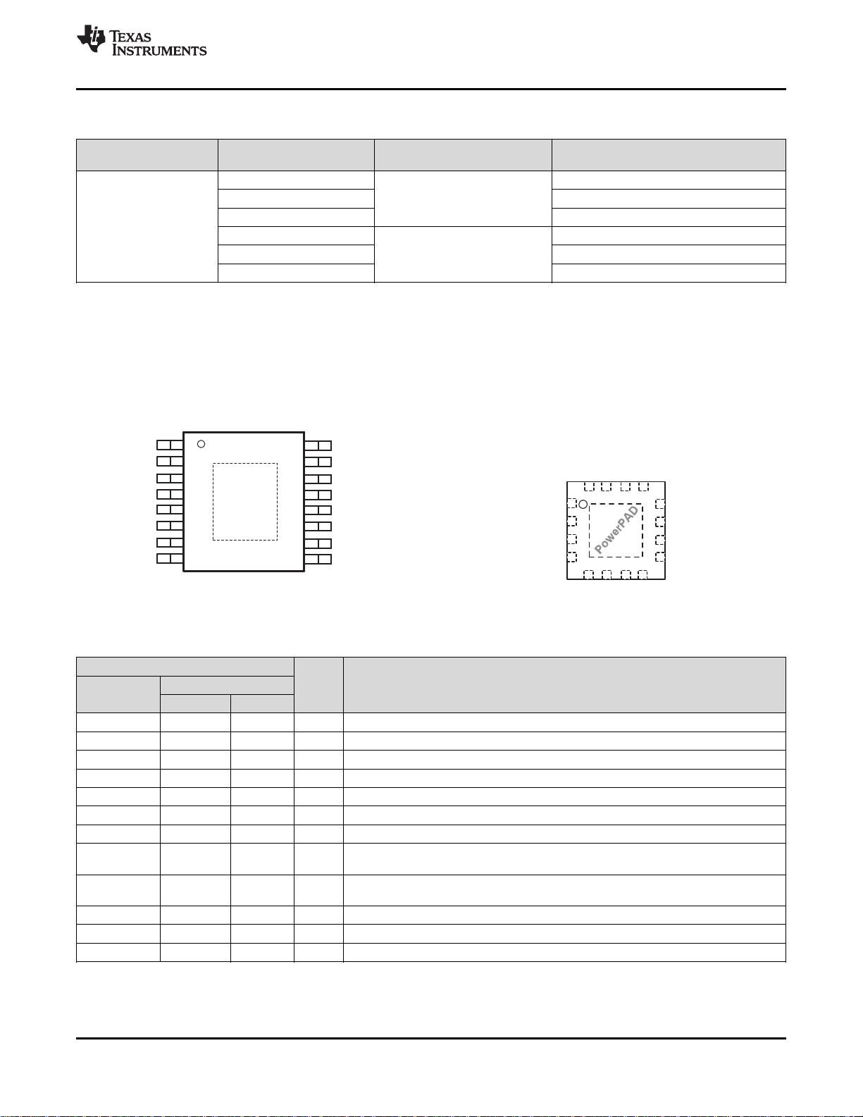
NC
SW
SW
LBI
LBO
VOUT
SYNC
EN
VBAT
VOUT
VOUT
FB
GND
1
2
3
4
5
6
7
8
16
15
14
13
12
11
10
9
SW
SW
VBAT
LBI
SYNC
NC
VOUT
VOUT
VOUT
FB
GND
LBO
EN
NC − No internal connection
PowerPAD
www.ti.com
TPS61030,TPS61031,TPS61032
SLUS534G –SEPTEMBER 2002–REVISED MARCH 2015
DC/DC
(1)
PACKAGE PART NUMBER
6 Device Comparison Table
T
A
-40°C to 85°C
(1) Contact the factory to check availability of other fixed output voltage versions.
(1) For all available packages, see the orderable addendum at the end of the datasheet.
OUTPUT VOLTAGE
Adjustable TPS61030
3.3 V 16-Pin TSSOP PowerPAD™ TPS61031
5 V TPS61032
Adjustable TPS61030
3.3 V 16-Pin QFN TPS61031
5 V TPS61032
7 Pin Configuration and Functions
PWP Package
16-Pins
Top View
(1)
RSA Package
16-Pins
Top View
Pin Functions
PIN
NAME
EN 9 11 I Enable input. (1/VBAT enabled, 0/GND disabled)
FB 12 14 I Voltage feedback of adjustable versions
GND 11 13 I/O Control/logic ground
LBI 7 9 I Low battery comparator input (comparator enabled with EN)
LBO 10 12 O Low battery comparator output (open drain)
NC 16 2 Not connected
PGND 3, 4, 5 5, 6, 7 I/O Power ground
PowerPAD™ Must be soldered to achieve appropriate power dissipation. Should be connected to
SYNC 8 10 I Enable/disable power save mode (1/VBAT disabled, 0/GND enabled, clock signal for
SW 1, 2 3, 4 I Boost and rectifying switch input
VBAT 6 8 I Supply voltage
VOUT 13, 14, 15 1, 15, 16 O DC/DC output
Copyright © 2002–2015, Texas Instruments Incorporated Submit Documentation Feedback 3
NO. I/O DESCRIPTION
PWP RSA
PGND.
synchronization)
Product Folder Links: TPS61030 TPS61031 TPS61032
TPS61030,TPS61031,TPS61032
SLUS534G –SEPTEMBER 2002–REVISED MARCH 2015
www.ti.com
8 Specifications
8.1 Absolute Maximum Ratings
over operating free-air temperature range (unless otherwise noted)
VIInput voltage on LBI –0.3 3.6 V
Input voltage on SW, VOUT, LBO, VBAT, SYNC, EN, FB –0.3 7 V
TJMaximum junction temperature –40 150
T
Storage temperature range –65 150
stg
(1) Stresses beyond those listed under Absolute Maximum Ratings may cause permanent damage to the device. These are stress ratings
only, and functional operation of the device at these or any other conditions beyond those indicated under Recommended Operating
Conditions is not implied. Exposure to absolute-maximum-rated conditions for extended periods may affect device reliability.
8.2 ESD Ratings
Human body model (HBM), per ANSI/ESDA/JEDEC JS-001, all –2000 2000
(1)
V
Electrostatic discharge V
(ESD)
(1) JEDEC document JEP155 states that 500-V HBM allows safe manufacturing with a standard ESD control process.
(2) JEDEC document JEP157 states that 250-V CDM allows safe manufacturing with a standard ESD control process.
pins
Charged device model (CDM), per JEDEC specification JESD22- –1000 1000
C101, all pins
(2)
(1)
MIN MAX UNIT
°C
MIN MAX UNIT
8.3 Recommended Operating Conditions
MIN NOM MAX UNIT
V
T
T
Supply voltage at VBAT 1.8 5.5 V
I
Operating ambient temperature range -40 85 °C
A
Operating virtual junction temperature range -40 125 °C
J
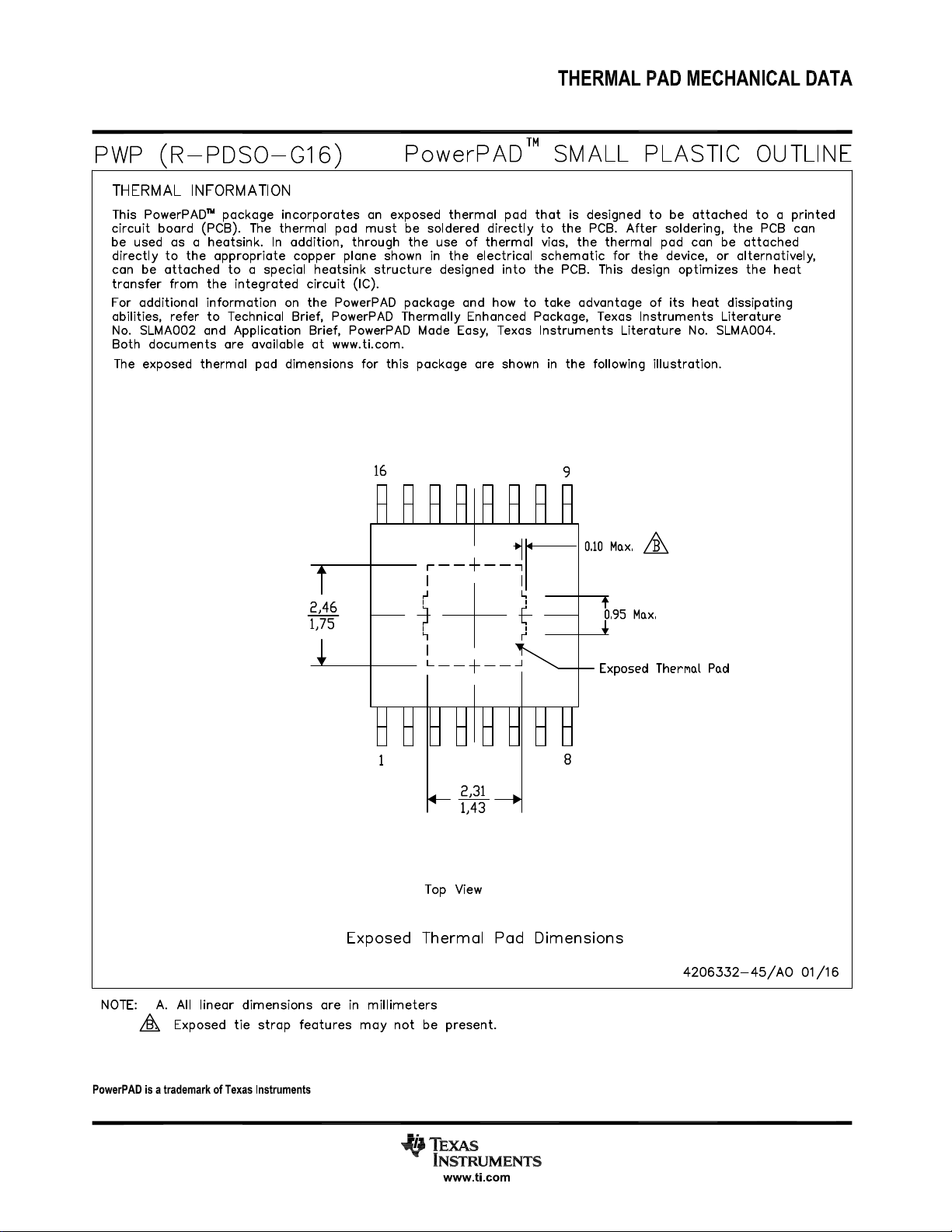
8.4 Thermal Information
TPS6103x
THERMAL METRIC
R
θJA
R
θJC(top)
R
θJB
ψ
JT
ψ
JB
R
θJC(bot)
Junction-to-ambient thermal resistance 46.9 35.5
Junction-to-case (top) thermal resistance 25.8 36.7
Junction-to-board thermal resistance 19.4 12.9
Junction-to-top characterization parameter 0.8 0.5
Junction-to-board characterization parameter 19.3 12.9
Junction-to-case (bottom) thermal resistance 2.2 3.8
(1) For more information about traditional and new thermal metrics, see the IC Package Thermal Metrics application report, SPRA953.
(1)
PWP RSA UNIT
16 PINS 16 PINS
°C/W
4 Submit Documentation Feedback Copyright © 2002–2015, Texas Instruments Incorporated
Product Folder Links: TPS61030 TPS61031 TPS61032
TPS61030,TPS61031,TPS61032
www.ti.com
SLUS534G –SEPTEMBER 2002–REVISED MARCH 2015
8.5 Electrical Characteristics
over recommended free-air temperature range and over recommended input voltage range (typical at an ambient temperature
range of 25°C) (unless otherwise noted)
PARAMETER TEST CONDITIONS MIN TYP MAX UNIT
DC/DC STAGE
V
Input voltage range 1.8 5.5 V
I
V
TPS61030 output voltage range 1.8 5.5 V
O
V
TPS61030 feedback voltage 490 500 510 mV
FB
f Oscillator frequency 500 600 700 kHz
Frequency range for synchronization 500 700 kHz
Switch current limit VOUT= 5 V 3600 4000 4500 mA
Start-up current limit 0.4 x I
SW
SWN switch on resistance VOUT= 5 V 55 mΩ
SWP switch on resistance VOUT= 5 V 55 mΩ
Total accuracy -3% 3%
Line regulation 0.6%
Load regulation 0.6%
VBAT 10 25 µA
Quiescent current
VOUT 10 20 µA
IO= 0 mA, VEN= VBAT = 1.8 V,
VOUT =5 V
IO= 0 mA, VEN= VBAT = 1.8 V,
VOUT = 5 V
Shutdown current VEN= 0 V, VBAT = 2.4 V 0.1 1 µA
CONTROL STAGE
V
Under voltage lockout threshold V
UVLO
V
LBI voltage threshold V
IL
voltage decreasing 1.5 V
LBI
voltage decreasing 490 500 510 mV
LBI
LBI input hysteresis 10 mV
LBI input current EN = VBAT or GND 0.01 0.1 µA
LBO output low voltage VO= 3.3 V, IOI= 100 µA 0.04 0.4 V
LBO output low current 100 µA
LBO output leakage current V
V
EN, SYNC input low voltage 0.2 × VBAT V
IL
V
EN, SYNC input high voltage 0.8 × VBAT V
IH
= 7 V 0.01 0.1 µA
LBO
EN, SYNC input current Clamped on GND or VBAT 0.01 0.1 µA
Overtemperature protection 140 °C
Overtemperature hysteresis 20 °C
mA
Copyright © 2002–2015, Texas Instruments Incorporated Submit Documentation Feedback 5
Product Folder Links: TPS61030 TPS61031 TPS61032
0
0.5
1
1.5
2
2.5
3
3.5
1.8 2.2 2.6 3 3.4 3.8 4.2 4.6 5
V
- Input Voltage - V
Maximum Output Current
- A
0
0.5
1
1.5
2
2.5
3
3.5
1.8 2.2 2.6 3 3.4 3.8 4.2 4.6 5
V
- Input Voltage - V
Maximum Output Current
- A
TPS61030,TPS61031,TPS61032
SLUS534G –SEPTEMBER 2002–REVISED MARCH 2015
www.ti.com
8.6 Typical Characteristics
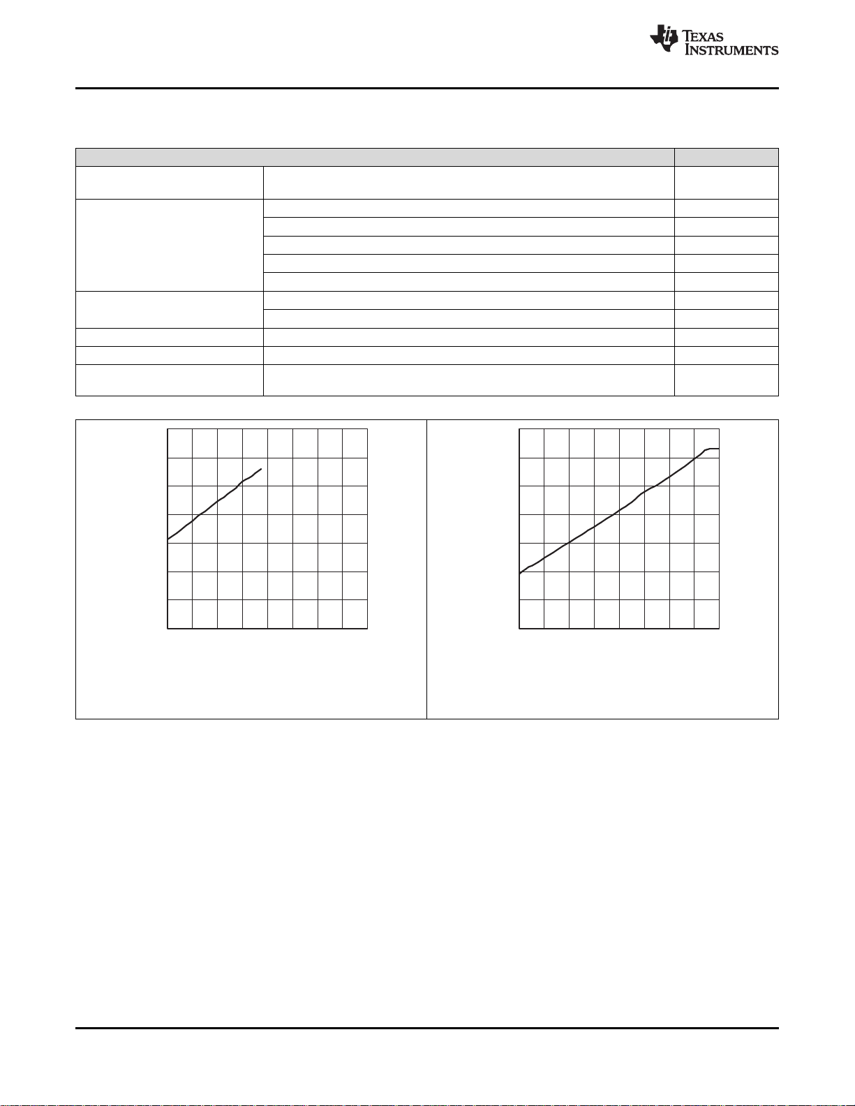
Table 1. Table Of Graphs
DC/DC CONVERTER FIGURE
Maximum output current vs Input voltage
vs Output current (TPS61030) (VO= 2.5 V, VI= 1.8 V, VSYNC = 0 V) Figure 3
vs Output current (TPS61031) (VO= 3.3 V, VI= 1.8 V, 2.4 V, VSYNC = 0 V) Figure 4
Efficiency vs Output current (TPS61032) (VO= 5.0 V, VI= 2.4 V, 3.3 V, VSYNC = 0 V) Figure 5
vs Input voltage (TPS61031) (IO= 10 mA, 100 mA, 1000 mA, VSYNC = 0 V) Figure 6
vs Input voltage (TPS61032) (IO= 10 mA, 100 mA, 1000 mA, VSYNC = 0 V) Figure 7
Output voltage
vs Output current (TPS61031) (VI= 2.4 V) Figure 8
vs Output current (TPS61032) (VI= 3.3 V) Figure 9
No-load supply current into VBAT vs Input voltage (TPS61032) Figure 10
No-load supply current into VOUT vs Input voltage (TPS61032) Figure 11
Minimum Load Resistance at
Startup
vs Input voltage (TPS61032) Figure 12
Figure 1,
Figure 2
Figure 1. TPS61031 Maximum Output Current Figure 2. TPS61032 Maximum Output Current
6 Submit Documentation Feedback Copyright © 2002–2015, Texas Instruments Incorporated
vs Input Voltage vs Input Voltage
Product Folder Links: TPS61030 TPS61031 TPS61032
50
55
60
65
70
75
80
85
90
95
100
1.8 2.2 2.6 3 3.4 3.8 4.2 4.6 5
Efficiency
- %
VI- Input Voltage - V
IO= 100 mA
IO= 10 mA
IO= 1000 mA
3.2
3.25
3.3
3.35
3.4
1 10 100 1000 10000
- Output V
oltage
- V
IO- Output Current - mA
V
O
50
80
90
100
Efficiency
- %
VI- Input Voltage - V
IO= 10 mA
IO= 100 mA
1.8 2 2.6 2.8 32.2 2.4 3.2
60
IO= 1000 mA
70
0
10
20
30
40
50
60
70
80
90
100
1 10 100 1000 10000
V
BAT
= 3.3 V
V
BAT
= 2.4 V
Efficiency
- %
IO- Output Current - mA
0
10
20
30
40
50
60
70
80
90
100
1 10 100 1000 10000
Efficiency
- %
IO- Output Current - mA
0
10
20
30
40
50
60
70
80
90
100
1 10 100 1000 10000
V
BAT
= 2.4 V
V
BAT
= 1.8 V
Efficiency
- %
IO- Output Current - mA
www.ti.com
TPS61030,TPS61031,TPS61032
SLUS534G –SEPTEMBER 2002–REVISED MARCH 2015
VO= 2.5 V VI= 1.8 V
Figure 3. TPS61030 Efficiency vs Output Current
VO= 5 V
Figure 5. Tps61032 Efficiency vs Output Current
VO= 3.3 V
Figure 4. TPS61031 Efficiency vs Output Current
Figure 6. TPS61031 Efficiency vs Input Voltage
Figure 7. TPS61032 Efficiency vs Input Voltage Figure 8. TPS61031 Output Voltage vs Output Current
Copyright © 2002–2015, Texas Instruments Incorporated Submit Documentation Feedback 7
VBAT = 2.4 V
Product Folder Links: TPS61030 TPS61031 TPS61032
SW
C1
10 µF
Power
Supply
L1
6.8 µH
R1
R2
VBAT
VOUT
FB
C2
2.2 µFC3220 µF
LBO
PGND
LBI
SYNC
EN
GND
TPS6103x
V
CC
Boost Output
Control Output
R3
R4
R6
0
2
4
6
8
10
12
14
1.8 2.2 2.6 3 3.4 3.8 4.2 4.6 5
V
- Input Voltage - V
Minimum Load Resistance at Startup
-
Ω
0
2
4
6
8
10
12
14
2 3 4 5
VI- Input Voltage - V
–40 C°
85 C°
25 C°
µA
No-Load Supply Current Into VOUT
-
4.8
4.85
4.9
4.95
5
5.05
5.1
5.15
5.2
1 10 100 1000 10000
- Output V
oltage
- V
IO- Output Current - mA
V
O
0
2
4
6
8
10
12
14
16
2 3 4 5
VI- Input Voltage - V
–40 C°
85 C°
25 C°
µA
No-Load Supply Current Into VBA
T -
TPS61030,TPS61031,TPS61032
SLUS534G –SEPTEMBER 2002–REVISED MARCH 2015
VBAT = 3.3 V
www.ti.com
Figure 9. TPS61032 Output Voltage
vs Output Current
Figure 11. TPS61032 No-Load Supply Current Into Vout
vs Input Voltage
9 Parameter Measurement Information
Figure 10. TPS61032 No-Load Supply Current into Vbat
vs input Voltage
Figure 12. Minimum Load Resistance at Start-Up
vs Input Voltage
8 Submit Documentation Feedback Copyright © 2002–2015, Texas Instruments Incorporated
Product Folder Links: TPS61030 TPS61031 TPS61032
Anti-
Ringing
Gate
Control
PGND
Regulator
PGND
Control Logic
Oscillator
Temperature
Control
VOUT
PGND
FB
SW
VBAT
EN
SYNC
GND
LBI
LBO
_
+
100 kW
10 pF
_
+
V
REF
= 0.5 V
GND
Error Amplifier
_
+
_
+
GND
V
REF
= 0.5 V
Low Battery Comparator
TPS61030,TPS61031,TPS61032
www.ti.com
SLUS534G –SEPTEMBER 2002–REVISED MARCH 2015
10 Detailed Description
10.1 Overview
The TPS6103x synchronous step-up converter typically operates at a 600 kHz frequency pulse width modulation
(PWM) at moderate to heavy load currents. The converter enters Power Save mode at low load currents to
maintain a high efficiency over a wide load. The Power Save mode can also be disabled, forcing the converter to
operate at a fixed switching frequency. The TPS6103x family is based on a fixed frequency with multiple feed
forward controller topology. Input voltage, output voltage, and voltage drop on the NMOS switch are monitored
and forwarded to the regulator. The peak current of the NMOS switch is also sensed to limit the maximum
current flowing through the switch and the inductor. It can also operate synchronized to an external clock signal
that is applied to the SYNC pin. Additionally, TPS6103x integrated the low-battery detector circuit typically used
to supervise the battery voltage and to generate an error flag when the battery voltage drops below a user-set
threshold voltage.
10.2 Functional Block Diagram
Product Folder Links: TPS61030 TPS61031 TPS61032
Copyright © 2002–2015, Texas Instruments Incorporated Submit Documentation Feedback 9

TPS61030,TPS61031,TPS61032
SLUS534G –SEPTEMBER 2002–REVISED MARCH 2015
www.ti.com
10.3 Feature Description
10.3.1 Controller Circuit
The controller circuit of the device is based on a fixed frequency multiple feedforward controller topology. Input
voltage, output voltage, and voltage drop on the NMOS switch are monitored and forwarded to the regulator. So
changes in the operating conditions of the converter directly affect the duty cycle and must not take the indirect
and slow way through the control loop and the error amplifier. The control loop, determined by the error amplifier,
only has to handle small signal errors. The input for it is the feedback voltage on the FB pin or, at fixed output
voltage versions, the voltage on the internal resistor divider. It is compared with the internal reference voltage to
generate an accurate and stable output voltage.
The peak current of the NMOS switch is also sensed to limit the maximum current flowing through the switch and
the inductor. The typical peak current limit is set to 4000 mA. An internal temperature sensor prevents the device
from getting overheated in case of excessive power dissipation.
10.3.2 Synchronous Rectifier
The device integrates an N-channel and a P-channel MOSFET transistor to realize a synchronous rectifier.
Because the commonly used discrete Schottky rectifier is replaced with a low RDS(ON) PMOS switch, the power
conversion efficiency reaches 96%. To avoid ground shift due to the high currents in the NMOS switch, two
separate ground pins are used. The reference for all control functions is the GND pin. The source of the NMOS
switch is connected to PGND. Both grounds must be connected on the PCB at only one point close to the GND
pin. A special circuit is applied to disconnect the load from the input during shutdown of the converter. In
conventional synchronous rectifier circuits, the backgate diode of the high-side PMOS is forward biased in
shutdown and allows current flowing from the battery to the output. This device however uses a special circuit
which takes the cathode of the backgate diode of the high-side PMOS and disconnects it from the source when
the regulator is not enabled (EN = low).
The benefit of this feature for the system design engineer is that the battery is not depleted during shutdown of
the converter. No additional components have to be added to the design to make sure that the battery is
disconnected from the output of the converter.
10.4 Device Functional Modes
10.4.1 Device Enable
The device is put into operation when EN is set high. It is put into a shutdown mode when EN is set to GND. In
shutdown mode, the regulator stops switching, all internal control circuitry including the low-battery comparator is
switched off, and the load is isolated from the input (as described in the Synchronous Rectifier Section). This
also means that the output voltage can drop below the input voltage during shutdown. During start-up of the
converter, the duty cycle and the peak current are limited in order to avoid high peak currents drawn from the
battery.
10.4.1.1 Undervoltage Lockout
An undervoltage lockout function prevents device start-up if the supply voltage on VBAT is lower than
approximately 1.6 V. When in operation and the battery is being discharged, the device automatically enters the
shutdown mode if the voltage on VBAT drops below approximately 1.6 V. This undervoltage lockout function is
implemented in order to prevent the malfunctioning of the converter.
10.4.2 Softstart
When the device enables the internal start-up cycle starts with the first step, the precharge phase. During
precharge, the rectifying switch is turned on until the output capacitor is charged to a value close to the input
voltage. The rectifying switch current is limited in that phase. This also limits the output current under short-circuit
conditions at the output. After charging the output capacitor to the input voltage the device starts switching. Until
the output voltage is reached, the boost switch current limit is set to 40% of its nominal value to avoid high peak
currents at the battery during startup. When the output voltage is reached, the regulator takes control and the
switch current limit is set back to 100%.
10 Submit Documentation Feedback Copyright © 2002–2015, Texas Instruments Incorporated
Product Folder Links: TPS61030 TPS61031 TPS61032

TPS61030,TPS61031,TPS61032
www.ti.com
SLUS534G –SEPTEMBER 2002–REVISED MARCH 2015
Device Functional Modes (continued)
10.4.3 Power Save Mode And Synchronization
The SYNC pin can be used to select different operation modes. To enable power save, SYNC must be set low.
Power save mode is used to improve efficiency at light load. In power save mode the converter only operates
when the output voltage trips below a set threshold voltage. It ramps up the output voltage with one or several
pulses and goes again into power save mode once the output voltage exceeds the set threshold voltage. This
power save mode can be disabled by setting the SYNC to VBAT.
Applying an external clock with a duty cycle between 30% and 70% at the SYNC pin forces the converter to
operate at the applied clock frequency. The external frequency has to be in the range of about ±20% of the
nominal internal frequency. Detailed values are shown in the electrical characteristic section of the data sheet.
10.4.4 Low Battery Detector Circuit—LBI/LBO
The low-battery detector circuit is typically used to supervise the battery voltage and to generate an error flag
when the battery voltage drops below a user-set threshold voltage. The function is active only when the device is
enabled. When the device is disabled, the LBO pin is high-impedance. The switching threshold is 500 mV at LBI.
During normal operation, LBO stays at high impedance when the voltage, applied at LBI, is above the threshold.
It is active low when the voltage at LBI goes below 500 mV.
The battery voltage, at which the detection circuit switches, can be programmed with a resistive divider
connected to the LBI pin. The resistive divider scales down the battery voltage to a voltage level of 500 mV,
which is then compared to the LBI threshold voltage. The LBI pin has a built-in hysteresis of 10 mV. See the
application section for more details about the programming of the LBI threshold. If the low-battery detection
circuit is not used, the LBI pin should be connected to GND (or to VBAT) and the LBO pin can be left
unconnected. Do not let the LBI pin float.
10.4.5 Low-EMI Switch
The device integrates a circuit that removes the ringing that typically appears on the SW node when the
converter enters discontinuous current mode. In this case, the current through the inductor ramps to zero and the
rectifying PMOS switch is turned off to prevent a reverse current flowing from the output capacitors back to the
battery. Due to the remaining energy that is stored in parasitic components of the semiconductor and the
inductor, a ringing on the SW pin is induced. The integrated antiringing switch clamps this voltage to VBAT and
therefore dampens ringing.
Copyright © 2002–2015, Texas Instruments Incorporated Submit Documentation Feedback 11
Product Folder Links: TPS61030 TPS61031 TPS61032

SW
C1Power
L1
R1
R2
VBAT
VOUT
FB
C2 C3
LBO
PGND
LBI
SYNC
EN
GND
TPS6103x
V
CC
Boost Output
Control Output
R3
R4
R6
TPS61030,TPS61031,TPS61032
SLUS534G –SEPTEMBER 2002–REVISED MARCH 2015
www.ti.com
11 Application and Implementation
NOTE
Information in the following applications sections is not part of the TI component
specification, and TI does not warrant its accuracy or completeness. TI’s customers are
responsible for determining suitability of components for their purposes. Customers should
validate and test their design implementation to confirm system functionality.
11.1 Application Information
The TPS6103x dc/dc converters are intended for systems powered by a dual or triple cell NiCd or NiMH battery
with a typical terminal voltage between 1.8 V and 5.5 V. They can also be used in systems powered by one-cell
Li-Ion with a typical stack voltage between 2.5 V and 4.2 V. Additionally, two or three primary and secondary
alkaline battery cells can be the power source in systems where the TPS6103x is used.
11.2 Typical Application
Figure 13. Typical Application Circuit For Adjustable Output Voltage Option
11.2.1 Design Requirements
Use the following typical application design procedure to select external components values for the TPS61030
device.
Table 2. TPS61030 5 V Output Design Parameters
DESIGN PARAMETERS EXAMPLE VALUES
Input Voltage Range 1.8 V to 5.5 V
Output Voltage 5.0 V
Output Voltage Ripple +/- 3% V
Transient Response +/- 10% V
Input Voltage Ripple +/- 200mV
Output Current 2A
Operating Frequency 600 kHz
12 Submit Documentation Feedback Copyright © 2002–2015, Texas Instruments Incorporated
Product Folder Links: TPS61030 TPS61031 TPS61032
OUT
OUT

L
+ I
OUT
V
OUT
V
BAT
0.8
ǒ
V
BAT
V
LBI*threshold
* 1Ǔ+ 390 kW
ǒ
V
BAT
500 mV
* 1
Ǔ
C
parR3
+ 10 pF
ǒ
200 kW
R4
–1
Ǔ
ǒ
V
O
V
FB
* 1Ǔ+ 180 kW
ǒ
V
O
500 mV
* 1
Ǔ
TPS61030,TPS61031,TPS61032
www.ti.com
11.2.2 Detailed Design Procedure
11.2.2.1 Programming The Output Voltage
The output voltage of the TPS61030 dc/dc converter section can be adjusted with an external resistor divider.
The typical value of the voltage on the FB pin is 500 mV. The maximum allowed value for the output voltage is
5.5 V. The current through the resistive divider should be about 100 times greater than the current into the FB
pin. The typical current into the FB pin is 0.01 µA, and the voltage across R6 is typically 500 mV. Based on those
two values, the recommended value for R4 should be lower than 500 kΩ, in order to set the divider current at 1
µA or higher. Because of internal compensation circuitry the value for this resistor should be in the range of 200
kΩ. From that, the value of resistor R3, depending on the needed output voltage (VO), can be calculated using
equation 1:
If as an example, an output voltage of 3.3 V is needed, a 1-MΩ resistor should be chosen for R3. If for any
reason the value for R4 is chosen significantly lower than 200 kΩ additional capacitance in parallel to R3 is
recommended. The required capacitance value can be easily calculated using Equation 2:
11.2.2.2 Programming The LBI/LBO Threshold Voltage
The current through the resistive divider should be about 100 times greater than the current into the LBI pin. The
typical current into the LBI pin is 0.01 µA, and the voltage across R2 is equal to the LBI voltage threshold that is
generated on-chip, which has a value of 500 mV. The recommended value for R2 is therefore in the range of 500
kΩ. From that, the value of resistor R1, depending on the desired minimum battery voltage V
calculated using Equation 3.
SLUS534G –SEPTEMBER 2002–REVISED MARCH 2015
(1)
(2)
can be
BAT,
(3)
The output of the low battery supervisor is a simple open-drain output that goes active low if the dedicated
battery voltage drops below the programmed threshold voltage on LBI. The output requires a pullup resistor with
a recommended value of 1 MΩ. The maximum voltage which is used to pull up the LBO outputs should not
exceed the output voltage of the dc/dc converter. If not used, the LBO pin can be left floating or tied to GND.
11.2.2.3 Inductor Selection
A boost converter normally requires two main passive components for storing energy during the conversion. A
boost inductor and a storage capacitor at the output are required. To select the boost inductor, it is
recommended to keep the possible peak inductor current below the current limit threshold of the power switch in
the chosen configuration. For example, the current limit threshold of the TPS6103x's switch is 4500 mA at an
output voltage of 5 V. The highest peak current through the inductor and the switch depends on the output load,
the input (V
using Equation 4:
For example, for an output current of 1000 mA at 5 V, at least 3500 mA of average current flows through the
inductor at a minimum input voltage of 1.8 V.
The second parameter for choosing the inductor is the desired current ripple in the inductor. Normally, it is
advisable to work with a ripple of less than 20% of the average inductor current. A smaller ripple reduces the
magnetic hysteresis losses in the inductor, as well as output voltage ripple and EMI. But in the same way,
regulation time at load changes rises. In addition, a larger inductor increases the total system costs. With those
parameters, it is possible to calculate the value for the inductor by using Equation 5:
), and the output voltage (V
BAT
). Estimation of the maximum average inductor current can be done
OUT
(4)
Copyright © 2002–2015, Texas Instruments Incorporated Submit Documentation Feedback 13
Product Folder Links: TPS61030 TPS61031 TPS61032

ESR
+ I
OUT
R
ESR
min
+
I
OUT
ǒ
V
OUT
* V
BAT
Ǔ
ƒ DV V
OUT
V
BAT
ǒ
V
OUT–VBAT
Ǔ
DIL ƒ V
OUT
TPS61030,TPS61031,TPS61032
SLUS534G –SEPTEMBER 2002–REVISED MARCH 2015
www.ti.com
(5)
Parameter f is the switching frequency and ΔILis the ripple current in the inductor, i.e., 10% × IL. In this example,
the desired inductor has the value of 5.5 µH. In typical applications a 6.8 µH inductance is recommended. The
minimum possible inductance value is 2.2 µH. With the calculated inductance and current values, it is possible to
choose a suitable inductor. Care has to be taken that load transients and losses in the circuit can lead to higher
currents as estimated in equation 4. Also, the losses in the inductor caused by magnetic hysteresis losses and
copper losses are a major parameter for total circuit efficiency.
The following inductor series from different suppliers have been used with the TPS6103x converters:
Table 3. List Of Inductors
VENDOR INDUCTOR SERIES
CDRH124
Sumida CDRH103R
CDRH104R
Wurth Electronik
EPCOS B82464G
(1) See Third-Party Products Disclaimer
7447779___
744771___
(1)
11.2.2.4 Capacitor Selection
11.2.2.4.1 Input Capacitor
At least a 10-µF input capacitor is recommended to improve transient behavior of the regulator and EMI behavior
of the total power supply circuit. A ceramic capacitor or a tantalum capacitor with a 100-nF ceramic capacitor in
parallel, placed close to the IC, is recommended.
11.2.2.4.2 Output Capacitor
The major parameter necessary to define the output capacitor is the maximum allowed output voltage ripple of
the converter. This ripple is determined by two parameters of the capacitor, the capacitance and the ESR. It is
possible to calculate the minimum capacitance needed for the defined ripple, supposing that the ESR is zero, by
using Equation 6:
(6)
Parameter f is the switching frequency and ΔV is the maximum allowed ripple.
With a chosen ripple voltage of 10 mV, a minimum capacitance of 100 µF is needed. The total ripple is larger
due to the ESR of the output capacitor. This additional component of the ripple can be calculated using
Equation 7:
(7)
An additional ripple of 80 mV is the result of using a tantalum capacitor with a low ESR of 80 mΩ. The total ripple
is the sum of the ripple caused by the capacitance and the ripple caused by the ESR of the capacitor. In this
example, the total ripple is 90 mV. Additional ripple is caused by load transients. This means that the output
capacitance needs to be larger than calculated above to meet the total ripple requirements.
The output capacitor must completely supply the load during the charging phase of the inductor. A reasonable
value of the output capacitance depends on the speed of the load transients and the load current during the load
change. With the calculated minimum value of 100 µF and load transient considerations, a recommended output
capacitance value is in around 220 µF. For economical reasons this usually is a tantalum capacitor. Because of
this the control loop has been optimized for using output capacitors with an ESR of above 30 mΩ. The minimum
value for the output capacitor is 22 µF.
14 Submit Documentation Feedback Copyright © 2002–2015, Texas Instruments Incorporated
Product Folder Links: TPS61030 TPS61031 TPS61032

Output Voltage
20 mV/Div, AC
Input Voltage
500 mV/Div, DC
Timebase - 2 ms/Div
Output Voltage
50 mV/Div, AC
Output Current
500 mA/Div, DC
Timebase - 2 ms/Div
Inductor Current
200 mA/Div, DC
Output Voltage
50 mV/Div, AC
Timebase - 200 ms/Div
Inductor Current
200 mA/Div
Output Voltage
20 mV/Div
Timebase - 1 ms/Div
A
REG
+
d
V
FB
+
5 (R3) R4)
R4 (1) i w 2.3 ms)
TPS61030,TPS61031,TPS61032
www.ti.com
11.2.2.4.2.1 Small Signal Stability
SLUS534G –SEPTEMBER 2002–REVISED MARCH 2015
When using output capacitors with lower ESR, like ceramics, it is recommended to use the adjustable voltage
version. The missing ESR can be easily compensated there in the feedback divider. Typically a capacitor in the
range of 10 pF in parallel to R3 helps to obtain small signal stability with lowest ESR output capacitors. For more
detailed analysis the small signal transfer function of the error amplifier and regulator, which is given in Equation
8, can be used.
(8)
11.2.3 Application Curves
VI= 3.3 V RL= 5 Ω
Figure 14. TPS61030 Output Voltage in Continuous Mode
VI= 2.5 V IL= 80 mA to 800 mA
Figure 16. TPS61030 Load Transient Response
VI= 3.3 V RL= 100 Ω
Figure 15. TPS61030 Output Voltage in Power Save Mode
VI= 2.2 V to 2.7 V RL= 50 Ω
Figure 17. TPS61030 Line Transient Response
Copyright © 2002–2015, Texas Instruments Incorporated Submit Documentation Feedback 15
Product Folder Links: TPS61030 TPS61031 TPS61032

SW
C1
10 µF
L1
6.8 µH
R1
R2
VBAT
VOUT
FB
C2
2.2 µFC3220 µF
LBO
PGND
LBI
SYNC
EN
GND
TPS61032
VCC 5 V
Boost Output
LBO
R6
Battery
Input
Output Voltage
2 V/Div, DC
Input Current
500 mA/Div, DC
Enable
5 V/Div, DC
Voltage at SW
2 V/Div, DC
Timebase - 400 ms/Div
TPS61030,TPS61031,TPS61032
SLUS534G –SEPTEMBER 2002–REVISED MARCH 2015
VI= 2.4 V RL= 20 Ω
Figure 18. TPS61030 DC/DC Converter Start-Up After Enable
11.2.4 System Examples
11.2.4.1 Power Supply Solution For Maximum Output Power
Second application example
www.ti.com
Figure 19. Power Supply Solution For Maximum Output Power
16 Submit Documentation Feedback Copyright © 2002–2015, Texas Instruments Incorporated
Product Folder Links: TPS61030 TPS61031 TPS61032

SW
C1
10 µF
L1
6.8 µH
R1
R2
VBAT
VOUT
R6
C2
2.2 µFC3220 µF
LBO
PGND
LBI
SYNC
EN
GND
TPS61032
LBO
C5
0.1 µF
DS1
C6
1 µF
V
CC2
–5 V
Unregulated
Auxiliary Output
Battery
Input
FB
V
CC1
5 V
Boost Main Output
SW
C3
10 µF
L1
6.8 µH
R1
R2
VBAT
VOUT
R6
C2
2.2 µFC3220 µF
LBO
PGND
LBI
SYNC
EN
GND
TPS61032
LBO
C5
0.1 µF
DS1
C6
1 µF
V
CC2
10 V
Unregulated
Auxiliary Output
Battery
Input
FB
V
CC1
5 V
Boost Main Output
www.ti.com
SLUS534G –SEPTEMBER 2002–REVISED MARCH 2015
11.2.4.2 Power Supply Solution With Auxiliary Positive Output Voltage
Third application example
TPS61030,TPS61031,TPS61032
Figure 20. Power Supply Solution With Auxiliary Positive Output Voltage
11.2.4.3 Power Supply Solution with Auxiliary Negative Output Voltage
Fourth application example
Copyright © 2002–2015, Texas Instruments Incorporated Submit Documentation Feedback 17
Figure 21. Power Supply Solution With Auxiliary Negative Output Voltage
Product Folder Links: TPS61030 TPS61031 TPS61032

VIA to Ground Plane
Feedback
Resistor 1
Inductor
Output
Capacitor 1
VOUT
Exposed PAD
FB
GND
PGND
VBAT
VOUT
SW
NC
PGND
PGND
LBO
SW
VOUT
EN
SYNC
LBI
LBO Resistor
GND
VIA to VBAT Plane
Input
Capacitor
GND
LBI
Resistor 1
LBI
Resistor 2
Feedback
Resistor 2
Output
Capacitor 2
TPS61030,TPS61031,TPS61032
SLUS534G –SEPTEMBER 2002–REVISED MARCH 2015
www.ti.com
12 Power Supply Recommendations
The device is designed to operate from an input voltage supply range between 1.8 V and 5.5 V. This input supply
must be well regulated. If the input supply is located more than a few inches from the converter, additional bulk
capacitance may be required in addition to the ceramic bypass capacitors. An electrolytic or tantalum capacitor
with a value of 47 μF is a typical choice.
13 Layout
13.1 Layout Considerations
As for all switching power supplies, the layout is an important step in the design, especially at high peak currents
and high switching frequencies. If the layout is not carefully done, the regulator could show stability problems as
well as EMI problems. Therefore, use wide and short traces for the main current path and for the power ground
tracks. The input capacitor, output capacitor, and the inductor should be placed as close as possible to the IC.
Use a common ground node for power ground and a different one for control ground to minimize the effects of
ground noise. Connect these ground nodes at any place close to one of the ground pins of the IC.
The feedback divider should be placed as close as possible to the control ground pin of the IC. To lay out the
control ground, it is recommended to use short traces as well, separated from the power ground traces. This
avoids ground shift problems, which can occur due to superimposition of power ground current and control
ground current.
13.2 Layout Example
13.3 Thermal Considerations
Implementation of integrated circuits in low-profile and fine-pitch surface-mount packages typically requires
special attention to power dissipation. Many system-dependent issues such as thermal coupling, airflow, added
heat sinks and convection surfaces, and the presence of other heat-generating components affect the powerdissipation limits of a given component.
18 Submit Documentation Feedback Copyright © 2002–2015, Texas Instruments Incorporated
Product Folder Links: TPS61030 TPS61031 TPS61032

P
D(MAX)
+
T
J(MAX)
* T
A
R
qJA
+
125°C * 85°C
36.5°CńW
TPS61030,TPS61031,TPS61032
www.ti.com
SLUS534G –SEPTEMBER 2002–REVISED MARCH 2015
Thermal Considerations (continued)
Three basic approaches for enhancing thermal performance are listed below:
• Improving the power dissipation capability of the PCB design
• Improving the thermal coupling of the component to the PCB
• Introducing airflow in the system
The maximum junction temperature (TJ) of the TPS6103x devices is 125°C. The thermal resistance of the 16-pin
TSSOP PowerPAD package (PWP) is R
= 36.5°C/W (QFN package, RSA, 38.1°C/W), if the PowerPAD is
ΘJA
soldered. Specified regulator operation is assured to a maximum ambient temperature TAof 85°C. Therefore, the
maximum power dissipation for the PWP package is about 1096 mW, for the RSA package it is about 1050 mW.
More power can be dissipated if the maximum ambient temperature of the application is lower.
(9)
14 Device and Documentation Support
14.1 Device Support
14.1.1 Third-Party Products Disclaimer
TI'S PUBLICATION OF INFORMATION REGARDING THIRD-PARTY PRODUCTS OR SERVICES DOES NOT
CONSTITUTE AN ENDORSEMENT REGARDING THE SUITABILITY OF SUCH PRODUCTS OR SERVICES
OR A WARRANTY, REPRESENTATION OR ENDORSEMENT OF SUCH PRODUCTS OR SERVICES, EITHER
ALONE OR IN COMBINATION WITH ANY TI PRODUCT OR SERVICE.
14.2 Related Links
The table below lists quick access links. Categories include technical documents, support and community
resources, tools and software, and quick access to sample or buy.
Table 4. Related Links
PARTS PRODUCT FOLDER SAMPLE & BUY
TPS61030 Click here Click here Click here Click here Click here
TPS61031 Click here Click here Click here Click here Click here
TPS61032 Click here Click here Click here Click here Click here
TECHNICAL TOOLS & SUPPORT &
DOCUMENTS SOFTWARE COMMUNITY
14.3 Trademarks
PowerPAD is a trademark of Texas Instruments.
All other trademarks are the property of their respective owners.
14.4 Electrostatic Discharge Caution
These devices have limited built-in ESD protection. The leads should be shorted together or the device placed in conductive foam
during storage or handling to prevent electrostatic damage to the MOS gates.
14.5 Glossary
SLYZ022 — TI Glossary.
This glossary lists and explains terms, acronyms, and definitions.
15 Mechanical, Packaging, and Orderable Information
The following pages include mechanical, packaging, and orderable information. This information is the most
current data available for the designated devices. This data is subject to change without notice and revision of
this document. For browser-based versions of this data sheet, refer to the left-hand navigation.
Copyright © 2002–2015, Texas Instruments Incorporated Submit Documentation Feedback 19
Product Folder Links: TPS61030 TPS61031 TPS61032

PACKAGE OPTION ADDENDUM
www.ti.com
PACKAGING INFORMATION
Orderable Device Status
TPS61030PWP ACTIVE HTSSOP PWP 16 90 Green (RoHS
TPS61030PWPG4 ACTIVE HTSSOP PWP 16 90 Green (RoHS
TPS61030PWPR ACTIVE HTSSOP PWP 16 2000 Green (RoHS
TPS61030PWPRG4 ACTIVE HTSSOP PWP 16 2000 Green (RoHS
TPS61030RSAR ACTIVE QFN RSA 16 3000 Green (RoHS
TPS61030RSARG4 ACTIVE QFN RSA 16 3000 Green (RoHS
TPS61031PWP ACTIVE HTSSOP PWP 16 90 Green (RoHS
TPS61031PWPG4 ACTIVE HTSSOP PWP 16 90 Green (RoHS
TPS61031PWPR ACTIVE HTSSOP PWP 16 2000 Green (RoHS
TPS61031PWPRG4 ACTIVE HTSSOP PWP 16 2000 Green (RoHS
TPS61031RSAR ACTIVE QFN RSA 16 3000 Green (RoHS
TPS61032PWP ACTIVE HTSSOP PWP 16 90 Green (RoHS
TPS61032PWPG4 ACTIVE HTSSOP PWP 16 90 Green (RoHS
TPS61032PWPR ACTIVE HTSSOP PWP 16 2000 Green (RoHS
TPS61032PWPRG4 ACTIVE HTSSOP PWP 16 TBD Call TI Call TI -40 to 85
Package Type Package
(1)
Drawing
Pins Package
Qty
Eco Plan
(2)
& no Sb/Br)
& no Sb/Br)
& no Sb/Br)
& no Sb/Br)
& no Sb/Br)
& no Sb/Br)
& no Sb/Br)
& no Sb/Br)
& no Sb/Br)
& no Sb/Br)
& no Sb/Br)
& no Sb/Br)
& no Sb/Br)
& no Sb/Br)
Lead/Ball Finish
(6)
MSL Peak Temp
(3)
CU NIPDAU Level-2-260C-1 YEAR -40 to 85 PS61030
CU NIPDAU Level-2-260C-1 YEAR -40 to 85 PS61030
CU NIPDAU Level-2-260C-1 YEAR -40 to 85 PS61030
CU NIPDAU Level-2-260C-1 YEAR -40 to 85 PS61030
CU NIPDAU Level-2-260C-1 YEAR -40 to 85 TPS6
CU NIPDAU Level-2-260C-1 YEAR -40 to 85 TPS6
CU NIPDAU Level-2-260C-1 YEAR -40 to 85 PS61031
CU NIPDAU Level-2-260C-1 YEAR -40 to 85 PS61031
CU NIPDAU Level-2-260C-1 YEAR -40 to 85 PS61031
CU NIPDAU Level-2-260C-1 YEAR -40 to 85 PS61031
CU NIPDAU Level-2-260C-1 YEAR -40 to 85 TPS6
CU NIPDAU Level-2-260C-1 YEAR -40 to 85 PS61032
CU NIPDAU Level-2-260C-1 YEAR -40 to 85 PS61032
CU NIPDAU Level-2-260C-1 YEAR -40 to 85 PS61032
10-Mar-2015
Op Temp (°C) Device Marking
(4/5)
1030
1030
1031
Samples
TPS61032RSAR ACTIVE QFN RSA 16 3000 Green (RoHS
TPS61032RSARG4 ACTIVE QFN RSA 16 3000 Green (RoHS
& no Sb/Br)
& no Sb/Br)
Addendum-Page 1
CU NIPDAU Level-2-260C-1 YEAR -40 to 85 TPS6
1032
CU NIPDAU Level-2-260C-1 YEAR -40 to 85 TPS6
1032

PACKAGE OPTION ADDENDUM
www.ti.com
(1)
The marketing status values are defined as follows:
ACTIVE: Product device recommended for new designs.
LIFEBUY: TI has announced that the device will be discontinued, and a lifetime-buy period is in effect.
NRND: Not recommended for new designs. Device is in production to support existing customers, but TI does not recommend using this part in a new design.
PREVIEW: Device has been announced but is not in production. Samples may or may not be available.
OBSOLETE: TI has discontinued the production of the device.
10-Mar-2015
(2)
Eco Plan - The planned eco-friendly classification: Pb-Free (RoHS), Pb-Free (RoHS Exempt), or Green (RoHS & no Sb/Br) - please check http://www.ti.com/productcontent for the latest availability
information and additional product content details.
TBD: The Pb-Free/Green conversion plan has not been defined.
Pb-Free (RoHS): TI's terms "Lead-Free" or "Pb-Free" mean semiconductor products that are compatible with the current RoHS requirements for all 6 substances, including the requirement that
lead not exceed 0.1% by weight in homogeneous materials. Where designed to be soldered at high temperatures, TI Pb-Free products are suitable for use in specified lead-free processes.
Pb-Free (RoHS Exempt): This component has a RoHS exemption for either 1) lead-based flip-chip solder bumps used between the die and package, or 2) lead-based die adhesive used between
the die and leadframe. The component is otherwise considered Pb-Free (RoHS compatible) as defined above.
Green (RoHS & no Sb/Br): TI defines "Green" to mean Pb-Free (RoHS compatible), and free of Bromine (Br) and Antimony (Sb) based flame retardants (Br or Sb do not exceed 0.1% by weight
in homogeneous material)
(3)
MSL, Peak Temp. - The Moisture Sensitivity Level rating according to the JEDEC industry standard classifications, and peak solder temperature.
(4)
There may be additional marking, which relates to the logo, the lot trace code information, or the environmental category on the device.
(5)
Multiple Device Markings will be inside parentheses. Only one Device Marking contained in parentheses and separated by a "~" will appear on a device. If a line is indented then it is a continuation
of the previous line and the two combined represent the entire Device Marking for that device.
(6)
Lead/Ball Finish - Orderable Devices may have multiple material finish options. Finish options are separated by a vertical ruled line. Lead/Ball Finish values may wrap to two lines if the finish
value exceeds the maximum column width.
Important Information and Disclaimer:The information provided on this page represents TI's knowledge and belief as of the date that it is provided. TI bases its knowledge and belief on information
provided by third parties, and makes no representation or warranty as to the accuracy of such information. Efforts are underway to better integrate information from third parties. TI has taken and
continues to take reasonable steps to provide representative and accurate information but may not have conducted destructive testing or chemical analysis on incoming materials and chemicals.
TI and TI suppliers consider certain information to be proprietary, and thus CAS numbers and other limited information may not be available for release.
In no event shall TI's liability arising out of such information exceed the total purchase price of the TI part(s) at issue in this document sold by TI to Customer on an annual basis.
Addendum-Page 2

PACKAGE MATERIALS INFORMATION
www.ti.com 13-Feb-2016
TAPE AND REEL INFORMATION
*All dimensions are nominal
Device Package
Type
TPS61030PWPR HTSSOP PWP 16 2000 330.0 12.4 6.9 5.6 1.6 8.0 12.0 Q1
TPS61030RSAR QFN RSA 16 3000 330.0 12.4 4.3 4.3 1.5 8.0 12.0 Q2
TPS61031PWPR HTSSOP PWP 16 2000 330.0 12.4 6.9 5.6 1.6 8.0 12.0 Q1
TPS61031RSAR QFN RSA 16 3000 330.0 12.4 4.3 4.3 1.5 8.0 12.0 Q2
TPS61032PWPR HTSSOP PWP 16 2000 330.0 12.4 6.9 5.6 1.6 8.0 12.0 Q1
TPS61032RSAR QFN RSA 16 3000 330.0 12.4 4.3 4.3 1.5 8.0 12.0 Q2
Package
Drawing
Pins SPQ Reel
Diameter
(mm)
Reel
Width
W1 (mm)
A0
(mm)B0(mm)K0(mm)P1(mm)W(mm)
Pin1
Quadrant
Pack Materials-Page 1

PACKAGE MATERIALS INFORMATION
www.ti.com 13-Feb-2016
*All dimensions are nominal
Device Package Type Package Drawing Pins SPQ Length (mm) Width (mm) Height (mm)
TPS61030PWPR HTSSOP PWP 16 2000 367.0 367.0 38.0
TPS61030RSAR QFN RSA 16 3000 338.1 338.1 20.6
TPS61031PWPR HTSSOP PWP 16 2000 367.0 367.0 38.0
TPS61031RSAR QFN RSA 16 3000 338.1 338.1 20.6
TPS61032PWPR HTSSOP PWP 16 2000 367.0 367.0 38.0
TPS61032RSAR QFN RSA 16 3000 338.1 338.1 20.6
Pack Materials-Page 2


IMPORTANT NOTICE
Texas Instruments Incorporated and its subsidiaries (TI) reserve the right to make corrections, enhancements, improvements and other
changes to its semiconductor products and services per JESD46, latest issue, and to discontinue any product or service per JESD48, latest
issue. Buyers should obtain the latest relevant information before placing orders and should verify that such information is current and
complete. All semiconductor products (also referred to herein as “components”) are sold subject to TI’s terms and conditions of sale
supplied at the time of order acknowledgment.
TI warrants performance of its components to the specifications applicable at the time of sale, in accordance with the warranty in TI’s terms
and conditions of sale of semiconductor products. Testing and other quality control techniques are used to the extent TI deems necessary
to support this warranty. Except where mandated by applicable law, testing of all parameters of each component is not necessarily
performed.
TI assumes no liability for applications assistance or the design of Buyers’ products. Buyers are responsible for their products and
applications using TI components. To minimize the risks associated with Buyers’ products and applications, Buyers should provide
adequate design and operating safeguards.
TI does not warrant or represent that any license, either express or implied, is granted under any patent right, copyright, mask work right, or
other intellectual property right relating to any combination, machine, or process in which TI components or services are used. Information
published by TI regarding third-party products or services does not constitute a license to use such products or services or a warranty or
endorsement thereof. Use of such information may require a license from a third party under the patents or other intellectual property of the
third party, or a license from TI under the patents or other intellectual property of TI.
Reproduction of significant portions of TI information in TI data books or data sheets is permissible only if reproduction is without alteration
and is accompanied by all associated warranties, conditions, limitations, and notices. TI is not responsible or liable for such altered
documentation. Information of third parties may be subject to additional restrictions.
Resale of TI components or services with statements different from or beyond the parameters stated by TI for that component or service
voids all express and any implied warranties for the associated TI component or service and is an unfair and deceptive business practice.
TI is not responsible or liable for any such statements.
Buyer acknowledges and agrees that it is solely responsible for compliance with all legal, regulatory and safety-related requirements
concerning its products, and any use of TI components in its applications, notwithstanding any applications-related information or support
that may be provided by TI. Buyer represents and agrees that it has all the necessary expertise to create and implement safeguards which
anticipate dangerous consequences of failures, monitor failures and their consequences, lessen the likelihood of failures that might cause
harm and take appropriate remedial actions. Buyer will fully indemnify TI and its representatives against any damages arising out of the use
of any TI components in safety-critical applications.
In some cases, TI components may be promoted specifically to facilitate safety-related applications. With such components, TI’s goal is to
help enable customers to design and create their own end-product solutions that meet applicable functional safety standards and
requirements. Nonetheless, such components are subject to these terms.
No TI components are authorized for use in FDA Class III (or similar life-critical medical equipment) unless authorized officers of the parties
have executed a special agreement specifically governing such use.
Only those TI components which TI has specifically designated as military grade or “enhanced plastic” are designed and intended for use in
military/aerospace applications or environments. Buyer acknowledges and agrees that any military or aerospace use of TI components
which have not been so designated is solely at the Buyer's risk, and that Buyer is solely responsible for compliance with all legal and
regulatory requirements in connection with such use.
TI has specifically designated certain components as meeting ISO/TS16949 requirements, mainly for automotive use. In any case of use of
non-designated products, TI will not be responsible for any failure to meet ISO/TS16949.
Products Applications
Audio www.ti.com/audio Automotive and Transportation www.ti.com/automotive
Amplifiers amplifier.ti.com Communications and Telecom www.ti.com/communications
Data Converters dataconverter.ti.com Computers and Peripherals www.ti.com/computers
DLP® Products www.dlp.com Consumer Electronics www.ti.com/consumer-apps
DSP dsp.ti.com Energy and Lighting www.ti.com/energy
Clocks and Timers www.ti.com/clocks Industrial www.ti.com/industrial
Interface interface.ti.com Medical www.ti.com/medical
Logic logic.ti.com Security www.ti.com/security
Power Mgmt power.ti.com Space, Avionics and Defense www.ti.com/space-avionics-defense
Microcontrollers microcontroller.ti.com Video and Imaging www.ti.com/video
RFID www.ti-rfid.com
OMAP Applications Processors www.ti.com/omap TI E2E Community e2e.ti.com
Wireless Connectivity www.ti.com/wirelessconnectivity
Mailing Address: Texas Instruments, Post Office Box 655303, Dallas, Texas 75265
Copyright © 2016, Texas Instruments Incorporated

 Loading...