

Texas Instruments TPS60141PWPR, TPS60141PWP, TPS60140PWPR, TPS60140PWP, TPS60140EVM-144 Datasheet
TPS60140, TPS60141
LOW POWER DC-DC CONVERTER
REGULATED 5 V, 100-mA CHARGE PUMP VOLTAGE TRIPLER
SLVS273– FEBRUAR Y 2000
1
POST OFFICE BOX 655303 • DALLAS, TEXAS 75265
features
D
Regulated 5 V ± 4% Output Voltage With up
to 100 mA Output Current From a 1.8 V to
3.6 V Input Voltage Range
D
65-µA Quiescent Supply Current
D
0.05-µA Shutdown Current, Battery Is
Isolated From Load in Shutdown
D
Integrated Low-Battery or Power-Good
Indicator
D
Low Output Voltage Ripple Over Complete
Output Current Range
D
Easy-To-Design With Low-EMI Power
Supply Since no Inductors Are Required
D
Evaluation Module Available
(TPS60140EVM-144)
applications
D
Replaces DC/DC Converters With Inductors
in Battery-Powered Applications:
– Two Battery Cells to 5 V Conversion
– Portable Instruments
– Miniature Equipment
– Backup-Battery Boost Converters
– Medical Instruments
– 5-V Smart Card Supply
– Organizers, PDAs
·
description
The TPS6014x step-up, regulated charge pumps
generate a 5-V ±4% output voltage from a 1.8 V
to 3.6 V input voltage range. The devices are
typically powered by two alkaline, NiCd, or NiMH
battery cells and provide an output current of
minimum 100 mA from a 2-V input. Only four
external capacitors are needed to build a
complete voltage tripler charge pump.
The devices regulate the output by using the
pulse-skip topology . The controller is optimized for
lowest output voltage ripple over the complete output current range. The output peak current and therefore the
output voltage ripple are drastically reduced compared to a conventional pulse-skip topology by regulating the
charge pump output resistance. At light loads the maximum output resistance is limited to assure a low
quiescent current.
The TPS60140 includes a low-battery comparator that issues a warning if the battery voltage drops below a
user-adjustable threshold voltage. The TPS60141 features a power-good output that goes active when the
output voltage reaches 90% of its nominal value.
The logic shutdown function disables the converter, reduces the supply current to a maximum of 1 µA and
disconnects the output from the input. Special current-control circuitry prevents excessive current from being
drawn from the battery during start-up. This dc-dc converter requires no inductors, therefore, EMI is of little
concern. It is available in the small, thermally enhanced 20-pin TSSOP package (PWP).
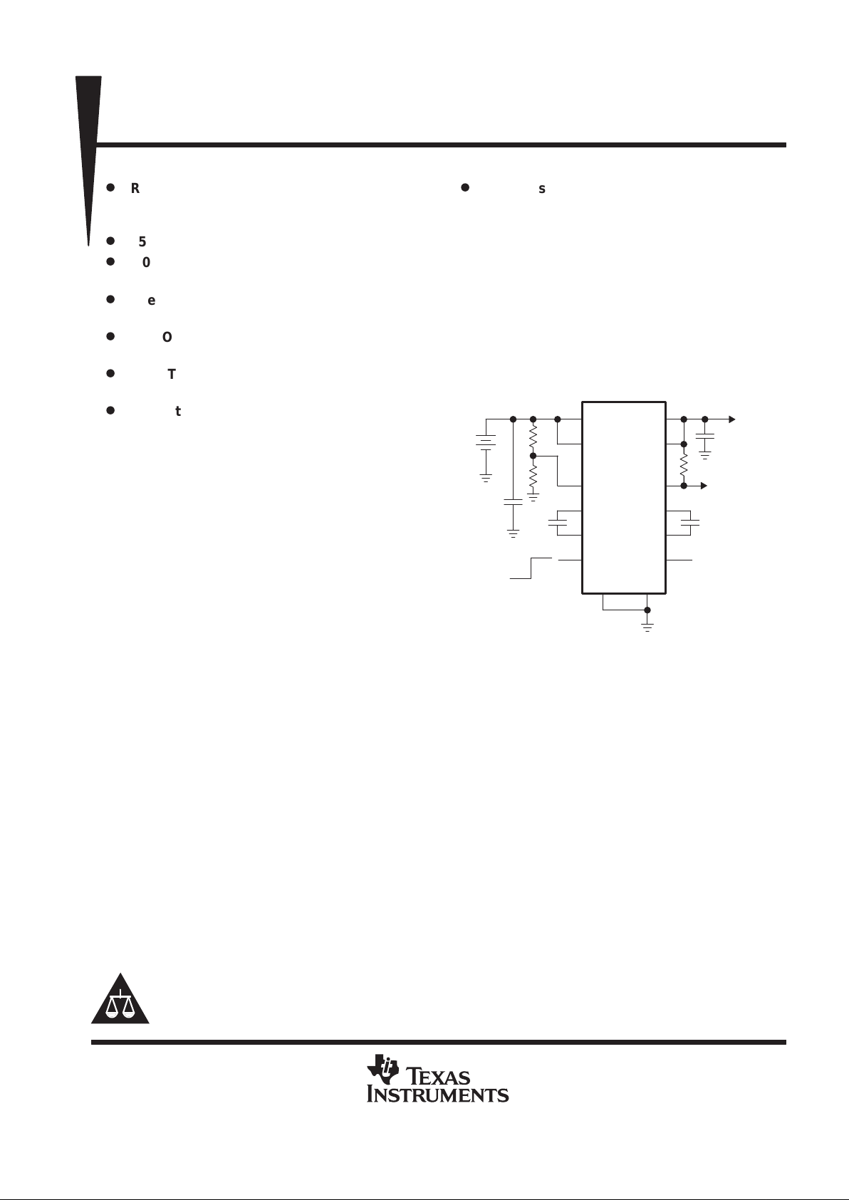
typical operating circuit
IN OUT
TPS60140
IN FB
LBI LBO
Low
Battery
Warning
Output
5 V, 100 mA
C
o
10 µF
R3
R1
R2
C2+
C2–
C2
2.2 µF
C1+
C1–
C1
2.2 µF
NC
ENABLE
PGND
GND
OFF/ON
C
i
4.7 µF
Input
1.8 V to 3.6 V
Copyright 2000, Texas Instruments Incorporated
Please be aware that an important notice concerning availability, standard warranty, and use in critical applications of
Texas Instruments semiconductor products and disclaimers thereto appears at the end of this data sheet.
PowerPAD is a trademark of Texas Instruments Incorporated.
PRODUCTION DATA information is current as of publication date.
Products conform to specifications per the terms of Texas Instruments
standard warranty. Production processing does not necessarily include
testing of all parameters.
TPS60140, TPS60141
LOW POWER DC-DC CONVERTER
REGULATED 5 V, 100-mA CHARGE PUMP VOLTAGE TRIPLER
SLVS273– FEBRUAR Y 2000
2
POST OFFICE BOX 655303 • DALLAS, TEXAS 75265
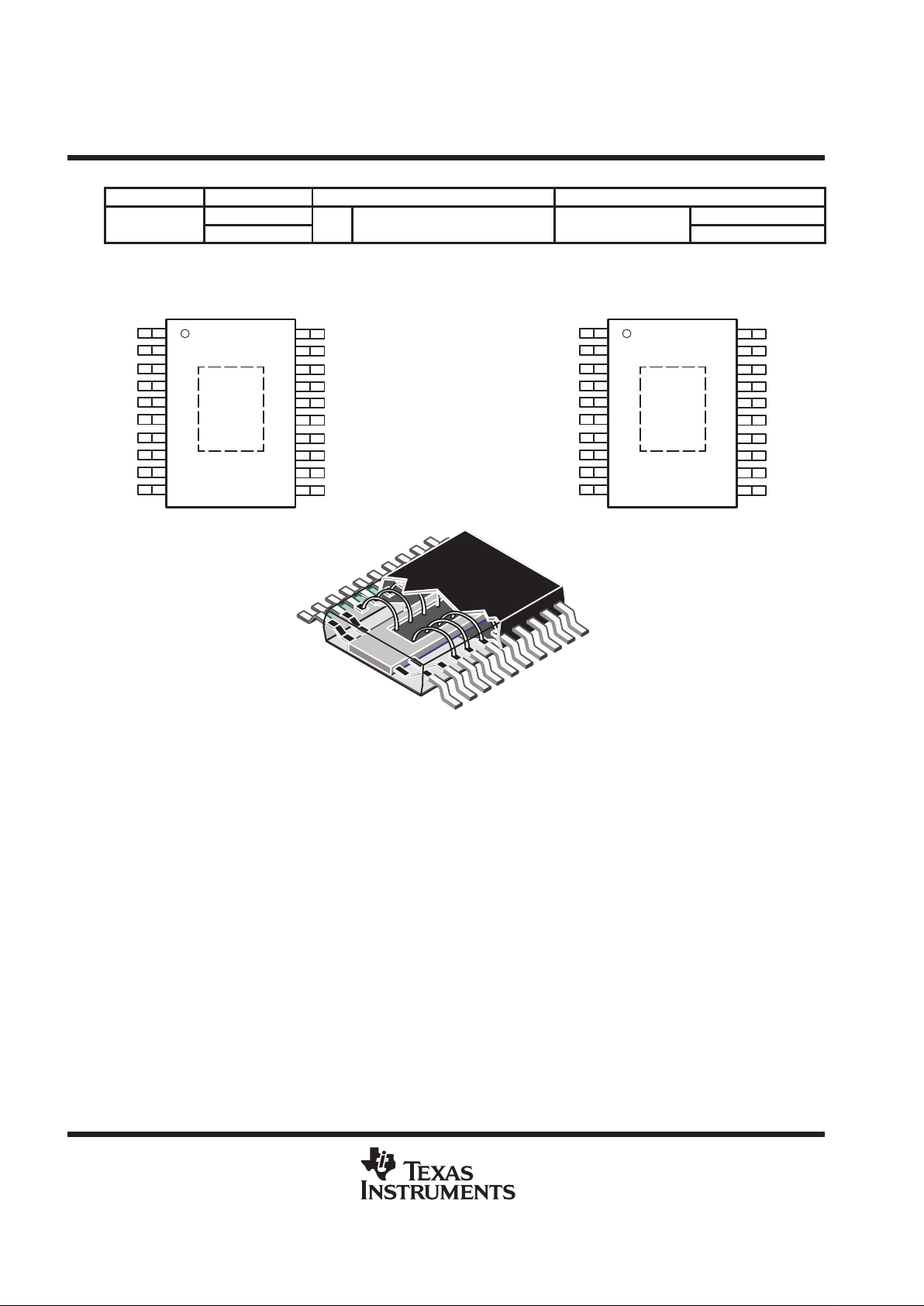
AVAILABLE OPTIONS
T
A
PART NUMBER
†
PACKAGE DEVICE FEATURES
°
°
TPS60140PWP
p
Low-battery detector
–
40°C to 85°C
TPS60141PWP
PWP
20-in thermally enhanced TSSOP
2-cell to 5 V, 100 mA
Power-good detector
†
The PWP package is available taped and reeled. Add an R suffix to the device type (e.g. TPS60140PWPR) to order quantities of 2000
devices per reel.
1
2
3
4
5
6
7
8
9
10
20
19
18
17
16
15
14
13
12
11
GND
GND
ENABLE
FB
OUT
C1+
IN
C1–
PGND
PGND
GND
GND
LBI
LBO
NC
C2+
IN
C2–
PGND
PGND
PWP PACKAGE (TPS60140)
(TOP VIEW)
1
2
3
4
5
6
7
8
9
10
20
19
18
17
16
15
14
13
12
11
GND
GND
ENABLE
FB
OUT
C1+
IN
C1–
PGND
PGND
GND
GND
NC
PG
NC
C2+
IN
C2–
PGND
PGND
PWP PACKAGE (TPS60141)
(TOP VIEW)
TPS60140, TPS60141
LOW POWER DC-DC CONVERTER
REGULATED 5 V, 100-mA CHARGE PUMP VOLTAGE TRIPLER
SLVS273– FEBRUAR Y 2000
3
POST OFFICE BOX 655303 • DALLAS, TEXAS 75265
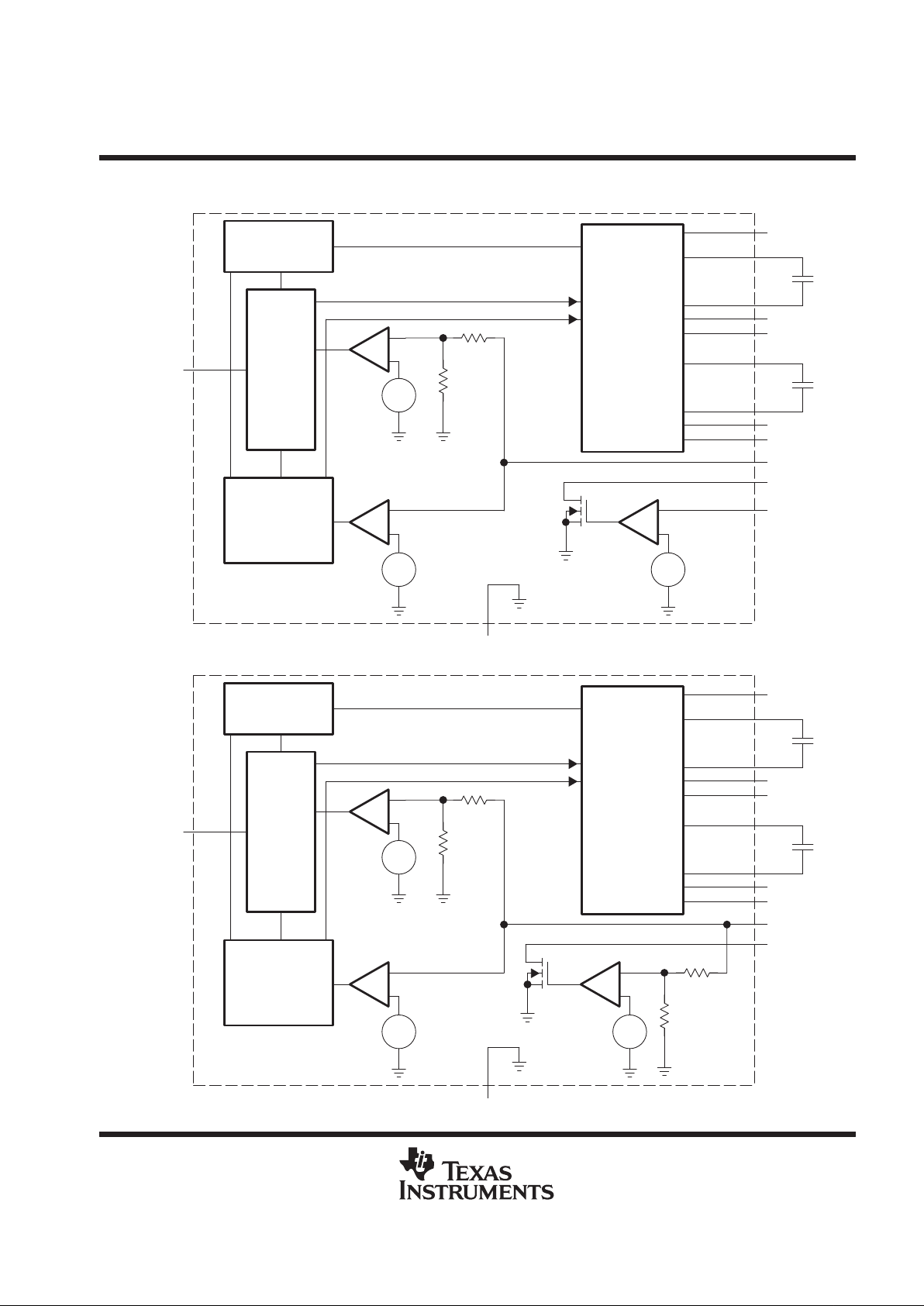
functional block diagrams
Charge Pump
Power Stage
C1
C1–
C1+
IN
PGND
C2
C2–
C2+
IN
OUT
PGND
Oscillator
Control
Circuit
ENABLE
Shutdown/
Start-up Control
_
+
+
–
V
REF
_
+
+
–
0.8 × V
I
GND
FB
_
+
+
–
V
REF
LBI
LBO
TPS60140
Charge Pump
Power Stage
C1
C1–
C1+
IN
PGND
C2
C2–
C2+
IN
OUT
PGND
Oscillator
Control
Circuit
ENABLE
Shutdown/
Start-up Control
_
+
+
–
V
REF
_
+
+
–
0.8 × V
I
FB
_
+
+
–
V
REF
PG
TPS60141
GND
TPS60140, TPS60141
LOW POWER DC-DC CONVERTER
REGULATED 5 V, 100-mA CHARGE PUMP VOLTAGE TRIPLER
SLVS273– FEBRUAR Y 2000
4
POST OFFICE BOX 655303 • DALLAS, TEXAS 75265
Terminal Functions
TERMINAL
NAME NO.
I/O
DESCRIPTION
C1+ 6 Positive terminal of the flying capacitor C1
C1– 8 Negative terminal of the flying capacitor C1
C2+ 15 Positive terminal of the flying capacitor C2
C2– 13 Negative terminal of the flying capacitor C2
ENABLE 3 I
ENABLE input. Connect ENABLE to IN for normal operation. When ENABLE is a logic low, the device turns off and
the supply current decreases to 0.05 µA. The output is disconnected from the input when the device is placed in
shutdown.
FB 4 I
Feedback input. Connect FB to OUT as close to the load as possible to achieve best regulation. A resistive divider
is on the chip to match the output voltage to the internal reference voltage of 1.21 V .
GND
1, 2,
19, 20
Ground. Analog ground for internal reference and control circuitry. Connect to PGND through a short trace.
IN 7,14 I Supply input. Bypass IN to PGND with capacitor Ci. Connect both IN terminals through a short trace.
LBO/PG 17 O
Low battery detector output (TPS60140) or power good output (TPS60141). Open drain output of the low-battery
indicator or power-good comparator . It can sink 1 mA. A 100-kΩ to 1-MΩ pullup is recommended. Leave the terminal
unconnected if the low-battery or power-good detector function is not used.
LBI/NC 18 I
Low battery detector input (TPS60140 only). The voltage applied to this terminal is compared to the internal 1.21-V
reference voltage. Connect the terminal to ground if the low-battery comparator is not used. On the TPS60141, this
terminal is not connected to the chip and should remain unconnected.
NC 16 Not connected
OUT 5 O Regulated 5-V power output. Bypass OUT to PGND with the output filter capacitor C
o.
PGND 9–12 Power ground. The charge-pump current flows through this terminal. Connect all PGND terminals together.
detailed description
The TPS6014x charge pumps provide a regulated 5-V output from a 1.8-V to 3.6-V input voltage range. They
can deliver a maximum continuous load current of at least 100 mA at VI = 2 V minimum. Designed specifically
for space-critical battery-powered applications, the complete charge pump circuit requires only four external
capacitors.
The TPS6014x consist of an oscillator, a 1.21-V voltage reference, an internal resistive feedback circuit, an error
amplifier, high current MOSFET switches, a shutdown/start-up circuit, a low-battery or power-good comparator
and a control circuit (see the functional block diagrams).
operating principle
The TPS6014x devices regulate the output voltage using an improved pulse-skip topology . In pulse-skip mode
the error amplifier disables switching of the power stages when it detects an output voltage higher than 5 V.
The oscillator halts and the controller skips switching cycles. The error amplifier reactivates the oscillator and
starts switching of the power stages again when the output voltage drops below 5 V. The output resistance of
the charge pump is controlled to improve the ripple performance. This limits the output current to the minimum
that is necessary to sustain a regulated output voltage. The benefit is that the ripple performance is nearly as
good as with a linear-regulation topology.
At light loads a conventional pulse-skip regulation mode is used, but the charge pump output resistance is held
at a high level. The pulse-skip regulation minimizes the operating current because the charge pump does not
switch continuously and hence the gate-charge losses of the MOSFET s are reduced. Additionally, all functions
except voltage reference, error amplifier, and low-battery or power-good comparator are deactivated when the
output is higher than 5 V. When switching is disabled by the error amplifier, the load is also isolated from the
input. This improved pulse-skip control topology is also referred to as
active-cycle
control.
TPS60140, TPS60141
LOW POWER DC-DC CONVERTER
REGULATED 5 V, 100-mA CHARGE PUMP VOLTAGE TRIPLER
SLVS273– FEBRUAR Y 2000
5
POST OFFICE BOX 655303 • DALLAS, TEXAS 75265
detailed description (continued)
start-up procedure and shutdown
During start-up, i.e., when ENABLE is set from logic low to logic high, the output capacitor is charged up with
a limited current until the output voltage(VO) reaches 0.8 x VI. When the start-up comparator detects this voltage
limit, the IC begins switching. This pre-charging of the output capacitor ensures a short start-up time. In addition,
the inrush current into an empty output capacitor is limited because the current through the switches is limited
before the charge pump starts switching.
Driving ENABLE low places the device in shutdown mode. This disables all switches, the oscillator, and control
logic. The device typically draws 0.05 µA of supply current in this mode. Leakage current drawn from the output
is as low as 1 µA max. The device exits shutdown once ENABLE is set to a high level. When the device is in
shutdown, the load is isolated from the input.
undervoltage lockout and short-circuit protection
The TPS6014x devices have an undervoltage lockout feature that deactivates the device and places it in
shutdown mode when the input voltage falls below 1.6 V . The devices are also short-circuit protected. The output
current is limited to typically 100 mA during a hard short circuit condition at the output, i.e., when V
O
is GND.
In this case the condition to enter the start-up mode is met, the device stops switching and controls the
on-resistance of the appropriate MOSFET switches to limit the current.
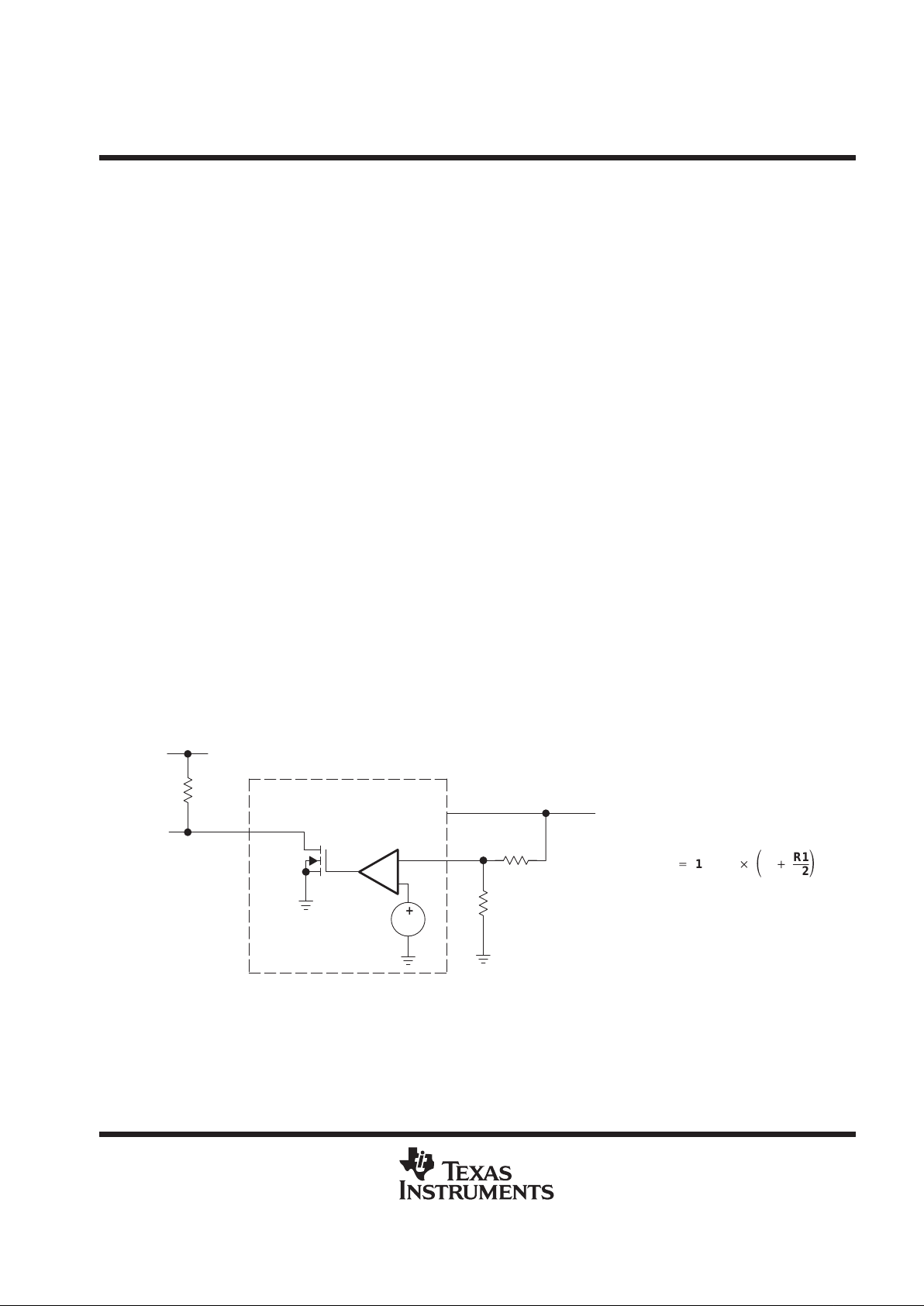
low-battery detector (TPS60140 only)
The internal low-battery comparator trips at 1.21 V ±5% when the voltage on pin LBI ramps down. The voltage
V
(TRIP)
at which the low battery warning is issued can be adjusted with a resistive divider as shown in Figure 1.
The sum of resistors R1 and R2 is recommended to be in the 100 kΩ to 1 MΩ range. When choosing R1 and
R2, be aware of the input leakage current into the LBI terminal.
LBO is an open drain output. An external pullup resistor to OUT , in the 100 kΩ to 1 MΩ range, is recommended.
During start-up, the LBO output signal is invalid for the first 500 µs. LBO is high impedance when the device
is disabled. If the low-battery comparator function is not used, connect LBI to ground and leave LBO
unconnected.
V
(TRIP)
+
1.21 V
ǒ1
)
R1
R2
Ǔ
V
O
_
+
+
–
V
REF
V
BAT
R2
R1
LBI
IN
LBO
R3
Figure 1. Programming of the Low-Battery Comparator Trip Voltage
A 100 nF ceramic capacitor should be connected in parallel to R2 if large line transients are expected. These
voltage drops can inadvertently trigger the low-battery comparator and produce a wrong low-battery warning
signal at the LBO pin.
TPS60140, TPS60141
LOW POWER DC-DC CONVERTER
REGULATED 5 V, 100-mA CHARGE PUMP VOLTAGE TRIPLER
SLVS273– FEBRUAR Y 2000
6
POST OFFICE BOX 655303 • DALLAS, TEXAS 75265
low-battery detector (TPS60140 only) (continued)
Formulas to calculate the resistive divider for low battery detection, with V
(LBI)
= 1.15 V to 1.27 V:
R2+1MΩ x
V
LBI
V
Bat
R1+1MΩ –R2
Formulas to calculate the minimum and maximum trip voltage:
V
trip(min)
+
V
LBI(min)
R1
(min)
)
R2
(max)
R2
(max)
V
trip(max)
+
V
LBI(max)
R1
(max)
)
R2
(min)
R2
(min)
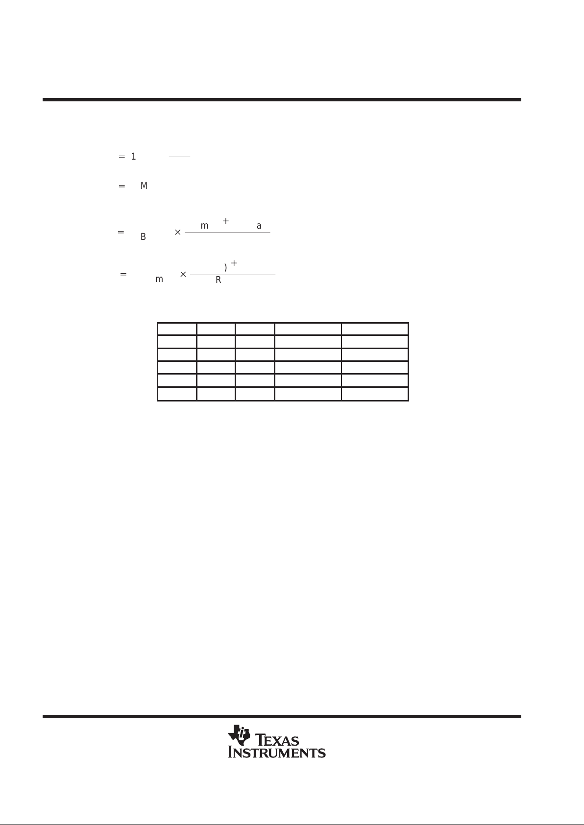
Table 1. Recommended Values for the Resistive Divider From the E96 Series (±1%)
VI/V R1/kΩ R2/kΩ V
(TRIP)
MIN/V V
(TRIP)
MAX/V
1.8 357 732 1.700 1.902
1.9 365 634 1.799 2.016
2.0 412 634 1.883 2.112
2.1 432 590 1.975 2.219
2.2 442 536 2.080 2.338
power-good detector (TPS60141)
The PG terminal is an open-drain output that is pulled low when the output is out of regulation. When the output
rises to typically 90% of its nominal voltage, the power-good output is released. Power-good is high impedance
in shutdown. In normal operation an external pullup resistor must be connected between PG and OUT. The
resistor should be in the 100 kΩ to 1 MΩ range. If the power-good function is not used, the PG terminal should
remain unconnected.
absolute maximum ratings over operating free-air temperature range (unless otherwise noted)
†‡
Supply voltage range at IN to GND and PGND –0.3 V to 3.6 V. . . . . . . . . . . . . . . . . . . . . . . . . . . . . . . . . . . . . . . .
Voltage range, at OUT, ENABLE, LBI, LBO, PG, FB to GND and PGND –0.3 V to 5.4 V. . . . . . . . . . . . . . . . . .
Voltage range at C1+ TO GND –0.3 V to (VO + 0.3 V). . . . . . . . . . . . . . . . . . . . . . . . . . . . . . . . . . . . . . . . . . . . . . .
Voltage range at C1– TO GND –0.3 V to (VI + 0.3 V). . . . . . . . . . . . . . . . . . . . . . . . . . . . . . . . . . . . . . . . . . . . . . . .
Voltage range at C2+ TO GND –0.3 V to (VO + 0.3 V). . . . . . . . . . . . . . . . . . . . . . . . . . . . . . . . . . . . . . . . . . . . . . .
Voltage range at C2– TO GND –0.3 V to (VI + 0.3 V). . . . . . . . . . . . . . . . . . . . . . . . . . . . . . . . . . . . . . . . . . . . . . . .
Continuous output current 150 mA. . . . . . . . . . . . . . . . . . . . . . . . . . . . . . . . . . . . . . . . . . . . . . . . . . . . . . . . . . . . . . . .
Storage temperature range, T
stg
–55°C to 150°C. . . . . . . . . . . . . . . . . . . . . . . . . . . . . . . . . . . . . . . . . . . . . . . . . . . .
Lead temperature 1,6 mm (1/16 inch) from case for 10 seconds 260°C. . . . . . . . . . . . . . . . . . . . . . . . . . . . . . . .
Maximum junction temperature, T
J
150°C. . . . . . . . . . . . . . . . . . . . . . . . . . . . . . . . . . . . . . . . . . . . . . . . . . . . . . . . .
†
Stresses beyond those listed under “absolute maximum ratings” may cause permanent damage to the device. These are stress ratings only, and
functional operation of the device at these or any other conditions beyond those indicated under “recommended operating conditions” is not
implied. Exposure to absolute-maximum-rated conditions for extended periods may affect device reliability.
‡
V
(ENABLE)
, V
(LBI)
, V
(LBO),
and V
(PG)
can exceed VI up to the maximum rated voltage without increasing the leakage current drawn
by these inputs.
(1)
(2)
(3)
(4)

TPS60140, TPS60141
LOW POWER DC-DC CONVERTER
REGULATED 5 V, 100-mA CHARGE PUMP VOLTAGE TRIPLER
SLVS273– FEBRUAR Y 2000
7
POST OFFICE BOX 655303 • DALLAS, TEXAS 75265
recommended operating conditions
MIN MAX UNIT
Input voltage, V
I
1.8 3.6 V
Continuous output current, IOmax 100 mA
Operating junction temperature, T
J
125 °C
electrical characteristics at C
i
= 4.7 µF, C1 = C2 = 2.2 µF, Co = 10 µF† at TC = –40°C to 85°C, VI = 2 V,
FB = V
O
and ENABLE = VI (unless otherwise noted)
PARAMETER TEST CONDITIONS MIN TYP MAX UNIT
V
(UVLO)
Undervoltage lockout threshold TC = 25°C 1.6 1.8 V
IOmax Maximum continuous output current 100 mA
V
O
Output voltage
1.8 V < VI < 2 V,
VO Start-up = 5 V ,
0 < IO < IOmax/2
TC = 0°C to 70°C
4.8 5.2
V
2 V < VI < 3.6 V,
0 < IO < IOmax
4.8 5.2
I
lkg(OUT)
Output leakage current VI = 2.4 V , V
(ENABLE)
= GND 1 µA
I
Q
Quiescent current (no-load input current) VI = 2.4 V 65 90 µA
I
(SD)
Shutdown current VI = 2.4 V , V
(ENABLE)
= GND 0.05 1 µA
f
(OSC)
Oscillator frequency 210 320 450 kHz
V
IL
ENABLE input voltage low VI = 1.8 V 0.3 × V
I
V
V
IH
ENABLE input voltage high VI = 3.6 V 0.7 × V
I
V
I
lkg(ENABLE)
ENABLE input leakage current V
(ENABLE)
= GND or V
I
0.01 0.1 µA
Output load regulation
VI = 2.4 V,
1 mA < IO < IOmax,
TC = 25°C
0.003 %/mA
Output line regulation
2 V < VI < 3.6 V,
VO = 5 V: IO = 75 mA,
TC = 25°C
0.08 %/V
I
(SC)
Short circuit current limit
VI < 2.4 V, VO = 0 V,
TC = 25°C
100 mA
V
(TRIP,LBI)
LBI trip voltage TPS60140
VI = 1.8 V to 2.2 V,
Hysteresis 0.8% for rising LBI
voltage,
TC = 0°C to 70°C
1.15 1.21 1.27 V
I
I(LBI)
LBI input current TPS60140 LBI = 1.3 V 20 100 nA
V
O(LBO)
LBO output voltage low
‡
TPS60140
V
(LBI)
= 0 V,
I
(LBO,SINK)
= 1 mA
0.4 V
I
lkg(LBO)
LBO output leakage current TPS60140 V
(LBI)
= 1.3 V, V
(LBO)
= 5 V 0.01 0.1 µA
V
(TRIP,PG)
Power-good trip voltage TPS60141 TC = 0°C to 70°C
0.86 ×
V
O
0.90 ×
V
O
0.94 ×
V
O
V
V
hys(PG)
Power-good trip voltage hysteresis TPS60141
VO ramping down,
TC = 0°C to 70°C
0.8%
V
O(PG)
Power-good output voltage low TPS60141 VO = 0 V, I
(PG,SINK)
= 1 mA 0.4 V
I
lkg(PG)
Power-good leakage current TPS60141 VO = 5 V, V
(PG)
= 5 V 0.01 0.1 µA
†
All capacitors are ceramic capacitors of the type X5R or X7R.
‡
During start-up the LBO signal is invalid for the first 500 µs.
TPS60140, TPS60141
LOW POWER DC-DC CONVERTER
REGULATED 5 V, 100-mA CHARGE PUMP VOLTAGE TRIPLER
SLVS273– FEBRUAR Y 2000
8
POST OFFICE BOX 655303 • DALLAS, TEXAS 75265
PARAMETER MEASUREMENT INFORMATION
IN OUT
TPS6014x
IN FB
LBI LBO
C
o
10 µF
R1
R2
C2+
C2–
C2
2.2 µF
C1+
C1–
C1
2.2 µF
ENABLE
PGND
GND
OFF/ON
C
i
4.7 µF
Used Capacitor Types:
Ci, Co: Ceramic, X7R, Size 1206
C1, C2: Ceramic, X7R, Size 1206
OUT
Figure 2. Circuit Used For Typical Characteristics Measurements
TYPICAL CHARACTERISTICS
Table of Graphs
FIGURE
vs Output Current 3
η
Efficienc
y
vs Input Voltage
4
I
Q
Quiescent Supply Current vs Input Voltage 5
p
vs Output Current 6
VOOutput Voltage
vs Input Voltage 7
V
O
Output Voltage Ripple 8,9,10
p
pp
p
vs Input Voltage 11
VPPOutput Voltage Ripple Amplitude
vs Output Current 12
f
(OSC)
Oscillator Frequency vs Input Voltage 13
Load Transient Response 14
Line Transient Response 15
V
O
Output Voltage vs T ime (Start-up Timing) 16

TPS60140, TPS60141
LOW POWER DC-DC CONVERTER
REGULATED 5 V, 100-mA CHARGE PUMP VOLTAGE TRIPLER
SLVS273– FEBRUAR Y 2000
9
POST OFFICE BOX 655303 • DALLAS, TEXAS 75265
TYPICAL CHARACTERISTICS
30
40
50
60
70
80
90
IO – Output Current – mA
VI = 2.0 V
EFFICIENCY
vs
OUTPUT CURRENT
0.1 10 100 10001
VI = 2.4 V
VI = 2.7 V
Figure 3
Efficiency – %
VI – Input Voltage – V
40
50
60
70
80
90
1.8 2.0 2.2 2.4 2.6 2.8 3.0 3.2 3.4 3.6
IO = 50 mA
EFFICIENCY
vs
INPUT VOLTAGE
Figure 4
Efficiency – %
VI – Input Voltage – V
50
55
60
65
70
75
1.8 2.0 2.2 2.4 2.6 2.8 3.0 3.2 3.4 3.6
TA = 25°C
QUIESCENT SUPPLY CURRENT
vs
INPUT VOLTAGE
TA = –40°C
TA = 85°C
Figure 5
– Supply Current –
A
µ
I
CC
4.8
4.85
4.90
4.95
5.00
5.05
5.10
IO – Output Current – mA
VI = 2.4 V
OUTPUT VOLTAGE
vs
OUTPUT CURRENT
0.1 10 100 10001
VI = 3.6 V
VI = 2.7 V
VI = 1.8 V
Figure 6
V
O
– Output Voltage – V
TPS60140, TPS60141
LOW POWER DC-DC CONVERTER
REGULATED 5 V, 100-mA CHARGE PUMP VOLTAGE TRIPLER
SLVS273– FEBRUAR Y 2000
10
POST OFFICE BOX 655303 • DALLAS, TEXAS 75265
TYPICAL CHARACTERISTICS
VI – Input Voltage – V
4.80
4.85
4.90
4.95
5.00
5.05
5.10
1.8 2.0 2.2 2.4 2.6 2.8 3.0 3.2 3.4 3.6
OUTPUT VOLTAGE
vs
INPUT VOLTAGE
IO = 1 mA
IO = 50 mA
Figure 7
V
O
– Output Voltage – V
IO = 100 mA
Figure 8
V
O
– Output Voltage – V
OUTPUT VOLTAGE RIPPLE
4.85
4.90
5.15
5.25
5.20
5.10
5.05
4.95
5.00
0 50050 450400350300250100 150 200
t – Time – µs
VI = 2.4 V
IO = 1 mA
Figure 9
V
O
– Output Voltage – V
OUTPUT VOLTAGE RIPPLE
4.85
4.90
5.15
5.25
5.20
5.10
5.05
4.95
5.00
0505454035302510 15 20
t – Time – µs
VI = 2.4 V
IO = 10 mA
Figure 10
V
O
– Output Voltage – V
OUTPUT VOLTAGE RIPPLE
4.97
4.99
5.09
5.13
5.11
5.07
5.05
5.01
5.03
02021816141210468
t – Time – µs
VI = 2.4 V
IO = 100 mA
TPS60140, TPS60141
LOW POWER DC-DC CONVERTER
REGULATED 5 V, 100-mA CHARGE PUMP VOLTAGE TRIPLER
SLVS273– FEBRUAR Y 2000
11
POST OFFICE BOX 655303 • DALLAS, TEXAS 75265
TYPICAL CHARACTERISTICS
– Output Voltage Ripple Amplitude –
VI – Input Voltage – V
0
10
20
30
40
50
60
1.8 2.0 2.2 2.4 2.6 2.8 3.0 3.2 3.4 3.6
OUTPUT VOLTAGE RIPPLE AMPLITUDE
vs
INPUT VOLTAGE
IO = 1 mA
IO = 10 mA
IO = 100 mA
Figure 11
V
pp
mV
IO – Output Current – mA
0
10
20
30
40
50
60
0 102030405060708090100
OUTPUT VOLTAGE RIPPLE AMPLITUDE
vs
OUTPUT CURRENT
VI = 2.4 V
Figure 12
– Output Voltage Ripple Amplitude –
V
pp
mV
VI – Input Voltage – V
300
305
310
315
320
325
330
1.8 2.0 2.2 2.4 2.6 2.8 3.0 3.2 3.4 3.6
TA = 25°C
OSCILLATOR FREQUENCY
vs
INPUT VOLTAGE
TA = –40°C
TA = 85°C
Figure 13
– Oscillator Frequency –
f
(OSC)
kHz
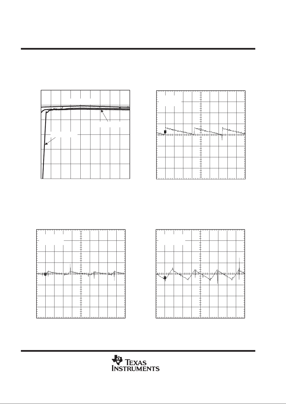
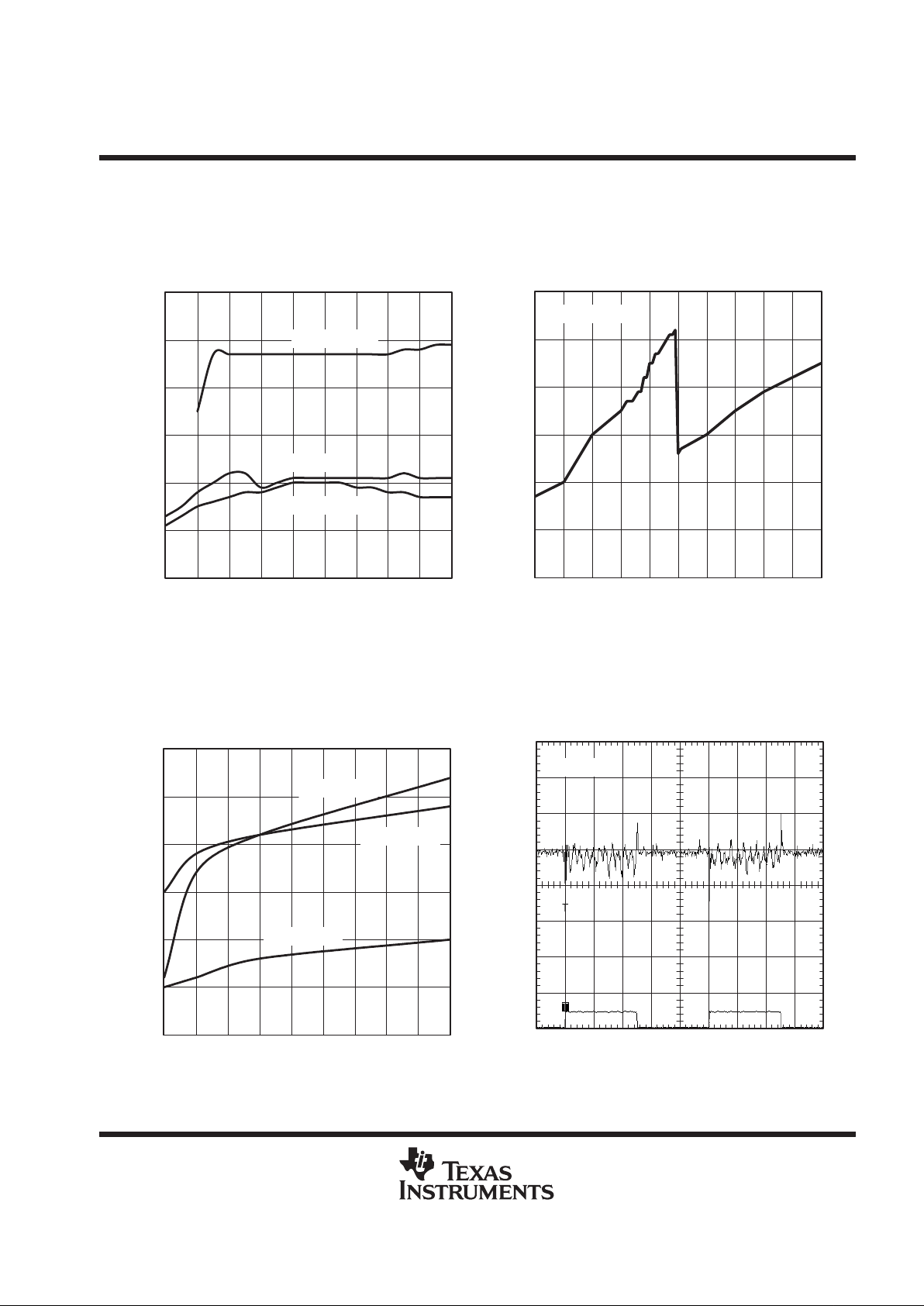
Figure 14
I
O
V
O
– Output Voltage – V
– Output Current – mA
0
260
5.07
5.05
5.03
VI = 2.4 V
LOAD TRANSIENT RESPONSE
02021816141210468
t – Time – ms

TPS60140, TPS60141
LOW POWER DC-DC CONVERTER
REGULATED 5 V, 100-mA CHARGE PUMP VOLTAGE TRIPLER
SLVS273– FEBRUAR Y 2000
12
POST OFFICE BOX 655303 • DALLAS, TEXAS 75265
TYPICAL CHARACTERISTICS
Figure 15
V
I
V
O
– Output Voltage – V
– Input Voltage – V
LINE TRANSIENT RESPONSE
2.0
2.5
5.07
5.05
5.03
3.0
02021816141210468
t – Time – ms
IO = 50 mA
t – Time – ms
–1
0
1
2
3
4
5
6
–0.1 0.0 0.1 0.2 0.3 0.4 0.5 0.6
OUTPUT VOLTAGE
vs
TIME (START-UP TIMING)
VI = 2.4 V
IO = 100 mA
–1
0
1
2
3
4
5
6
Out
Enable
Figure 16
V
O
– Output Voltage – V
Enable Voltage – V
APPLICATION INFORMATION
capacitor selection
The TPS6014x requires only four external capacitors as shown in the basic application circuit. Their capacitance
values are closely linked to the output current and output ripple requirements. For lowest ripple, low ESR
(< 0.1 Ω) capacitors should be used at the input and output of the charge pump.
The input capacitor improves system efficiency by reducing the input impedance. It also stabilizes the input
current of the power source. The input capacitor should be chosen according to the power supply used and the
distance from the power source to the converter IC. The input capacitor selection also depends on the output
ripple requirements. Ci is recommended to be about two to four times as large as the flying capacitors. The lower
the ESR of the input capacitor C
i,
the lower is the output ripple.
The output capacitor Co can be selected from 2-times to 50-times larger than the flying capacitor, depending
on the ripple tolerance. The larger Co and the lower its ESR, the lower will be the output voltage ripple.
Generally , the flying capacitors will be the smallest. Only ceramic capacitors are recommended because of their
low ESR and because they retain their capacitance at the switching frequency . Please be aware that, depending
on the material used to manufacture them, ceramic capacitors might lose their capacitance over temperature
and voltage. Ceramic capacitors of type X7R or X5R material will keep their capacitance over temperature and
voltage, whereas Z5U or Y5V-type capacitors will decrease in capacitance. Table 2 lists recommended
capacitor values.

TPS60140, TPS60141
LOW POWER DC-DC CONVERTER
REGULATED 5 V, 100-mA CHARGE PUMP VOLTAGE TRIPLER
SLVS273– FEBRUAR Y 2000
13
POST OFFICE BOX 655303 • DALLAS, TEXAS 75265
APPLICATION INFORMATION
capacitor selection (continued)
Table 2. Recommended Capacitor Values
I
O
(mA)
C
i
(µF)
C
(xF)
(µF)
C
o
(µF)
VPPTYP
(mV)
0 – 50 4.7 2.2 4.7 40
0 – 100 4.7 2.2 10 40
0 – 100 4.7 2.2 22 18
If the measured output voltage ripple is too high for the application, improvements can be made. The first step
is to increase the capacitance at the output. If the ripple is still too high, the second step would be to increase
the capacitance at the input. For lower output currents, lower value flying capacitors can be used. T ables 3 and
4 lists the manufacturers of recommended capacitors.
Table 3. Recommended Capacitors
MANUFACTURER PART NUMBER CAPACITANCE CASE SIZE TYPE
Taiyo Yuden
LMK212BJ105KG–T 1 µF 0805 Ceramic
LMK212BJ225MG–T 2.2 µF 0805 Ceramic
LMK316BJ475KL–T 4.7 µF 1206 Ceramic
LMK325BJ106MN–T 10 µF 1210 Ceramic
LMK432226MM–T 22 µF 1812 Ceramic
AVX
0805ZC105KAT2A 1 µF 0805 Ceramic
1206ZC225KAT2A 2.2 µF 1206 Ceramic
NOTE: Case code compatibility with EIA 535BAAC and CECC30801 molded chips.
Table 4. Recommended Capacitor Manufacturers
MANUFACTURER CAPACITOR TYPE INTERNET SITE
Taiyo Yuden X7R/X5R ceramic http://www.t–yuden.com/
AVX X7R/X5R ceramic http://www.avxcorp.com/

TPS60140, TPS60141
LOW POWER DC-DC CONVERTER
REGULATED 5 V, 100-mA CHARGE PUMP VOLTAGE TRIPLER
SLVS273– FEBRUAR Y 2000
14
POST OFFICE BOX 655303 • DALLAS, TEXAS 75265
APPLICATION INFORMATION
power dissipation
The power dissipated in the TPS6014x depends mainly on input voltage and output current and is described
by the following:
P
(DISS)
+
IO ǒ3xVI–V
O
Ǔ
By observation of the above equation, it can be seen that the power dissipation is worse for the highest input
voltage V
I
and the highest output current IO. For an input voltage of 3.6 V and an output current of 100 mA, the
calculated power dissipation P
(DISS)
is 580 mW. This is also the point where the charge pump operates with its
lowest efficiency, which is only 45%, and hence with the highest power losses.
P
(DISS)
must be less than that allowed by the package rating. The thermal resistance junction to ambient of the
thermally enhanced TSSOP is 178°C/W for an unsoldered package. The thermal resistance junction to case,
with the exposed thermal pad soldered to an infinitive heat sink, is 3.5°C/W.
With the recommended maximum junction temperature of 125°C and an assumed maximum ambient operating
temperature of 85°C, the maximum allowed thermal resistance junction to ambient of the system can be
calculated as follows:
R
ΘJA
max
+
TJmax – T
A
P
(DISS)
max
+
125°C–85°C
580 mW
+
69°CńW
Using a board layout as described in the application information section, R
ΘJA
is typically 56°C/W for an
unsoldered PowerPad and 41°C/W for a soldered PowerPad.
For more information, refer to the PowerPad application report (Literature Number: SLMA002).
(5)
(6)
TPS60140, TPS60141
LOW POWER DC-DC CONVERTER
REGULATED 5 V, 100-mA CHARGE PUMP VOLTAGE TRIPLER
SLVS273– FEBRUAR Y 2000
15
POST OFFICE BOX 655303 • DALLAS, TEXAS 75265
APPLICATION INFORMATION
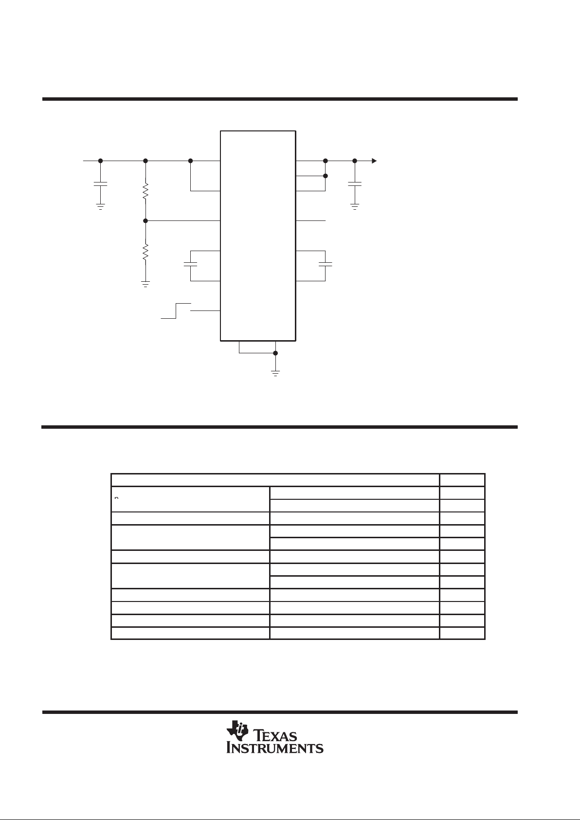
layout and board space
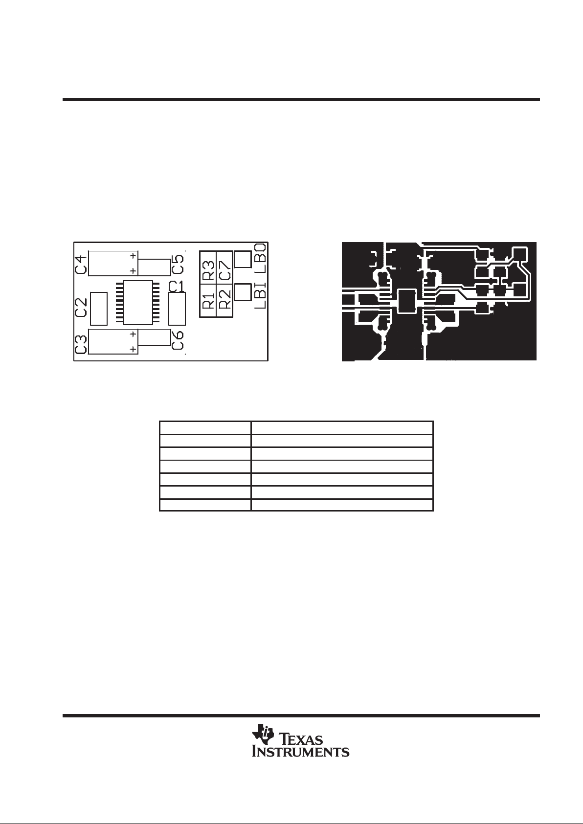
Careful board layout is necessary due to the high transient currents and switching frequency of the converter.
All capacitors should be soldered in close proximity to the IC. Connect ground and power ground terminals
through a short, low-impedance trace. A PCB layout proposal for a two-layer board is given in Figure 17. The
bottom layer of the board carries only ground potential for best performance. The layout also provides improved
thermal performance as the exposed lead frame of the PowerPad package is soldered to the PCB.
An evaluation module for the TPS60140 is available and can be ordered under product code
TPS60140EVM–144. The EVM uses the layout shown in Figure 17.
NOTE: Actual size is 15 mm x 25 mm.
Figure 17. Recommended Component Placement and Board Layout
Table 5. Component Identification
IC1 TPS6014x
C1, C2 Flying capacitors
C3, C6 Input capacitors
C4, C5 Output capacitors
C7 Stabilization capacitor for LBI
R1, R2 Resistive divider for LBI
R3 Pullup resistor for LBO
The best performance of the converter is achieved with additional bypass capacitors C5 and C6 at the input and
output. Capacitor C7 should be included if the large line transients are expected. The capacitors are not
required. They can be omitted in most applications.

TPS60140, TPS60141
LOW POWER DC-DC CONVERTER
REGULATED 5 V, 100-mA CHARGE PUMP VOLTAGE TRIPLER
SLVS273– FEBRUAR Y 2000
16
POST OFFICE BOX 655303 • DALLAS, TEXAS 75265
APPLICATION INFORMATION
related information
application reports
For more application information see:
D
PowerPAD Application Report
, Literature Number SLMA002
D
TPS6010x/TPS6011x Charge Pump Application Report
, Literature Number SLVA070
device family products
Other devices in this family are:
PART
NUMBER
DESCRIPTION
TPS60100 Regulated 3.3-V, 200-mA low-noise charge pump dc-dc converter
TPS60101 Regulated 3.3-V, 100-mA low-noise charge pump dc-dc converter
TPS60110 Regulated 5-V, 300-mA low-noise charge pump dc-dc converter
TPS60111 Regulated 5-V, 150-mA low-noise charge pump dc-dc converter
TPS60120 Regulated 3.3-V, 200-mA high efficiency charge pump dc-dc converter with low-battery comparator
TPS60121 Regulated 3.3-V, 200-mA high efficiency charge pump dc-dc converter with power-good comparator
TPS60122 Regulated 3.3-V, 100-mA high efficiency charge pump dc-dc converter with low-battery comparator
TPS60123 Regulated 3.3-V, 100-mA high efficiency charge pump dc-dc converter with power-good comparator
TPS60130 Regulated 5-V, 300-mA high efficiency charge pump dc-dc converter with low-battery comparator
TPS60131 Regulated 5-V, 300-mA high efficiency charge pump dc-dc converter with power-good comparator
TPS60132 Regulated 5-V, 150-mA high efficiency charge pump dc-dc converter with low-battery comparator
TPS60133 Regulated 5-V, 150-mA high efficiency charge pump dc-dc converter with power-good comparator

TPS60140, TPS60141
LOW POWER DC-DC CONVERTER
REGULATED 5 V, 100-mA CHARGE PUMP VOLTAGE TRIPLER
SLVS273– FEBRUAR Y 2000
17
POST OFFICE BOX 655303 • DALLAS, TEXAS 75265
MECHANICAL DATA
PWP (R-PDSO-G**) PowerPAD PLASTIC SMALL-OUTLINE
4073225/F 10/98
0,50
0,75
0,25
0,15 NOM
Thermal Pad
(See Note D)
Gage Plane
2824
7,70
7,90
20
6,40
6,60
9,60
9,80
6,60
6,20
11
0,19
4,50
4,30
10
0,15
20
A
1
0,30
1,20 MAX
1614
5,10
4,90
PINS **
4,90
5,10
DIM
A MIN
A MAX
0,05
Seating Plane
0,65
0,10
M
0,10
0°–8°
20 PINS SHOWN
NOTES: A. All linear dimensions are in millimeters.
B. This drawing is subject to change without notice.
C. Body dimensions do not include mold flash or protrusions.
D. The package thermal performance may be enhanced by bonding the thermal pad to an external thermal plane.
This pad is electrically and thermally connected to the backside of the die and possibly selected leads.
E. Falls within JEDEC MO-153
PowerPAD is a trademark of Texas Instruments Incorporated.

IMPORTANT NOTICE
T exas Instruments and its subsidiaries (TI) reserve the right to make changes to their products or to discontinue
any product or service without notice, and advise customers to obtain the latest version of relevant information
to verify, before placing orders, that information being relied on is current and complete. All products are sold
subject to the terms and conditions of sale supplied at the time of order acknowledgement, including those
pertaining to warranty, patent infringement, and limitation of liability.
TI warrants performance of its semiconductor products to the specifications applicable at the time of sale in
accordance with TI’s standard warranty. Testing and other quality control techniques are utilized to the extent
TI deems necessary to support this warranty. Specific testing of all parameters of each device is not necessarily
performed, except those mandated by government requirements.
CERT AIN APPLICATIONS USING SEMICONDUCTOR PRODUCTS MAY INVOLVE POTENTIAL RISKS OF
DEATH, PERSONAL INJURY, OR SEVERE PROPERTY OR ENVIRONMENTAL DAMAGE (“CRITICAL
APPLICATIONS”). TI SEMICONDUCTOR PRODUCTS ARE NOT DESIGNED, AUTHORIZED, OR
WARRANTED TO BE SUITABLE FOR USE IN LIFE-SUPPORT DEVICES OR SYSTEMS OR OTHER
CRITICAL APPLICATIONS. INCLUSION OF TI PRODUCTS IN SUCH APPLICA TIONS IS UNDERSTOOD T O
BE FULLY AT THE CUSTOMER’S RISK.
In order to minimize risks associated with the customer’s applications, adequate design and operating
safeguards must be provided by the customer to minimize inherent or procedural hazards.
TI assumes no liability for applications assistance or customer product design. TI does not warrant or represent
that any license, either express or implied, is granted under any patent right, copyright, mask work right, or other
intellectual property right of TI covering or relating to any combination, machine, or process in which such
semiconductor products or services might be or are used. TI’s publication of information regarding any third
party’s products or services does not constitute TI’s approval, warranty or endorsement thereof.
Copyright 2000, Texas Instruments Incorporated
 Loading...