

Texas Instruments TPS60131PWPR, TPS60132PWP, TPS60131PWP, TPS60130PWPR, TPS60130PWP Datasheet
...
TPS60130, TPS60131, TPS60132, TPS60133
REGULATED 5-V, 300 mA HIGH EFFICIENCY CHARGE PUMP
DC/DC CONVERTERS
SLVS258A – NOVEMBER 1999 – REVISED DECEMBER 1999
1
POST OFFICE BOX 655303 • DALLAS, TEXAS 75265
features applications
D
Up to 90% Efficiency From 2.7-V to 5.4-V
Input Voltage Range Because of Special
Switching Topology
D
Up to 300-mA Output Current (TPS60130
and TPS60131)
D
No Inductors Required, Low EMI
D
Regulated 5-V ±4% Output
D
Only Four External Components Required
D
60-µA Quiescent Supply Current
D
0.05-µA Shutdown Current
D
Load Disconnected in Shutdown
D
Space-Saving, Thermally-Enhanced
PowerPADt Package
D
Evaluation Module Available
(TPS60130EVM–143)
D
Battery-Powered Applications
D
Three Battery Cells to 5-V Conversion or
Point-of-Use 3.3 V to 5-V Conversion
D
Lilon Battery to 5-V Conversion
D
Portable Instruments
D
Battery-Powered Microprocessor Systems
D
Backup-Battery Boost Converters
D
PDA’s, Organizers, Laptops
D
Handheld Instrumentation
D
Medical Instruments (e.g., Glucose Meters)
D
PCMCIA and 5-V Smart Card Supply
description
The TPS6013x step-up, regulated charge pumps generate a 5-V ±4% output voltage from a 2.7-V to 5.4-V input
voltage (three alkaline, NiCd, or NiMH batteries or one Lithium or Lilon battery). The output current is 300 mA
for the TPS60130/ TPS60131 and 150 mA for the TPS60132/ TPS60133, all from a 3-V input. Only four external
capacitors are needed to build a complete high efficiency dc/dc charge pump converter. To achieve the high
efficiency over a wide input voltage range, the charge pump automatically selects between a 1.5x or doubler
conversion mode. From a 3-V input, all ICs can start with full load current.
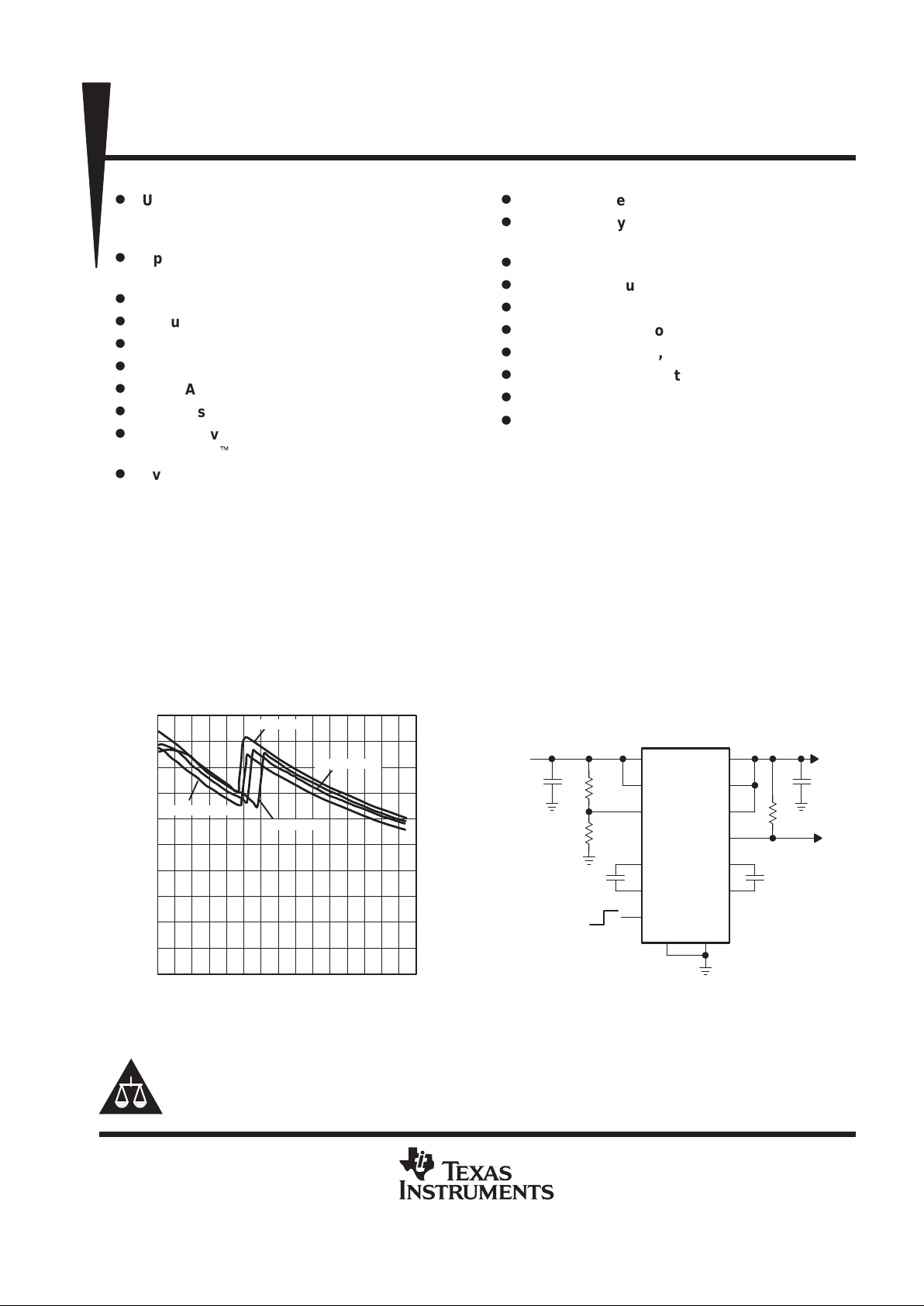
efficiency (TPS60130, TPS60131) typical operating circuit
IN
IN
LBI
C1+
C1–
ENABLE
PGND GND
OUT
OUT
FB
LBO
C2+
C2–
C
o
33 µF
C
i
15 µF
Output
5 V , 300 mA
C2
2.2 µF
C1
2.2 µF
R1
R2
Input
2.7 V to 5.4 V
OFF/ON
TPS60130
R3
IO = 66 mA
IO = 108 mA
IO = 216 mA
IO = 300 mA
60
40
20
0
2.6 3 3.4 3.8 4.2
Efficiency – %
80
90
100
4.6 5
70
50
30
10
5.4
VI – Input Voltage – V
Copyright 1999, Texas Instruments Incorporated
Please be aware that an important notice concerning availability, standard warranty, and use in critical applications of
Texas Instruments semiconductor products and disclaimers thereto appears at the end of this data sheet.
PRODUCTION DATA information is current as of publication date.
Products conform to specifications per the terms of Texas Instruments
standard warranty. Production processing does not necessarily include
testing of all parameters.
PowerPAD is a trademark of Texas Instruments Incorporated.
TPS60130, TPS60131, TPS60132, TPS60133
REGULATED 5-V, 300 mA HIGH EFFICIENCY CHARGE PUMP
DC/DC CONVERTERS
SLVS258A – NOVEMBER 1999 – REVISED DECEMBER 1999
2
POST OFFICE BOX 655303 • DALLAS, TEXAS 75265
description (continued)
The devices feature the power-saving pulse-skip mode to extend battery life at light loads. TPS60130 and
TPS60132 include a low-battery comparator; TPS60131 and TPS60133 feature a power-good output. The logic
shut-down function reduces the supply current to 1 µA (max) and disconnects the load from the input. Special
current-control circuitry prevents excessive current from being drawn from the battery during startup. This dc/dc
converter requires no inductors and therefore EMI is of low concern. It is available in the small, thermally
enhanced 20-pin PowerP ADt package (PWP).
1
2
3
4
5
6
7
8
9
10
20
19
18
17
16
15
14
13
12
11
GND
GND
ENABLE
FB
OUT
C1+
IN
C1–
PGND
PGND
GND
GND
LBI
LBO
OUT
C2+
IN
C2–
PGND
PGND
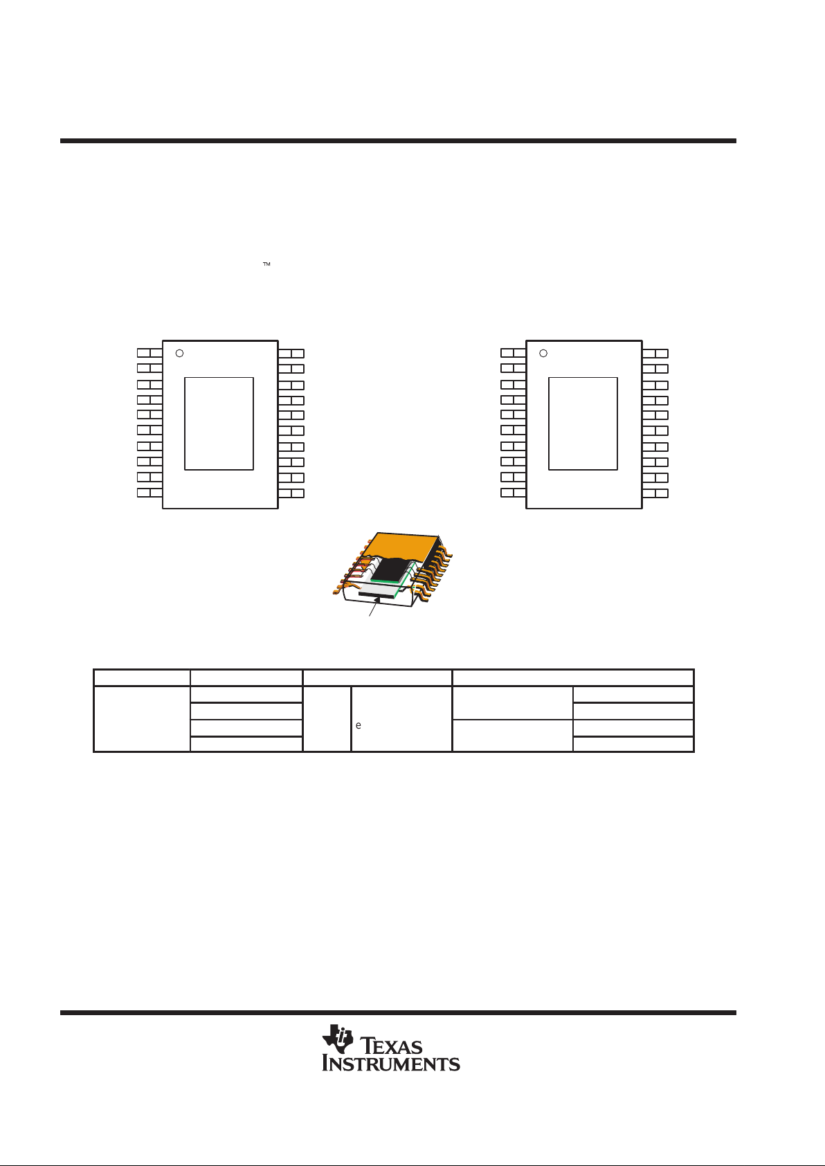
PWP PACKAGE
(TPS60130/TPS60132)
(TOP VIEW)
1
2
3
4
5
6
7
8
9
10
20
19
18
17
16
15
14
13
12
11
GND
GND
ENABLE
FB
OUT
C1+
IN
C1–
PGND
PGND
GND
GND
NC
PG
OUT
C2+
IN
C2–
PGND
PGND
PWP PACKAGE
(TPS60131/TPS60133)
(TOP VIEW)
Thermal Pad
AVAILABLE OPTIONS
T
A
PART NUMBER
†
PACKAGE DEVICE FEATURES
TPS60130PWP
Low battery detector
°
°
TPS60131PWP
20-Pin thermally
3-cell to 5 V, 300 mA
Power good detector
–
40°C to 85°C
TPS60132PWP
PWP
y
enhanced TSSOP
Low battery detector
TPS60133PWP
3-cell to 5 V, 150 mA
Power good detector
†
The PWP package is available taped and reeled. Add R suffix to device type (e.g. TPS60130PWPR) to order quanities of 2000
devices per reel.
TPS60130, TPS60131, TPS60132, TPS60133
REGULATED 5-V, 300 mA HIGH EFFICIENCY CHARGE PUMP
DC/DC CONVERTERS
SLVS258A – NOVEMBER 1999 – REVISED DECEMBER 1999
3
POST OFFICE BOX 655303 • DALLAS, TEXAS 75265
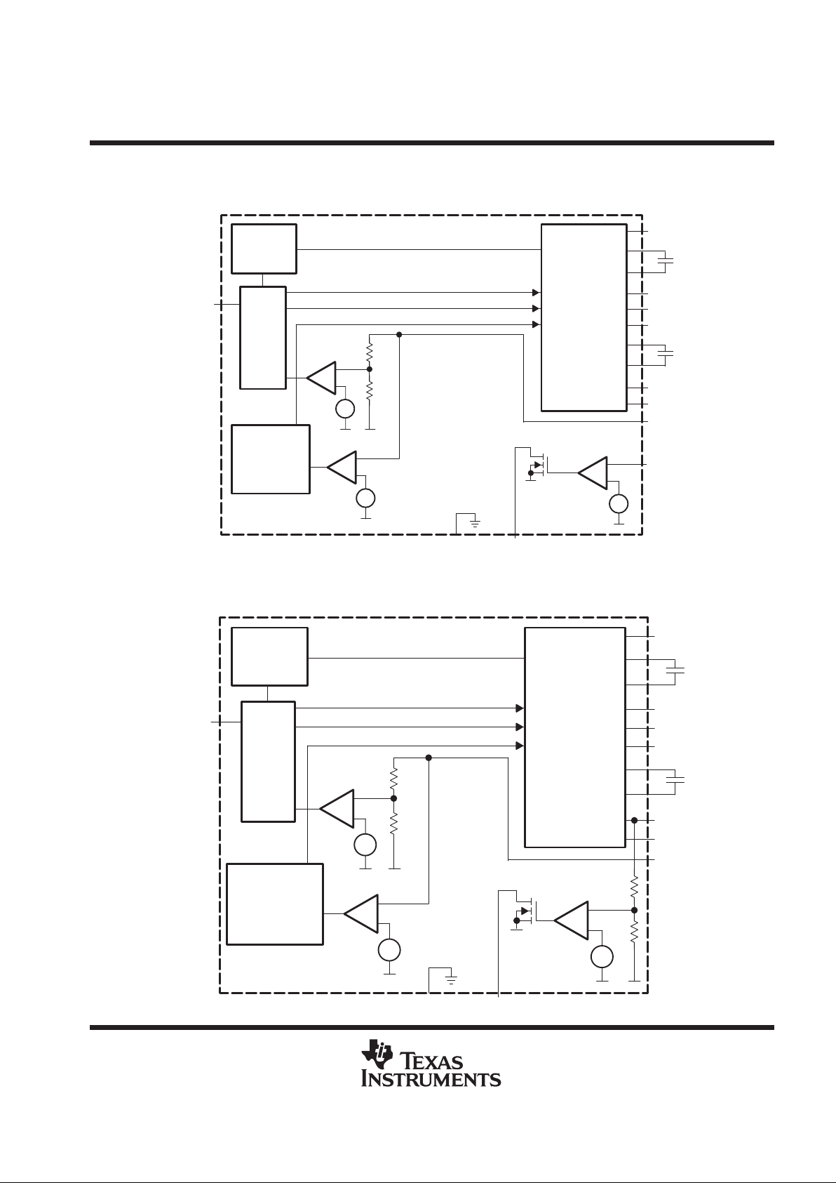
functional block diagram
_
+
Charge Pump
Power Stages
IN
C1+
C1–
OUT
PGND
IN
C2+
C2–
OUT
PGND
FB
Oscillator
Control
Circuit
_
+
+
–
V
REF
_
+
+
–
Shutdown/
Start-Up
Control
0.8 V
I
+
–
V
REF
LBI
GND LBO
ENABLE
C1F
C2F
TPS60130/TPS60132
_
+
Charge Pump
Power Stages
IN
C1+
C1–
OUT
PGND
IN
C2+
C2–
OUT
PGND
FB
Oscillator
Control
Circuit
_
+
+
–
V
REF
_
+
+
–
Shutdown/
Start-Up Control
0.8 V
I
+
–
V
REF
GND PG
ENABLE
C1F
C2F
TPS60131/TPS60133
TPS60130, TPS60131, TPS60132, TPS60133
REGULATED 5-V, 300 mA HIGH EFFICIENCY CHARGE PUMP
DC/DC CONVERTERS
SLVS258A – NOVEMBER 1999 – REVISED DECEMBER 1999
4
POST OFFICE BOX 655303 • DALLAS, TEXAS 75265
Terminal Functions
TERMINAL
NAME NO.
I/O
DESCRIPTION
C1+ 6 Positive terminal of the flying capacitor C1
C1– 8 Negative terminal of the flying capacitor C1
C2+ 15 Positive terminal of the flying capacitor C2
C2– 13 Negative terminal of the flying capacitor C2
ENABLE 3 I Enable input. Connect ENABLE to IN for normal operation. When ENABLE is a logic low, the device turns of f and
the supply current decreases to 0.05 µA. The output is disconnected from the input when the device is disabled.
FB 4 I Feedback input. Connect FB to OUT as close to the load as possible to achieve best regulation. A resistive divider
is on the chip to match internal reference voltage of 1.21 V .
GND 1, 2,
19, 20
Ground. Analog ground for internal reference and control circuitry. Connect to PGND terminals through a short
trace.
IN 7,14 I Supply input. Bypass IN to PGND with a capacitor that has half of the capacitance of the output capacitor. Connect
both IN terminals together through a short trace.
LBO/PG 17 O Low battery detector output (TPS60130 and TPS60132) or power good output (TPS60131 and TPS60133). Open
drain output of the low battery or power good comparator. It can sink 1 mA. A 100-kΩ to 1-MΩ pullup resistor to OUT
is recommended. Leave the terminal unconnected if the low battery or power good detector is not used.
LBI/NC 18 I Low battery detector input (TPS60130 and TPS60132 only). The voltage at this input is compared to the internal
1.21 V reference voltage. Connect this terminal to ground if the low-battery detection function is not used. On the
TPS60131 and TPS60133, this terminal is not connected.
OUT 5, 16 O Regulated 5-V power output. Connect both OUT terminals through a short trace and bypass OUT to GND with the
output filter capacitor C
O.
PGND 9–12 Power ground. Charge-pump current flows through this pin. Connect all PGND terminals together.
detailed description
operating principle
The TPS6013x charge pumps provide a regulated 5-V output from a 2.7-V to 5.4-V input. They deliver a
maximum load current of 300 mA or 150 mA, respectively. Designed specifically for space-critical, batterypowered applications, the complete charge pump circuit requires four external capacitors. The circuit is
optimized for efficiency over a wide input voltage range.
The TPS6013x charge pumps consist of an oscillator, a 1.21-V bandgap reference, an internal resistive
feedback circuit, an error amplifier, high current MOSFET switches, a shutdown/startup circuit, a low-battery
or power-good comparator, and a control circuit (see functional block diagrams).
The device consists of two single-ended charge pumps. These charge pumps are automatically configured to
amplify the input voltage with a conversion factor of 1.5 or 2. The conversion ratio is dependent on the input
voltage and load current. This assures high efficiency over a wide input voltage range and is further described
in the
adaptive mode switching
section below.
adaptive mode switching
The ON-resistance of the MOSFETs that are in the charge path of the flying capacitors is regulated when the
charge pump operates in voltage doubler mode. It is changed depending on the output voltage that is fed back
into the control loop. This way, the time-constant during the charging phase can be modified and increased
versus a time-constant for fully switched-on MOSFETs. The ON-resistance of both switches and the
capacitance of the flying capacitor define the time constant. The MOSFET switches in the discharge path of the
charge pump are always fully switched on to their minimum r
DS(on)
. With the time-constant during charge phase
being bigger than the time constant in discharge phase, the voltage on the flying capacitors stabilizes to the
lowest possible value necessary to get a stable V
O
.

TPS60130, TPS60131, TPS60132, TPS60133
REGULATED 5-V, 300 mA HIGH EFFICIENCY CHARGE PUMP
DC/DC CONVERTERS
SLVS258A – NOVEMBER 1999 – REVISED DECEMBER 1999
5
POST OFFICE BOX 655303 • DALLAS, TEXAS 75265
adaptive mode switching (continued)
The voltage on the flying capacitors is measured and compared with the supply voltage V
I
. If the voltage across
the flying capacitors is smaller than half of the supply voltage, then the charge pump switches into the
1.5x conversion-mode. The charge pump switches back from a 1.5x conversion-mode to a voltage doubler
mode if the load current in 1.5x conversion-mode can no more be delivered.
With this control mode the device runs in
doubler
-mode at low VI and in 1.5x conversion-mode at high VI to
optimize the efficiency. The most desirable transfer mode is automatically selected depending on both VI and
IL. This means that at light loads the device selects the 1.5x conversion-mode already at smaller supply voltages
than at heavy loads.
The TPS60130 output voltage is regulated using the
ACTIVE-CYCLE
-regulation. An active cycle controlled
charge pump utilizes two methods to control the output voltage. At high load currents it varies the on-resistances
of the internal switches and keeps the ratio ON/OFF time (=frequency) constant. That means the charge pump
runs at a fixed frequency. It also keeps the output voltage ripple as low as in linear-mode. At light loads the
internal resistance and also the amount of energy transferred per pulse is fixed and the charge pump regulates
the voltage by means of a variable ratio of ON-to-OFF time. In this operating point it runs like a skip mode
controlled charge pump with a very high internal resistance, which also enables a low ripple in this operation
mode. Since the charge pump does effectively switch at lower frequencies at light loads, it achieves a low
quiescent current.
pulse-skip mode
In pulse-skip mode the error amplifier disables switching of the power stages when it detects an output higher
than 5 V. The oscillator halts and the IC then skips switching cycles until the output voltage drops below 5 V.
The error amplifier reactivates the oscillator and starts switching the power stages again. The pulse-skip
regulation mode minimizes operating current because it does not switch continuously and deactivates all
functions except bandgap reference, error amplifier, and low-battery/power-good comparator when the output
is higher than 5 V. When switching is disabled from the error amplifier, the load is also isolated from the input.
In pulse-skip mode, a special current control circuitry, limits the peak current. This assures moderate output
voltage ripple and also prevents the device from drawing excessive current spikes out of the battery.
start-up procedure
During start-up, i.e. when ENABLE is set from logic low to logic high, the output capacitor is charged up, with
a limited current, until the output voltage V
O
reaches 0.8 × VI. When the start-up comparator detects this voltage
limit, the IC begins switching. This start-up charging of the output capacitor assures a short start-up time and
eliminates the need of a Schottky diode between IN and OUT. The IC starts with a maximum load, which is
defined by a 16-Ω or 33-Ω resistor, respectively.
shutdown
Driving ENABLE low places the device in shutdown mode. This disables all switches, the oscillator, and control
logic. The device typically draws 0.05 µA (1 µA max) of supply current in this mode. Leakage current drawn from
the output is as low as 1 µA max. The device exits shutdown once ENABLE is set to a high level. The typical
no-load shutdown exit time is 10 µs. When the device is in shutdown, the load is isolated from the input.
undervoltage lockout
The TPS6013x devices have an undervoltage lockout feature that deactivates the device and places it in
shutdown mode when the input voltage falls below 1.6 V.
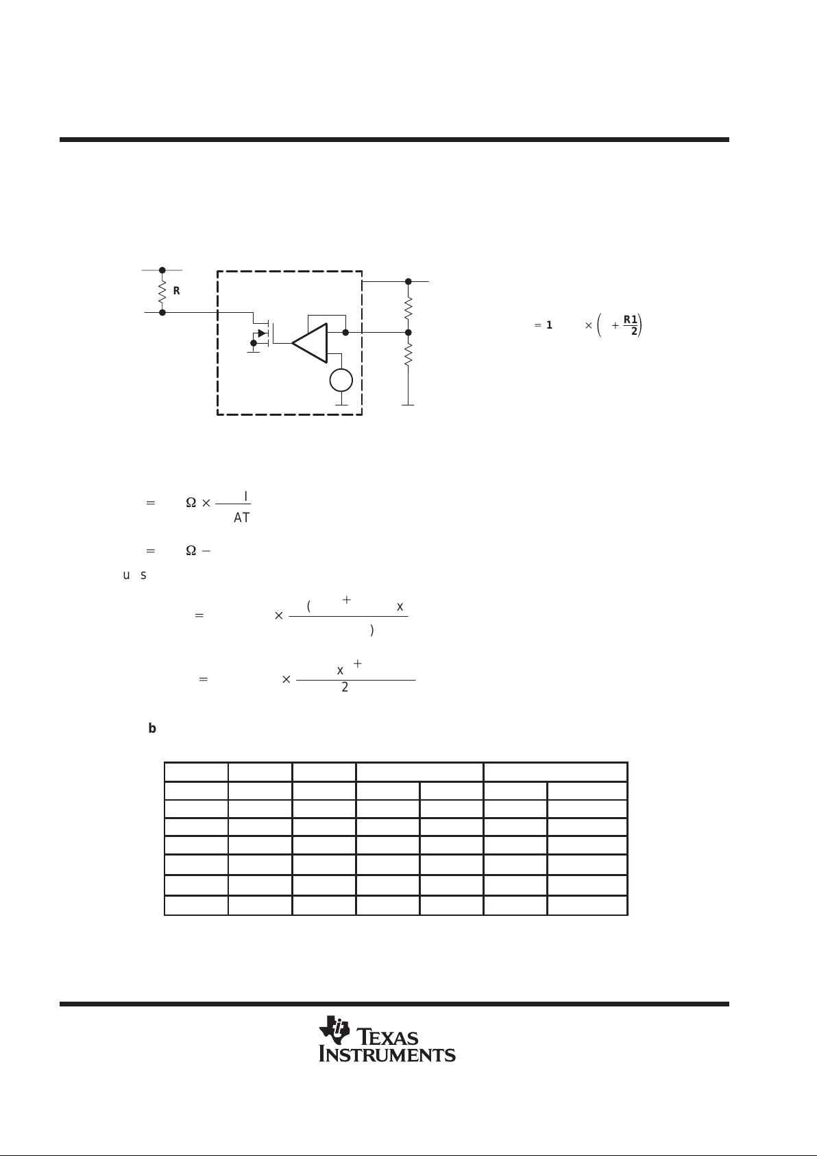
low-battery detector (TPS60130 and TPS60132)
The internal low-battery comparator trips at 1.21 V ±5% when the voltage on pin LBI ramps down. The battery
voltage at which the comparator initiates a low battery warning at the LBO output can easily be programmed
with a resistive divider as shown in Figure 3. The sum of resistors R1 and R2 is recommended to be in the 100-kΩ
to 1-MΩ range.
TPS60130, TPS60131, TPS60132, TPS60133
REGULATED 5-V, 300 mA HIGH EFFICIENCY CHARGE PUMP
DC/DC CONVERTERS
SLVS258A – NOVEMBER 1999 – REVISED DECEMBER 1999
6
POST OFFICE BOX 655303 • DALLAS, TEXAS 75265
low-battery detector (TPS60130 and TPS60132) (continued)
LBO is an open drain output. An external pullup resistor to OUT , in the 100-kΩ to 1-MΩ range is recommended.
During start-up, the LBO output signal is invalid for the first 500 µs. LBO is high impedance when the device
is disabled.
If the low-battery comparator function is not used, connect LBI to ground and leave LBO unconnected.
_
+
+
–
V
REF
V
BAT
IN
R1
LBI
R2
LBO
V
TRIP
+
1.21 V
ǒ
1
)
R1
R2
Ǔ
V
OUT
R3
Figure 1. Programming of the Low-Battery Comparator Trip Voltage
Formulas to calculate the resistive divider for low battery detection, with V
LBI
= 1.15 V – 1.27 V:
R2+1MW
V
LBI
V
BAT
R1+1MW*
R2
Formulas to calculate the minimum and maximum battery voltage that triggers the low battery detector:
V
BAT(min)
+
V
LBI(min)
R1
(min)
)
R2
(max)
R2
(max)
V
BAT(max)
+
V
LBI(max)
R1
(max)
)
R2
(min)
R2
(min)
Table 1. Recommended Values for the Resistive Divider from the E96 Series (±1%),
V
LBI
= 1.15 V – 1.27 V
V
BAT
/V R1/kΩ R2/kΩ V
BAT(MIN)
/V V
BAT(MAX)
/V
2.7 562 453 2.548 –5.61% 2.877 6.57%
2.8 576 442 2.619 –6.47% 2.958 5.66%
2.9 590 422 2.726 –6.00% 3.081 6.26%
3.0 590 402 2.804 –6.53% 3.172 5.72%
3.1 604 383 2.928 –5.56% 3.313 6.88%
3.2 619 374 3.016 –5.76% 3.414 6.70%
3.3 649 374 3.106 –5.88% 3.518 6.62%
A 100 nF bypass capacitor should be connected in parallel to R2 if large line transients are expected. These
voltage drops can inadvertently trigger the low-battery comparator and produce a wrong low-battery warning
signal at the LBO pin.
TPS60130, TPS60131, TPS60132, TPS60133
REGULATED 5-V, 300 mA HIGH EFFICIENCY CHARGE PUMP
DC/DC CONVERTERS
SLVS258A – NOVEMBER 1999 – REVISED DECEMBER 1999
7
POST OFFICE BOX 655303 • DALLAS, TEXAS 75265
Power-Good detector (TPS60131 and TPS60133)
The PG pin is an open-drain output that is pulled low when the output is out of regulation. When the output
voltage rises to about 90% of its nominal voltage, power-good output is released. PG is high impedance when
the device is disabled. An external pullup resistor must be connected between PG and OUT . The pullup resistor
should be in the 100 kΩ to 1 MΩ range. If the power-good function is not used, the PG-pin should remain
unconnected.
C
o
33 µF
Output
5 V, 300 mA
Input
2.7 V to 5.4 V
IN
IN
NC
C1+
C1–
ENABLE
PGND GND
OUT
OUT
FB
PG
C2+
C2–
C2
2.2 µF
C1
2.2 µF
Off/On
C
i
15 µF
R1
1 MΩ
TPS60131
Power-Good Output
Figure 2. Typical Operating Circuit Using Power-Good Comparator
absolute maximum ratings (see Note 1)
†
Input voltage range, VI (IN, OUT, ENABLE, FB, LBI, LBO/PG) –0.3 V to 5.5 V. . . . . . . . . . . . . . . . . . . . . . . . . . .
Differential input voltage, VID (C1+, C2+ to GND) –0.3 V to (VO + 0.3 V). . . . . . . . . . . . . . . . . . . . . . . . . . . . . .
Differential input voltage, VID (C1–, C2– to GND) –0.3 V to (VI + 0.3 V). . . . . . . . . . . . . . . . . . . . . . . . . . . . . . . .
Continuous total power dissipation See Dissipation Rating Table. . . . . . . . . . . . . . . . . . . . . . . . . . . . . . . . . . . . . .
Continuous output current: TPS60130, TPS60131 400 mA. . . . . . . . . . . . . . . . . . . . . . . . . . . . . . . . . . . . . . . . . .
TPS60132, TPS60133 200 mA. . . . . . . . . . . . . . . . . . . . . . . . . . . . . . . . . . . . . . . . . .
Storage temperature range, T
stg
–55°C to 150°C. . . . . . . . . . . . . . . . . . . . . . . . . . . . . . . . . . . . . . . . . . . . . . . . . . . .
Lead temperature 1,6 mm (1/16 inch) from case for 10s 260°C. . . . . . . . . . . . . . . . . . . . . . . . . . . . . . . . . . . . . . .
Maximum junction temperature, T
J
150°C. . . . . . . . . . . . . . . . . . . . . . . . . . . . . . . . . . . . . . . . . . . . . . . . . . . . . . . . .
†
Stresses beyond those listed under “absolute maximum ratings” may cause permanent damage to the device. These are stress ratings only, and
functional operation of the device at these or any other conditions beyond those indicated under “recommended operating conditions” is not
implied. Exposure to absolute-maximum-rated conditions for extended periods may affect device reliability.
NOTE 1: V
(ENABLE)
, V
(LBI)
and V
(LBO/PG)
can exceed VI up to the maximum rated voltage without increasing the leakage current drawn by these
inputs.
DISSIPATION RATING TABLE FREE-AIR TEMPERATURE (see Figure 1)
PACKAGE
TA ≤ 25°C
POWER RATING
DERATING FACTOR
ABOVE TA = 25°C
TA = 70°C
POWER RATING
TA = 85°C
POWER RATING
PWP 700 mW 5.6 mW/°C 448 mW 364 mW
DISSIPATION RATING T ABLE CASE TEMPERATURE (see Figure 2)
PACKAGE
TC ≤ 62.5°C
POWER RATING
DERATING FACTOR
ABOVE TC = 62.5°C
TC = 70°C
POWER RATING
TC = 85°C
POWER RATING
PWP 25 mW 285.7 mW/°C 22.9 mW 18.5 mW
TPS60130, TPS60131, TPS60132, TPS60133
REGULATED 5-V, 300 mA HIGH EFFICIENCY CHARGE PUMP
DC/DC CONVERTERS
SLVS258A – NOVEMBER 1999 – REVISED DECEMBER 1999
8
POST OFFICE BOX 655303 • DALLAS, TEXAS 75265
Figure 3
800
600
400
0
25 50 75 100
– Maximum Continuous Dissipation – mW
1000
1200
DISSIPATION DERATING CURVE
†
vs
FREE-AIR TEMPERATURE
1400
125 150
200
TA – Free-Air Temperature – °C
P
D
PWP Package
R
θJA
= 178°C/W
Figure 4
15
10
5
0
25 50 75 100
20
25
MAXIMUM CONTINUOUS DISSIPATION
†
vs
CASE TEMPERATURE
30
125 150
Measured with the exposed thermal pad
coupled to an infinite heat sink with a
thermally conductive compound (the thermal
conductivity of the compound is 0.815 W/m°C)
The R
θJC
is 3.5°C/W
PWP package
TC – Case Temperature – °C
– Maximum Continuous Dissipation – WP
D
†
Dissipation rating tables and figures are provided for maintenance of junction temperature at or below absolute maximum temperature of 150°C.
It is recommended not to exceed a junction temperature of 125°C.
recommended operating conditions
MIN MAX UNIT
Input voltage, V
I
2.7 5.4 V
p
TPS60130 and TPS60131 300
Output current, I
O
TPS60132 and TPS60133 150
mA
Operating junction temperature, T
J
125 °C

TPS60130, TPS60131, TPS60132, TPS60133
REGULATED 5-V, 300 mA HIGH EFFICIENCY CHARGE PUMP
DC/DC CONVERTERS
SLVS258A – NOVEMBER 1999 – REVISED DECEMBER 1999
9
POST OFFICE BOX 655303 • DALLAS, TEXAS 75265
electrical characteristics at C
I
= 15 µF, C1F = C2F = 2.2 µF, CO = 33 µF, T
C
= –40°C to 85°C, VI = 3 V,
V
(FB)
= VO and V
(ENABLE)
= VI (unless otherwise noted)
PARAMETER TEST CONDITIONS MIN TYP MAX UNIT
V
I
Input voltage 2.7 5.4 V
V
(UVLO)
Input undervoltage lockout threshold TC = 25°C 1.6 1.8 V
Maximum output
TPS60130/TPS60131 300 mA
I
O(MAX)
current
TPS60132/TPS60133
150 mA
2.7 V < VI < 3 V,
0 < IO < I
O(MAX)
/2,
TC = 0°C to 70°C
4.8 5.2 V
V
O
Output voltage
3 V < VI < 5 V,
0 < IO < I
O(MAX)
4.8 5.2 V
5 V < VI < 5.4 V,
0 < IO < I
O(MAX)
4.8 5.25 V
I
lkg(OUT)
Output leakage current VI = 3.6 V, V
(ENABLE)
= 0 V 1 µA
I
Q
Quiescent current (no-load input current) VI = 3.6 V 60 100 µA
I
Q(SDN)
Shutdown supply current VI = 3.6 V, V
(ENABLE)
= 0 V 0.05 1 µA
f
OSC(INT)
Internal switching frequency 210 320 450 kHz
V
IL
Enable input voltage low VI = 2.7 V 0.3 x V
I
V
V
IH
Enable input voltage high VI = 5.4 V 0.7 x V
I
V
I
lkg(ENABLE)
Enable input leakage current V
(ENABLE)
= V
GND
or V
I
0.01 0.1 µA
Output load regulation
VI = 3.8 V, 1 mA < IO(max)
TC = 25°C
0.002% mA
Output line regulation
3 V < VI < 5 V, IO = 150 mA,
TC = 25°C
0.2 %/V
Short circuit current limit VI = 3.6 V, VO = 0 V, TC = 25°C 115 mA
V
(LBITRIP)
LBI trip voltage TPS60130/TPS60132
VI = 2.7 V to 3.3 V,
Hysteresis 0.8% for rising LBI,
TC = 0°C to 70°C
1.15 1.21 1.27 V
I
I(LBI)
LBI input current TPS60130/TPS60132 V
(LBI)
= 1.3 V 100 nA
V
O(LBO)
LBO output voltage
low (see Note 2)
TPS60130/TPS60132 V
(LBI)
= 0 V, I
(LBO)(SINK)
= 1 mA 0.4 V
I
lkg(LBO)
LBO leakage
current
TPS60130/TPS60132 V
(LBI)
= 1.3 V, V
(LBO)
= 5 V 0.01 0.1 µA
V
(PGTRIP)
Power-good trip
voltage
TPS60131/TPS60133 TC = 0°C to 70°C
0.86 ×
V
O
0.9 ×
V
O
0.94 ×
V
O
V
V
hys(PG)
Power–good trip
voltage hysteresis
TPS60131/TPS60133
VO ramping negative,
TC = 0°C to 70°C
0.8%
V
O(PG)
Power-good output
voltage low
(see Note 2)
TPS60131/TPS60133 VO = 0 V, I
(PG)(SINK)
= 1 mA 0.4 V
I
lkg(PG)
Power-good
leakage current
TPS60131/TPS60133 VO = 5 V, V
(PG)
= 5 V 0.01 0.1 µA
NOTE 2: During start-up the LBO and PG output signal is invalid for the first 500 µs.

TPS60130, TPS60131, TPS60132, TPS60133
REGULATED 5-V, 300 mA HIGH EFFICIENCY CHARGE PUMP
DC/DC CONVERTERS
SLVS258A – NOVEMBER 1999 – REVISED DECEMBER 1999
10
POST OFFICE BOX 655303 • DALLAS, TEXAS 75265
PARAMETER MEASUREMENT INFORMATION
IN
IN
LBI
C1+
C1–
ENABLE
PGND GND
OUT
OUT
FB
LBO
C2+
C2–
C
o
3 x 10 µF
C
i
4.7 µF + 15µF
C2
2.2 µF
C1
2.2 µF
R1
R2
OFF/ON
TPS60130
Used capacitor types:
Ci: Ceramic, X7R
Co: Ceramic, X7R
C1, C2: Ceramic, X7R
R3
Figure 5. Circuit Used For Typical Characteristics Measurements
TYPICAL CHARACTERISTICS
Table of Graphs
FIGURE
vs Output Current (TPS60130 and TPS60132) 6, 7
η
Efficienc
y
vs Input Voltage (TPS60130 and TPS60132)
8, 9
I Supply Current vs Input Voltage 10
V
O
Output Voltage vs Output Current (TPS60130 and TPS60132) 11, 12
V
O
Output Voltage vs Input Voltage (TPS60130 and TPS60132) 13, 14
V
O
Output Voltage Ripple vs Time 15 – 17
V
PP
Output Voltage Ripple Amplitude vs Input Voltage 18
f
(OSC)
Oscillator Frequency vs Input Voltage 19
Load Transient Response 20
Line Transient Response 21
V
O
Output Voltage vs Time (Start-Up Timing) 22
TPS60130, TPS60131, TPS60132, TPS60133
REGULATED 5-V, 300 mA HIGH EFFICIENCY CHARGE PUMP
DC/DC CONVERTERS
SLVS258A – NOVEMBER 1999 – REVISED DECEMBER 1999
11
POST OFFICE BOX 655303 • DALLAS, TEXAS 75265
TYPICAL CHARACTERISTICS
0
10
20
30
40
50
60
70
80
90
100
Figure 6
IO – Output Current – mA
TPS60130
EFFICIENCY
vs
OUTPUT CURRENT
Efficiency – %
100.1 1 10 100
VI = 2.7 V
VI = 3.6 V
1000
Figure 7
IO – Output Current – mA
TPS60132
EFFICIENCY
vs
OUTPUT CURRENT
Efficiency – %
0
10
20
30
40
50
60
70
80
90
100
100.1 1 10 100 1000
VI = 3.6 V
VI = 2.7 V
Figure 8
IO = 66 mA
IO = 108 mA
IO = 216 mA
IO = 300 mA
60
40
20
0
2.6 3 3.4 3.8 4.2
Efficiency – %
80
90
100
4.6 5
70
50
30
10
5.4
VI – Input Voltage – V
TPS60130
EFFICIENCY
vs
INPUT VOLTAGE
Figure 9
IO = 66 mA
IO = 108 mA
60
40
20
0
2.6 3 3.4 3.8 4.2
Efficiency – %
80
90
100
4.6 5
70
50
30
10
5.4
VI – Input Voltage – V
TPS60132
EFFICIENCY
vs
INPUT VOLTAGE

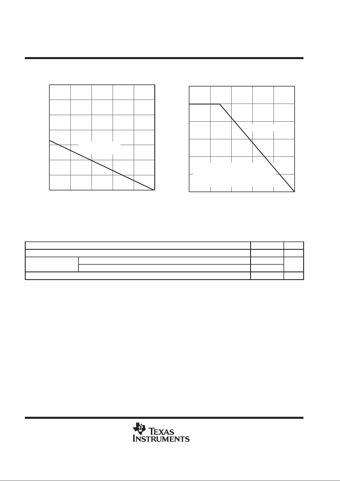
TPS60130, TPS60131, TPS60132, TPS60133
REGULATED 5-V, 300 mA HIGH EFFICIENCY CHARGE PUMP
DC/DC CONVERTERS
SLVS258A – NOVEMBER 1999 – REVISED DECEMBER 1999
12
POST OFFICE BOX 655303 • DALLAS, TEXAS 75265
TYPICAL CHARACTERISTICS
Figure 10
0
10
20
30
40
50
60
70
80
2.7 3.0 3.3 3.6 3.9 4.2 4.5 4.8 5.1 5.4
VI – Input Voltage – V
SUPPLY CURRENT
vs
INPUT VOLTAGE
Supply Current –
A
µ
IO = 0 mA
Figure 11
4.70
4.75
4.80
4.85
4.90
4.95
5.00
5.05
5.10
IO – Output Current – mA
TPS60132
OUTPUT VOLTAGE
vs
OUTPUT CURRENT
100.1 1 10 100 1000
VI = 5.4 V
VI = 2.7 V
VI = 3.6 V
V
O
–
O
u
t
pu
t
V
o
lt
age –
V
Figure 12
4.70
4.75
4.80
4.85
4.90
4.95
5.00
5.05
5.10
IO – Output Current – mA
TPS60132
OUTPUT VOLTAGE
vs
OUTPUT CURRENT
100.1 1 10 100 1000
VI = 5.4 V
VI = 2.7 V
VI = 3.6 V
V
O
– Output Voltage – V
Figure 13
V
O
– Output Voltage – V
VI – Input Voltage – V
4.84
4.86
4.88
4.90
4.92
4.94
4.96
4.98
5.00
2.7 3.0 3.3 3.6 3.9 4.2 4.5 4.8 5.1 5.4
IO = 1 mA
TPS60130
OUTPUT VOLTAGE
vs
INPUT VOLTAGE
IO = 150 mA
IO = 300 mA

TPS60130, TPS60131, TPS60132, TPS60133
REGULATED 5-V, 300 mA HIGH EFFICIENCY CHARGE PUMP
DC/DC CONVERTERS
SLVS258A – NOVEMBER 1999 – REVISED DECEMBER 1999
13
POST OFFICE BOX 655303 • DALLAS, TEXAS 75265
TYPICAL CHARACTERISTICS
Figure 14
V
O
– Output Voltage – V
4.90
4.91
4.92
4.93
4.94
4.95
4.96
4.97
4.98
4.99
5.00
2.7 3.2 3.7 4.2 4.7 5.2
VI – Input Voltage – V
TPS60132
OUTPUT VOLTAGE
vs
INPUT VOLTAGE
IO 1 mA
IO 75 mA
IO 150 mA
Figure 15
V
O
–
O
u
t
pu
t
V
o
lt
age –
V
4.950
4.955
4.960
4.965
4.970
4.975
4.980
4.985
4.990
4.995
5.000
0 50 100 150 200 250 300 350 400 450 500
OUTPUT VOLTAGE RIPPLE
vs
TIME
t – Time – µs
VI = 3.6 V
IO = 1 mA
Figure 16
4.90
4.92
4.94
4.96
4.98
5.00
5.02
02468101214161820
t – TIME – µs
OUTPUT VOLTAGE RIPPLE
vs
TIME
VI = 3.6 V
IO = 150 mA
V
O
– Output Voltage – V
Figure 17
4.95
4.96
4.97
4.98
4.99
5.00
5.01
5.02
5.03
5.04
5.05
0 2 4 6 8 10 12 14 16 18 20
t – TIME – µs
OUTPUT VOLTAGE RIPPLE
vs
TIME
VI = 3.6 V
IO = 300 mA
V
O
– Output Voltage – V

TPS60130, TPS60131, TPS60132, TPS60133
REGULATED 5-V, 300 mA HIGH EFFICIENCY CHARGE PUMP
DC/DC CONVERTERS
SLVS258A – NOVEMBER 1999 – REVISED DECEMBER 1999
14
POST OFFICE BOX 655303 • DALLAS, TEXAS 75265
TYPICAL CHARACTERISTICS
0
20
40
60
80
100
120
140
2.7 3.0 3.3 3.6 3.9 4.2 4.5 4.8 5.1 5.4
– Output Voltage Ripple Amplitude– mV
Figure 18
VI – Input Voltage – V
OUTPUT VOLTAGE RIPPLE AMPLITUDE
vs
INPUT VOLTAGE
IO = 150 mA
IO = 75 mA
IO = 1 mA
V
O
295
300
305
310
315
320
325
330
2.7 3.0 3.3 3.6 3.9 4.2 4.5 4.8 5.1 5.4
Figure 19
VI – Input Voltage – V
OSCILLATOR FREQUENCY
vs
INPUT VOLTAGE
T = –40 °C
T = 85 °C
T = 25 °C
f – Frequency – kHz
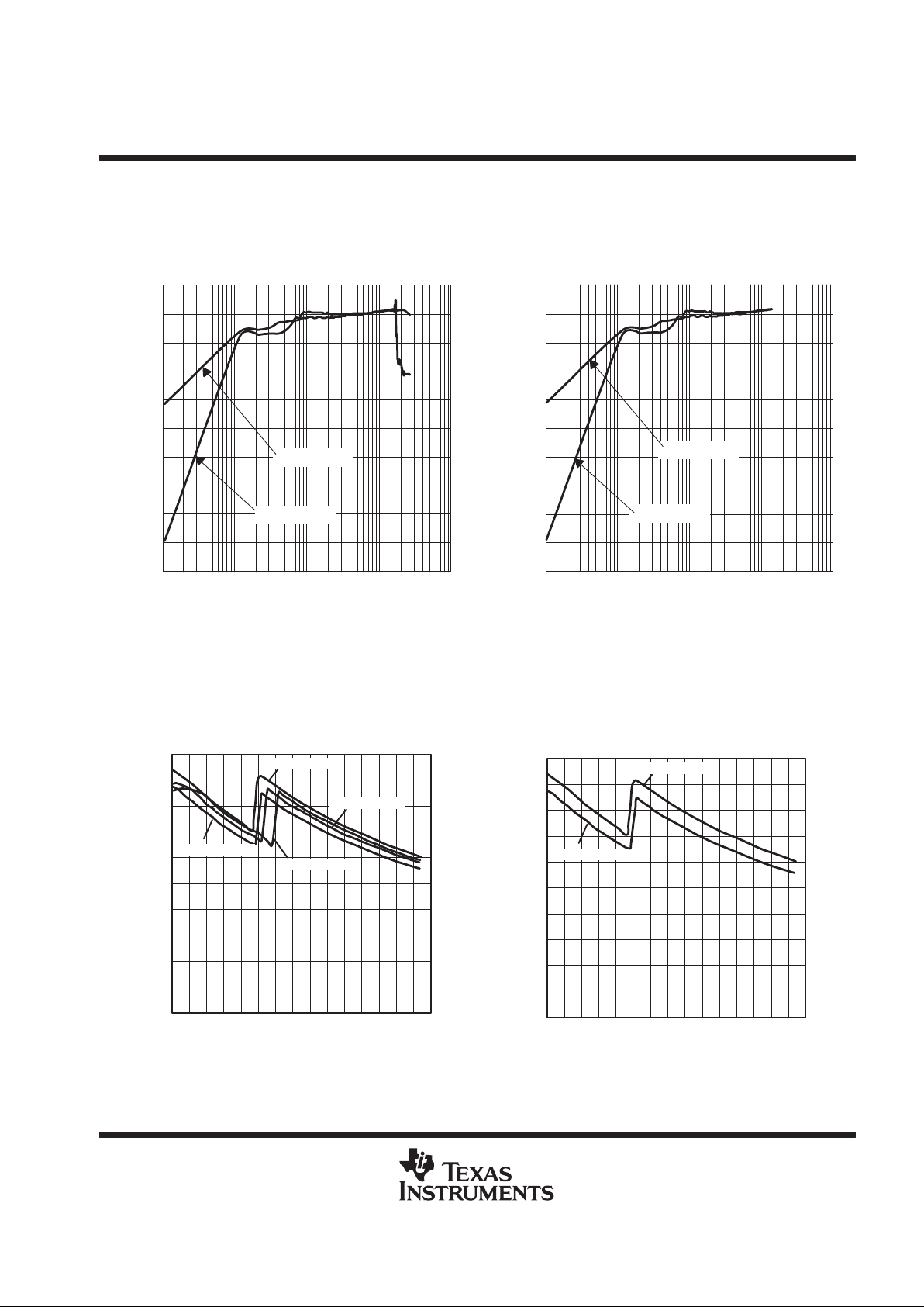
Figure 20
t – Time – ms
LOAD TRANSIENT RESPONSE
VI = 3.6 V
020
0
300
4.50
4.52
4.98
4.96
21816141210 46 8
I
O
V
O
– Output Voltage – V
– Output Current – mA
Figure 21
t – Time – ms
LINE TRANSIENT RESPONSE
IO = 150 mA
020
3.4
3.9
5.02
5.00
4.98
4.96
21816141210 46 8
V
I
V
O
– Output Voltage – V
– Input Voltage– V
TPS60130, TPS60131, TPS60132, TPS60133
REGULATED 5-V, 300 mA HIGH EFFICIENCY CHARGE PUMP
DC/DC CONVERTERS
SLVS258A – NOVEMBER 1999 – REVISED DECEMBER 1999
15
POST OFFICE BOX 655303 • DALLAS, TEXAS 75265
TYPICAL CHARACTERISTICS
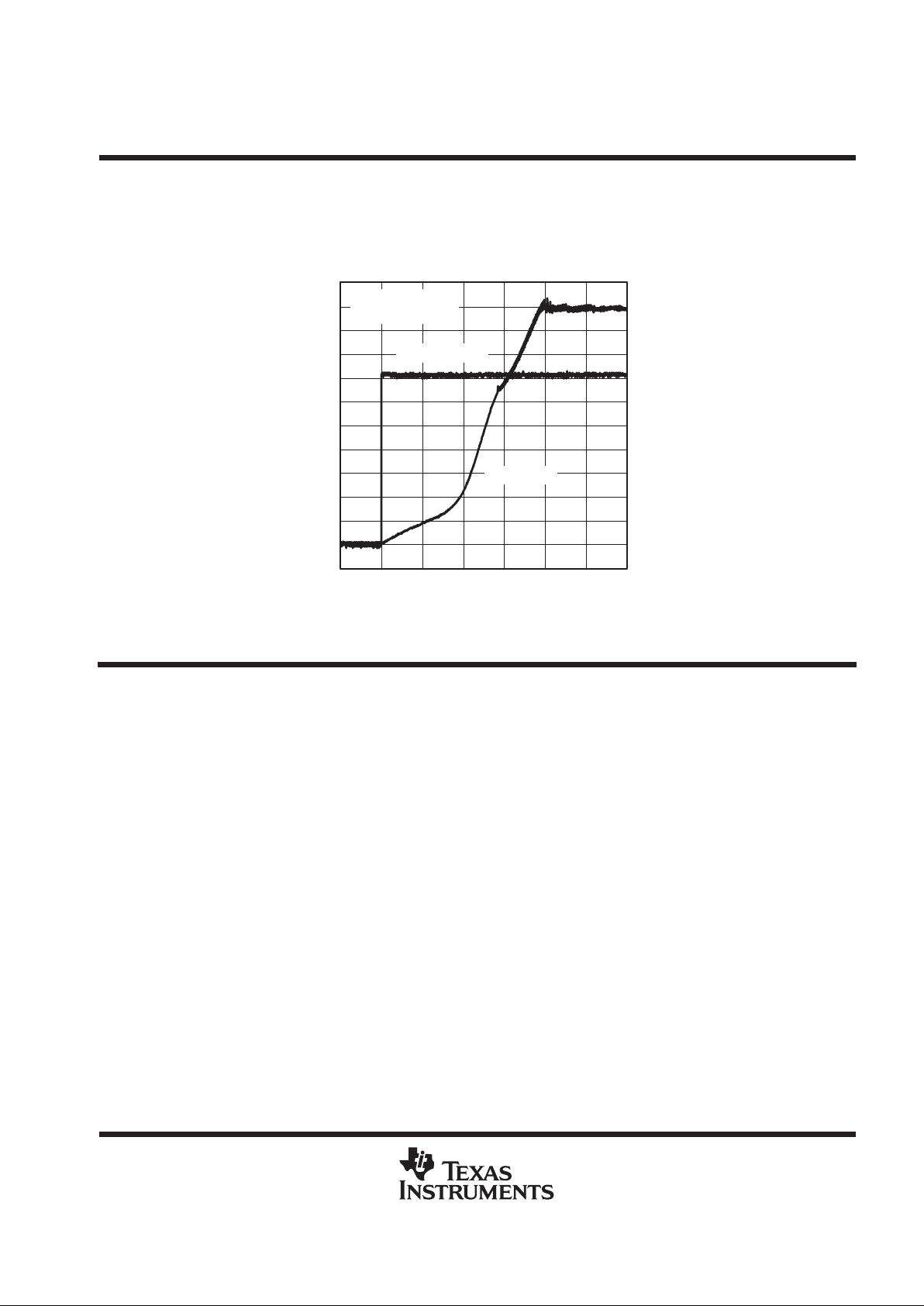
Figure 22
–0.5
0.0
0.5
1.0
1.5
2.0
2.5
3.0
3.5
4.0
4.5
5.0
5.5
–0.2 0.0 0.2 0.4 0.6 0.8 1.0 1.2
t – Time – ms
OUTPUT VOLTAGE
vs
TIME
(START-UP TIMING)
VO – V
VI = 3.6 V
R
LOAD
= 16.7 Ω
ENABLE – V
V
O
– Output Voltage and Enable – V
APPLICATION INFORMATION
capacitor selection
The TPS6013x charge pumps require only four external capacitors as shown in the basic application circuit.
Their capacitance values and types are closely linked to the output current and output noise/ripple
requirements. For lowest noise and ripple, low ESR (< 0.1 Ω) capacitors should be used for input and output
capacitors.
The input capacitor improves system efficiency by reducing the input impedance. It also stabilizes the input
current of the power source. The input capacitor should be chosen according to the power supply used and the
distance from power source to the converter IC. The input capacitor also has an impact on the output voltage
ripple. The lower the ESR of the input capacitor C
i
, the lower is the output ripple. Ci is recommended to be about
two to four times as large as C
(xF)
.
The output capacitor Co can be selected from 5-times to 50-times larger than C
(xF)
, depending on the ripple
tolerance. The larger C
o
, the lower will be the output voltage ripple. Ci and Co can be either ceramic or low-ESR
tantalum; aluminum capacitors are not recommended.
Generally, the flying capacitors C
(xF)
will be the smallest. Only ceramic capacitors are recommended, due to
their low ESR and because they retain their capacitance at the switching frequency. Because the device
regulates the output voltage using the pulse-skip technique, a larger flying capacitor will lead to a higher output
voltage ripple if the size of the output capacitor is not increased. Be aware that, depending on the material used
to manufacture them, ceramic capacitors might lose their capacitance over temperature. Ceramic capacitors
of type X7R or X5R material will keep their capacitance over temperature and voltage, whereas Z5U or Y5V-type
capacitors will decrease in capacitance. Table 2 lists recommended capacitor values.

TPS60130, TPS60131, TPS60132, TPS60133
REGULATED 5-V, 300 mA HIGH EFFICIENCY CHARGE PUMP
DC/DC CONVERTERS
SLVS258A – NOVEMBER 1999 – REVISED DECEMBER 1999
16
POST OFFICE BOX 655303 • DALLAS, TEXAS 75265
capacitor selection (continued)
Table 2. Recommended Capicator Values
V
I
C
i
(µF)
C
(xF)
(µF)
C
o
(µF)
V
PART
I
(V)O(mA)
TANTALUM
CERAMIC
(X7R)
(µ )
CERAMIC
(X7R)
TANTALUM
CERAMIC
(X7R)
PP(TYP)
(V)
22 4.7 90
225102.2
22 60
TPS60130
TPS60131
3.6
33 4.7 120
TPS60131
300 10 2.2
22 and 10 in
parallel
45
75 4.7 10
TPS60132
3.6
4.7 2.2
1
15 22 100
TPS60133
150
4.7 22 90
The TPS6013x devices are charge pumps that regulate the output voltage using pulse-skip regulation mode.
The output voltage ripple is therefore dependent on the values and the ESR of the input, output and flying
capacitors. The only possibility to reduce the output voltage ripple is to choose the appropriate capacitors. The
lowest output voltage ripple can be achieved using ceramic capacitors because of their low ESR and their
frequency characteristic.
Ceramic capacitors typically have an ESR that is more than 10 times lower than tantalum capacitors and they
retain their capacitance at frequencies more than 10 times higher than tantalum. Many different tantalum
capacitors act as an inductance for frequencies higher than 200 kHz. This behavior increases the output voltage
ripple. Therefore the best choice for a minimized ripple is the ceramic capacitor. For applications that do not
need a higher performance in output voltage ripple, tantalum capacitors with a low ESR are a possibility for input
and output capacitor, but a ceramic capacitor should be connected in parallel. Be aware that the ESR of tantalum
capacitors is indirectly proportional to the physical size of the capacitor.
Table 2 is a good starting point for choosing the capacitors. If the output voltage ripple is too high for the
application, it can be improved by selecting the appropriate capacitors. The first step is to increase the
capacitance at the output. If the ripple is still too high, the second step would be to increase the capacitance
at the input.
For the TPS60130 and TPS60131, the smallest board space can be achieved using Sprague’s 595D-series
tantalum capacitors for input and output. However, high capacitance ceramic capacitors will become
competitive in package size soon.
The smallest size for the lower-current devices TPS60132 and TPS60133 can be achieved using the suggested
ceramic capacitors.

TPS60130, TPS60131, TPS60132, TPS60133
REGULATED 5-V, 300 mA HIGH EFFICIENCY CHARGE PUMP
DC/DC CONVERTERS
SLVS258A – NOVEMBER 1999 – REVISED DECEMBER 1999
17
POST OFFICE BOX 655303 • DALLAS, TEXAS 75265
APPLICATION INFORMATION
capacitor selection (continued)
Tables 3 and 4 lists the manufacturers of recommended capacitors. In most applications surface-mount
tantalum capacitors will be the right choice. However, ceramic capacitors provide the lowest output voltage
ripple due to their typically lower ESR.
Table 3. Recommended Capacitors
MANUFACTURER PART NUMBER CAPACITANCE CASE SIZE TYPE
Taiyo Yuden
LMK212BJ105KG–T 1 µF 0805 Ceramic
LMK212BJ225MG–T 2.2 µF 0805 Ceramic
LMK316BJ475KL–T 4.7 µF 1206 Ceramic
LMK325BJ106MN–T 10 µF 1210 Ceramic
LMK432BJ226MM–T 22 µF 1812 Ceramic
AVX
0805ZC105KAT2A 1 µF 0805 Ceramic
1206ZC225KAT2A 2.2 µF 1206 Ceramic
TPSC475035R0600 4.7 µF Case C Tantalum
TPSC156025R0500 15 µF Case C Tantalum
TPSC336010R0375 33 µF Case C Tantalum
Sprague
595D156X0016B2T 15 µF Case B T antalum
595D226X0016B2T 22 µF Case B T antalum
595D336X0016B2T 33 µF Case B T antalum
595D336X0016C2T 33 µF Case C Tantalum
Kemet
T494C156K010AS 15 µF Case C Tantalum
T494C226K010AS 22 µF Case C Tantalum
T494C336K010AS 33 µF Case C Tantalum
NOTE: Case code compatibility with EIA 535BAAC and CECC30801 molded chips.
Table 4. Recommended Capacitor Manufacturers
MANUFACTURER CAPACITOR TYPE INTERNET SITE
Taiyo Yuden X7R/X5R ceramic http://www.t–yuden.com/
AVX X7R/X5R ceramic
TPS-series tantalum
http://www.avxcorp.com/
Sprague 595D-series tantalum
593D-series tantalum
http://www.vishay.com/
Kemet T494-series tantalum http://www.kemet.com/
power dissipation
The power dissipated in the TPS6013x depends on output current and the mode of operation (1.5x or doubler
voltage conversion mode). It is described by the following equation:
P
DISS
=
ǒ
1
h
–
1
Ǔ
V
O
× IO (Efficiency η mainly depends on VI and also on IO. See efficiency graphs.)
P
DISS
must be less than that allowed by the package rating. See the absolute maximum ratings for 20-pin PWP
package power-dissipation limits and deratings.

TPS60130, TPS60131, TPS60132, TPS60133
REGULATED 5-V, 300 mA HIGH EFFICIENCY CHARGE PUMP
DC/DC CONVERTERS
SLVS258A – NOVEMBER 1999 – REVISED DECEMBER 1999
18
POST OFFICE BOX 655303 • DALLAS, TEXAS 75265
APPLICATION INFORMATION
board layout
Careful board layout is necessary due to the high transient currents and switching frequency of the converter.
All capacitors should be soldered in close proximity to the IC. Connect ground and power ground pins through
a short, low-impedance trace. A PCB layout proposal for a two-layer board is given in Figure 23. The bottom
layer of the board carries only ground potential for best performance. The layout also provides improved thermal
performance as the exposed lead frame is soldered to the PCB.
An evaluation module for the TPS60130 is available and can be ordered under product code
TPS60130EVM-143. The EVM uses the layout shown in Figure 23.
Figure 23. Recommended PCB Layout for
TPS6013X
Figure 24. Component Placement for
TPS6013X EVM
Table 5. Component Identification
IC1 TPS6013x
C1, C2 Flying capacitors
C3, C6 Input capacitors
C4, C5 Onput capacitors
C7 Stabilization capacitor for LBI
R1, R2 Resistive divider for LBI
R3 Pullup resistor for LBO
The best performance of the converter is achieved with the additional bypass capacitors C5 and C6 at input and
output. Capacitor C7 should be included if the large line transients are expected. The capacitors are not
required. They can be omitted in most applications.

TPS60130, TPS60131, TPS60132, TPS60133
REGULATED 5-V, 300 mA HIGH EFFICIENCY CHARGE PUMP
DC/DC CONVERTERS
SLVS258A – NOVEMBER 1999 – REVISED DECEMBER 1999
19
POST OFFICE BOX 655303 • DALLAS, TEXAS 75265
APPLICATION INFORMATION
application proposals
paralleling of two TPS6013x to deliver 600 mA total output current
Two TPS60130x devices can be connected in parallel to yield higher load currents. The circuit of Figure 25 can
deliver up to 600 mA at an output voltage of 5 V. The devices can share the output capacitors, but each one
requires its own transfer capacitors and input capacitor. If both a TPS60130 and a TPS60131 are used, it is
possible to monitor the battery voltage with the TPS60130 using the low-battery comparator function and to
supervise the output voltage with the TPS60131 using the power-good comparator. Make the layout of the
charge pumps as similar as possible, and position the output capacitor the same distance from both devices.
IN
IN
LBI
C1+
C1–
ENABLE
PGND GND
OUT
OUT
FB
LBO
C2+
C2–
C
o
47 µF
Ci
15 µF
Output
5 V, 600 mA
C2
2.2 µF
C1
2.2 µF
R1
562 kΩ
R2
453 kΩ
Input
2.7 V to 5.4 V
Off/On
IN
IN
NC
C1+
C1–
ENABLE
PGND GND
OUT
OUT
FB
PG
C2+
C2–
C2
2.2 µF
C1
2.2 µF
C
i
15 µF
R3
1 MΩ
Low Battery
Warning
Power-Good
Signal
R4
1 MΩ
TPS60130 TPS60131
Figure 25. Paralleling of Two TPS6013x Charge Pumps

TPS60130, TPS60131, TPS60132, TPS60133
REGULATED 5-V, 300 mA HIGH EFFICIENCY CHARGE PUMP
DC/DC CONVERTERS
SLVS258A – NOVEMBER 1999 – REVISED DECEMBER 1999
20
POST OFFICE BOX 655303 • DALLAS, TEXAS 75265
APPLICATION INFORMATION
TPS6013x operated with ultra-low quiescent current
Because the output of the TPS6013x is isolated from the input when the devices are disabled, and because the
internal resistive divider is disconnected in shutdown, an ultra-low quiescent current mode can be implemented.
In this mode, the output voltage is sustained because the converter is periodically enabled to refresh the output
capacitor. The necessary external control signal that is applied to the ENABLE-pin is generated from a
microcontroller. For a necessary supply current for the system of 1 mA and a minimum supply voltage of 4.5
V with a 33-µF output capacitor, the refresh has to be done after 9 ms. Longer refresh periods can be achieved
with a larger output capacitor.
IN
IN
LBI
C1+
C1–
ENABLE
PGND GND
OUT
OUT
FB
LBO
C2+
C2–
C2
33 µF
C
i
15 µF
Output
5 V , 150 mA
C2
2.2 µF
C1
2.2 µF
R1
R2
Input
2.7 V to 5.4 V
ON
OFF
C3
1 µF
R4
1 MΩ
R3
1 MΩ
I
O
µC
TPS60132
Figure 26. TPS60132 in Ultra-Low Quiescent Current Mode
regulated discharge of the output capacitors after disabling of the TPS6013x
During shutdown of the charge pump TPS6013x the output is isolated from the input. Therefore the discharging
of the output capacitor depends on the load and on the leakage current of the capacitor. In certain applications
it is necessary to completely remove the supply voltage from the load in shutdown mode. That means the output
capacitor of the charge pump has to be actively discharged when the charge pump is disabled. Figure 10 shows
one solution to this problem.
TPS601xx
OUT
IN
GND
ENABLE
+
C
O
SN74AHC1G04
A
Y
VCC
GND
IN
ENABLE
GND
OUT
BSS138
Figure 27. Block Diagram of the Regulated Discharge of the Output Capacitor

TPS60130, TPS60131, TPS60132, TPS60133
REGULATED 5-V, 300 mA HIGH EFFICIENCY CHARGE PUMP
DC/DC CONVERTERS
SLVS258A – NOVEMBER 1999 – REVISED DECEMBER 1999
21
POST OFFICE BOX 655303 • DALLAS, TEXAS 75265
APPLICATION INFORMATION
related information
application reports
For more application information see:
D
PowerPAD Application Report, Literature Number SLMA002
D
TPS6010x/TPS6011x Charge Pump Application Report
, Literature Number SLVA070
D
Powering the TMS320C5420 Using the TPS60100, TPS76918, and the TPS3305-18, Literature Number
SLV A082.
device family products
Other devices in this family are:
PART NUMBER
DATASHEET
LITERATURE
CODE
DESCRIPTION
TPS60100 SLVS213B Regulated 3.3-V, 200-mA low-noise charge pump dc-dc converter
TPS60101 SL VS214A Regulated 3.3-V, 100-mA low-noise charge pump dc-dc converter
TPS60110 SLVS215A Regulated 5-V, 300-mA low-noise charge pump dc-dc converter
TPS60111 SLVS216A Regulated 5-V , 150-mA low-noise charge pump dc-dc converter
TPS60120 SLVS257 Regulated 3.3-V , 200-mA high ef ficiency charge pump dc-dc converter with low-battery comparator
TPS60121 SLVS257 Regulated 3.3-V , 200-mA high efficiency charge pump dc-dc converter with power-good comparator
TPS60122 SLVS257 Regulated 3.3-V , 100-mA high ef ficiency charge pump dc-dc converter with low-battery comparator
TPS60123 SLVS257 Regulated 3.3-V , 100-mA high efficiency charge pump dc-dc converter with power-good comparator

TPS60130, TPS60131, TPS60132, TPS60133
REGULATED 5-V, 300 mA HIGH EFFICIENCY CHARGE PUMP
DC/DC CONVERTERS
SLVS258A – NOVEMBER 1999 – REVISED DECEMBER 1999
22
POST OFFICE BOX 655303 • DALLAS, TEXAS 75265
MECHANICAL DATA
PWP (R-PDSO-G**) PowerPAD PLASTIC SMALL-OUTLINE
4073225/F 10/98
0,50
0,75
0,25
0,15 NOM
Thermal Pad
(See Note D)
Gage Plane
2824
7,70
7,90
20
6,40
6,60
9,60
9,80
6,60
6,20
11
0,19
4,50
4,30
10
0,15
20
A
1
0,30
1,20 MAX
1614
5,10
4,90
PINS **
4,90
5,10
DIM
A MIN
A MAX
0,05
Seating Plane
0,65
0,10
M
0,10
0°–8°
20 PINS SHOWN
NOTES: A. All linear dimensions are in millimeters.
B. This drawing is subject to change without notice.
C. Body dimensions do not include mold flash or protrusions.
D. The package thermal performance may be enhanced by bonding the thermal pad to an external thermal plane.
This pad is electrically and thermally connected to the backside of the die and possibly selected leads.
E. Falls within JEDEC MO-153
PowerPAD is a trademark of Texas Instruments Incorporated.

IMPORTANT NOTICE
T exas Instruments and its subsidiaries (TI) reserve the right to make changes to their products or to discontinue
any product or service without notice, and advise customers to obtain the latest version of relevant information
to verify, before placing orders, that information being relied on is current and complete. All products are sold
subject to the terms and conditions of sale supplied at the time of order acknowledgement, including those
pertaining to warranty, patent infringement, and limitation of liability.
TI warrants performance of its semiconductor products to the specifications applicable at the time of sale in
accordance with TI’s standard warranty. Testing and other quality control techniques are utilized to the extent
TI deems necessary to support this warranty. Specific testing of all parameters of each device is not necessarily
performed, except those mandated by government requirements.
CERT AIN APPLICATIONS USING SEMICONDUCTOR PRODUCTS MAY INVOLVE POTENTIAL RISKS OF
DEATH, PERSONAL INJURY, OR SEVERE PROPERTY OR ENVIRONMENTAL DAMAGE (“CRITICAL
APPLICATIONS”). TI SEMICONDUCTOR PRODUCTS ARE NOT DESIGNED, AUTHORIZED, OR
WARRANTED TO BE SUITABLE FOR USE IN LIFE-SUPPORT DEVICES OR SYSTEMS OR OTHER
CRITICAL APPLICATIONS. INCLUSION OF TI PRODUCTS IN SUCH APPLICA TIONS IS UNDERSTOOD T O
BE FULLY AT THE CUSTOMER’S RISK.
In order to minimize risks associated with the customer’s applications, adequate design and operating
safeguards must be provided by the customer to minimize inherent or procedural hazards.
TI assumes no liability for applications assistance or customer product design. TI does not warrant or represent
that any license, either express or implied, is granted under any patent right, copyright, mask work right, or other
intellectual property right of TI covering or relating to any combination, machine, or process in which such
semiconductor products or services might be or are used. TI’s publication of information regarding any third
party’s products or services does not constitute TI’s approval, warranty or endorsement thereof.
Copyright 1999, Texas Instruments Incorporated
 Loading...