

Page 1

User's Guide
SLVU954–September 2013
TPS560200EVM-537 0.5-A, Single Channel Regulator
Evaluation Module
This user's guide contains information for the TPS560200 as well as support documentation for the
TPS560200EVM-537 evaluation module. Included are the performance specifications, schematic, and the
bill of materials of the TPS560200EVM-537.
Contents
1 Introduction .................................................................................................................. 2
2 Performance Specification Summary ..................................................................................... 2
3 Modifications ................................................................................................................. 3
3.1 Output Voltage Setpoint ........................................................................................... 3
4 Test Setup and Results .................................................................................................... 4
4.1 Input/Output Connections ......................................................................................... 4
4.2 Start-Up Procedure ................................................................................................ 4
4.3 Efficiency ............................................................................................................ 5
4.4 Load Regulation .................................................................................................... 6
4.5 Line Regulation ..................................................................................................... 6
4.6 Load Transient Response ........................................................................................ 7
4.7 Output Voltage Ripple ............................................................................................. 8
4.8 Input Voltage Ripple ............................................................................................... 9
4.9 Start-Up ............................................................................................................ 10
4.10 Shut-Down ......................................................................................................... 11
5 Board Layout ............................................................................................................... 12
5.1 Layout .............................................................................................................. 12
6 Schematic, Bill of Materials, and Reference ........................................................................... 15
6.1 Schematic ......................................................................................................... 15
6.2 Bill of Materials .................................................................................................... 16
6.3 Reference .......................................................................................................... 16
1 TPS560200EVM-537 Efficiency........................................................................................... 5
2 TPS560200EVM-537 Light Load Efficiency ............................................................................. 5
3 TPS560200EVM-537 Load Regulation .................................................................................. 6
4 TPS560200EVM-537 Line Regulation ................................................................................... 6
5 TPS560200EVM-537 Load Transient Response, 25% to 75% Load Step.......................................... 7
6 TPS560200EVM-537 Load Transient Response, No Load to 50% Load Step..................................... 7
7 TPS560200EVM-537 Output Voltage Ripple, I
8 TPS560200EVM-537 Output Voltage Ripple, I
9 TPS560200EVM-537 Output Voltage Ripple, I
10 TPS560200EVM-537 Input Voltage Ripple, I
11 TPS560200EVM-537 Start-Up Relative to V
12 TPS560200EVM-537 Start-Up Relative to EN ........................................................................ 10
13 TPS560200EVM-537 Shut-Down Relative to V
14 TPS560200EVM-537 Shut-Down Relative to EN ..................................................................... 11
D-CAP2, SWIFT, Eco-mode are trademarks of Texas Instruments.
SLVU954–September 2013 TPS560200EVM-537 0.5-A, Single Channel Regulator Evaluation Module
Submit Documentation Feedback
List of Figures
= 0.5 A............................................................. 8
OUT
= 30 mA ........................................................... 8
OUT
= 0 A............................................................... 9
OUT
= 0.5 A............................................................... 9
OUT
......................................................................... 10
IN
...................................................................... 11
IN
Copyright © 2013, Texas Instruments Incorporated
1
Page 2
Introduction
15 Top Assembly.............................................................................................................. 12
16 Top Layer................................................................................................................... 13
17 Bottom Layer............................................................................................................... 14
18 TPS560200EVM-537Schematic Diagram.............................................................................. 15
1 Input Voltage and Output Current Summary ............................................................................ 2
2 TPS560200EVM-537Performance Specifications Summary.......................................................... 2
3 Output Voltages............................................................................................................. 3
4 Connection and Test Points ............................................................................................... 4
5 Bill of Materials............................................................................................................. 16
1 Introduction
The TPS560200 is a single, adaptive on-time, D-CAP2™-mode, synchronous buck converter requiring a
very low external component count. The D-CAP2 control circuit is optimized for low-ESR output capacitors
such as POSCAP, SP-CAP, or ceramic types and features fast transient response with no external
compensation. The switching frequency is internally set at a nominal 600 kHz. The high-side and low-side
switching MOSFETs are incorporated inside the TPS560200 package along with the gate-drive circuitry.
The low drain-to-source on resistance of the MOSFETs allows the TPS560200 to achieve high efficiencies
and helps keep the junction temperature low at high output currents. The TPS560200 dc/dc synchronous
converter is designed to provide up to a 0.5-A output from an input voltage source of 4.5 V to 17 V. The
output voltage range is from 0.8 V to 5.5 V. Rated input voltage and output current ranges for the
evaluation module are given in Table 1.
The TPS560200EVM-537 evaluation module (EVM) is a single, synchronous buck converter providing
1.05 V at 0.5 A from 4.5-V to 17-V input. This user’s guide describes the TPS560200EVM-537
performance.
www.ti.com
List of Tables
Table 1. Input Voltage and Output Current Summary
EVM Input Voltage Range Output Current Range
TPS560200EVM-537 VIN= 4.5 V to 17 V 0 A to 0.5 A
2 Performance Specification Summary
A summary of the TPS560200EVM-537 performance specifications is provided in Table 2. Specifications
are given for an input voltage of VIN= 12 V and an output voltage of 1.05 V, unless otherwise noted. The
ambient temperature is 25°C for all measurement, unless otherwise noted.
Table 2. TPS560200EVM-537Performance Specifications Summary
Specifications Test Conditions Min Typ Max Unit
Input voltage range (VIN) 4.5 12 17 V
Output voltage 1.05 V
Operating frequency VIN= 12 V, IO= 0.5 A 600 kHz
CH1 Output current range 0 0.5 A
Over current limit VIN= 12 V, LO= 10 µH 0.55 A
Output ripple voltage VIN= 12 V, IO= 0.5 A 10 mV
PP
2
TPS560200EVM-537 0.5-A, Single Channel Regulator Evaluation Module SLVU954–September 2013
Copyright © 2013, Texas Instruments Incorporated
Submit Documentation Feedback
Page 3
OUT
R1 0.8 V
V -0.8V
´
www.ti.com
3 Modifications
These evaluation modules are designed to provide access to the features of the TPS560200. Some
modifications can be made to this module.
3.1 Output Voltage Setpoint
To change the output voltage of the EVMs, it is necessary to change the value of resistor R1. Changing
the value of R1 can change the output voltage above 0.765 V. The value of R1 for a specific output
voltage can be calculated using Equation 1.
Table 3 lists the R1 values for some common output voltages. For higher output voltages of 1.8 V or
above, a feedforward capacitor (C3) may be required to improve phase margin. Pads for this component
(C3) are provided on the printed-circuit board. Note that the values given in Table 3 are standard values
and not the exact value calculated using Table 3.
Modifications
(1)
Table 3. Output Voltages
Output Voltage R1 R2 C3 C4 + C5
(V) (kΩ) (kΩ) (pF) (µF)
1.0 6.19 20.0 10 10 + 10
1.05 6.19 20.0 10 10 + 10
1.2 10.0 20.0 10 10 + 10
1.5 17.4 20.0 10 10 + 10
1.8 24.9 20.0 optional 10 10 + 10
2.5 42.2 20.0 optional 10 10 + 10
3.3 61.9 20.0 optional 10 10 + 10
5.0 105 20.0 optional 10 10 + 10
Min Typ Max
L1
(µH)
SLVU954–September 2013 TPS560200EVM-537 0.5-A, Single Channel Regulator Evaluation Module
Submit Documentation Feedback
3
Copyright © 2013, Texas Instruments Incorporated
Page 4
Test Setup and Results
4 Test Setup and Results
This section describes how to properly connect, set up, and use the TPS560200EVM-537. The section
also includes test results typical for the evaluation modules and efficiency, output load regulation, output
line regulation, load transient response, output voltage ripple, input voltage ripple, start-up, and switching
frequency.
4.1 Input/Output Connections
The TPS560200EVM-537 is provided with input/output connectors and test points as shown in Table 4. A
power supply capable of supplying 2 A must be connected to J1 through a pair of 20-AWG wires. The load
must be connected to J2 through a pair of 20-AWG wires. The maximum load current capability is 1 A.
Wire lengths must be minimized to reduce losses in the wires. Test point TP1 provides a place to monitor
the VINinput voltages with TP2 providing a convenient ground reference. TP7 is used to monitor the output
voltage with TP8 as the ground reference.
Reference Designator Function
J1-1 VINpositive sense and monitor point
J1-2 VIN(see Table 1 for VINrange)
J2-1 Ground return for V
J2-2 VINnegative sense and monitor point
J3-1 V
J3-2 V
J4-1 Ground return for V
J4-2 V
JP1 EN control. Shunt EN to GND to disable, open EN to enable.
TP1 Switch node test point
TP2 Test point for loop response measurements
Table 4. Connection and Test Points
positive sense and monitor point
OUT
, 1.05 V at 0.5-A maximum
OUT
negative sense and monitor point
OUT
www.ti.com
IN
OUT
4.2 Start-Up Procedure
1. Ensure that the jumper at JP1 (Enable control) is covered to shunt EN to GND, disabling the output.
2. Apply appropriate VINvoltage to VI (J1-2) and GND (J2-1).
3. Remove the jumper at JP1 (Enable control) to uncover EN and GND, enabling the output.
4
TPS560200EVM-537 0.5-A, Single Channel Regulator Evaluation Module SLVU954–September 2013
Copyright © 2013, Texas Instruments Incorporated
Submit Documentation Feedback
Page 5
0
10
20
30
40
50
60
70
80
90
100
0.001 0.01 0.1 1
Efficiency - %
Output Current - A
C002
VIN = 5 V
VIN = 12 V
0
10
20
30
40
50
60
70
80
90
0.00 0.05 0.10 0.15 0.20 0.25 0.30 0.35 0.40 0.45 0.50
Efficiency - %
Output Current - A
C001
VIN = 5 V
VIN = 12 V
www.ti.com
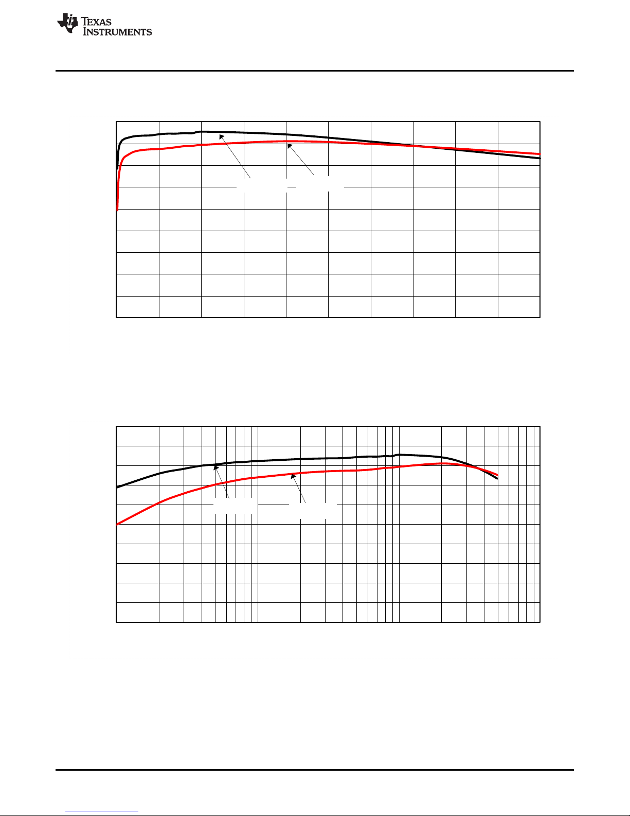
4.3 Efficiency
Figure 1 shows the efficiency for the TPS560200EVM-537 at an ambient temperature of 25°C.
Test Setup and Results
Figure 2 shows the efficiency at light loads for the TPS560200EVM-537 at an ambient temperature of
25°C.
SLVU954–September 2013 TPS560200EVM-537 0.5-A, Single Channel Regulator Evaluation Module
Submit Documentation Feedback
Figure 2. TPS560200EVM-537 Light Load Efficiency
Figure 1. TPS560200EVM-537 Efficiency
5
Copyright © 2013, Texas Instruments Incorporated
Page 6
-0.5
-0.4
-0.3
-0.2
-0.1
0
0.1
0.2
0.3
0.4
0.5
4 6 8 10 12 14 16 18
Line Rgulation - %
Input Voltage - V
C004
I
OUT
= 0.25 A
±1.50
±1.00
±0.50
0.00
0.50
1.00
1.50
0.00 0.05 0.10 0.15 0.20 0.25 0.30 0.35 0.40 0.45 0.50
Load Regulation - %
Output Current - A
C003
VIN = 5 V
VIN = 12 V
Test Setup and Results
4.4 Load Regulation
The load regulation for the TPS560200EVM-537 is shown in Figure 3.
www.ti.com
4.5 Line Regulation
The line regulation for the TPS560200EVM-537 is shown in Figure 4.
Figure 3. TPS560200EVM-537 Load Regulation
6
TPS560200EVM-537 0.5-A, Single Channel Regulator Evaluation Module SLVU954–September 2013
Figure 4. TPS560200EVM-537 Line Regulation
Copyright © 2013, Texas Instruments Incorporated
Submit Documentation Feedback
Page 7

V = 50 mV / div (ac coupled)
OUT
Time = 200 µsec / div
I = 200 mA / div
OUT
Load step = 10 mA - 250 mA, slew rate = 500 mA / µsec
V = 50 mV / div (ac coupled)
OUT
Time = 200 µsec / div
I = 200 mA / div
OUT
Load step = 125 mA - 375 mA, slew rate = 500 mA / µsec
www.ti.com
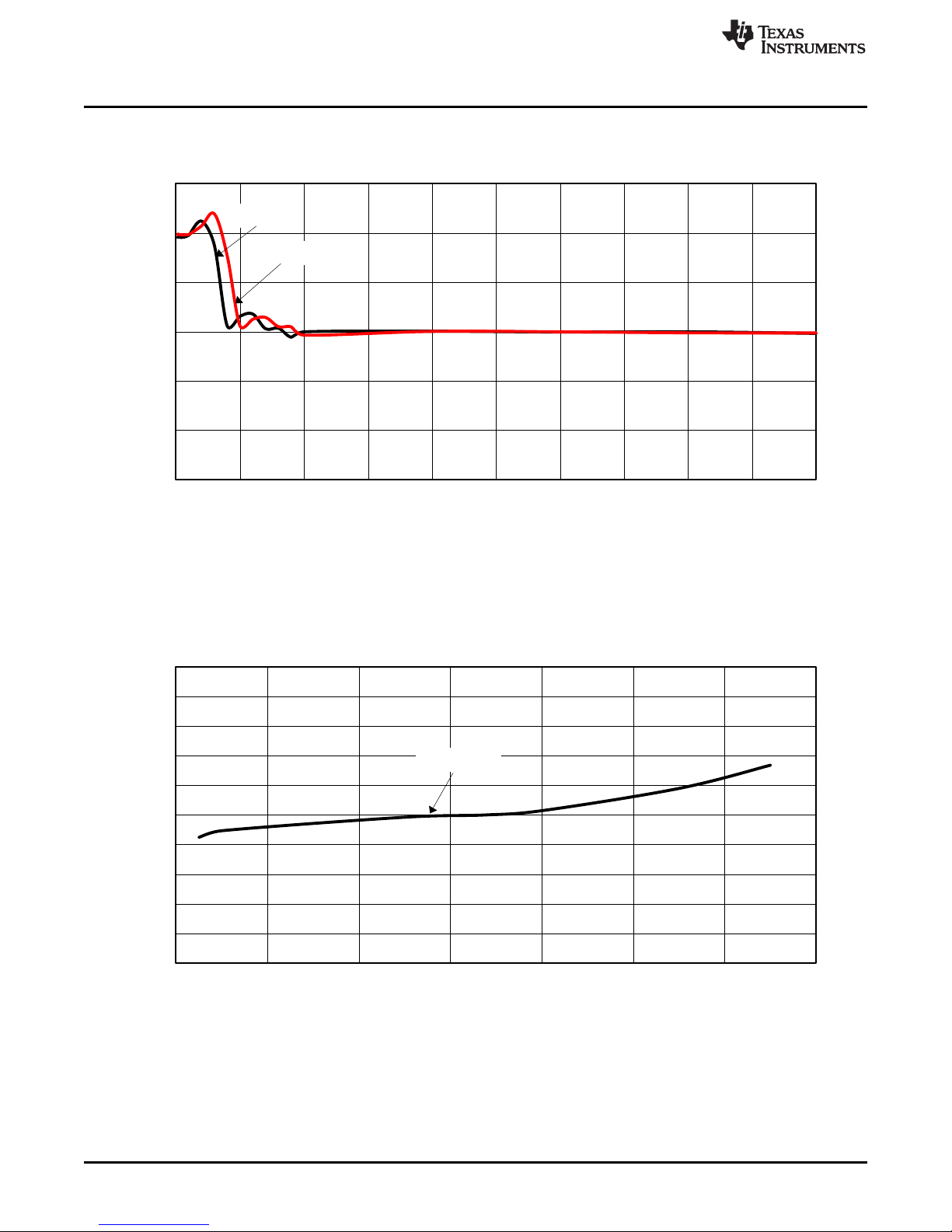
4.6 Load Transient Response
The TPS560200EVM-537 response to load transient is shown in Figure 5 and Figure 6. The current steps
and slew rates are indicated in the figures. Total peak-to-peak voltage variation is as shown.
Test Setup and Results
Figure 5. TPS560200EVM-537 Load Transient Response, 25% to 75% Load Step
Figure 6. TPS560200EVM-537 Load Transient Response, No Load to 50% Load Step
SLVU954–September 2013 TPS560200EVM-537 0.5-A, Single Channel Regulator Evaluation Module
Submit Documentation Feedback
7
Copyright © 2013, Texas Instruments Incorporated
Page 8
V = 20 mV / div (ac coupled)
OUT
Time = 5 µsec / div
SW = 5 V / div
V = 20 mV / div (ac coupled)
OUT
Time = 1 µsec / div
SW = 5 V / div
Test Setup and Results
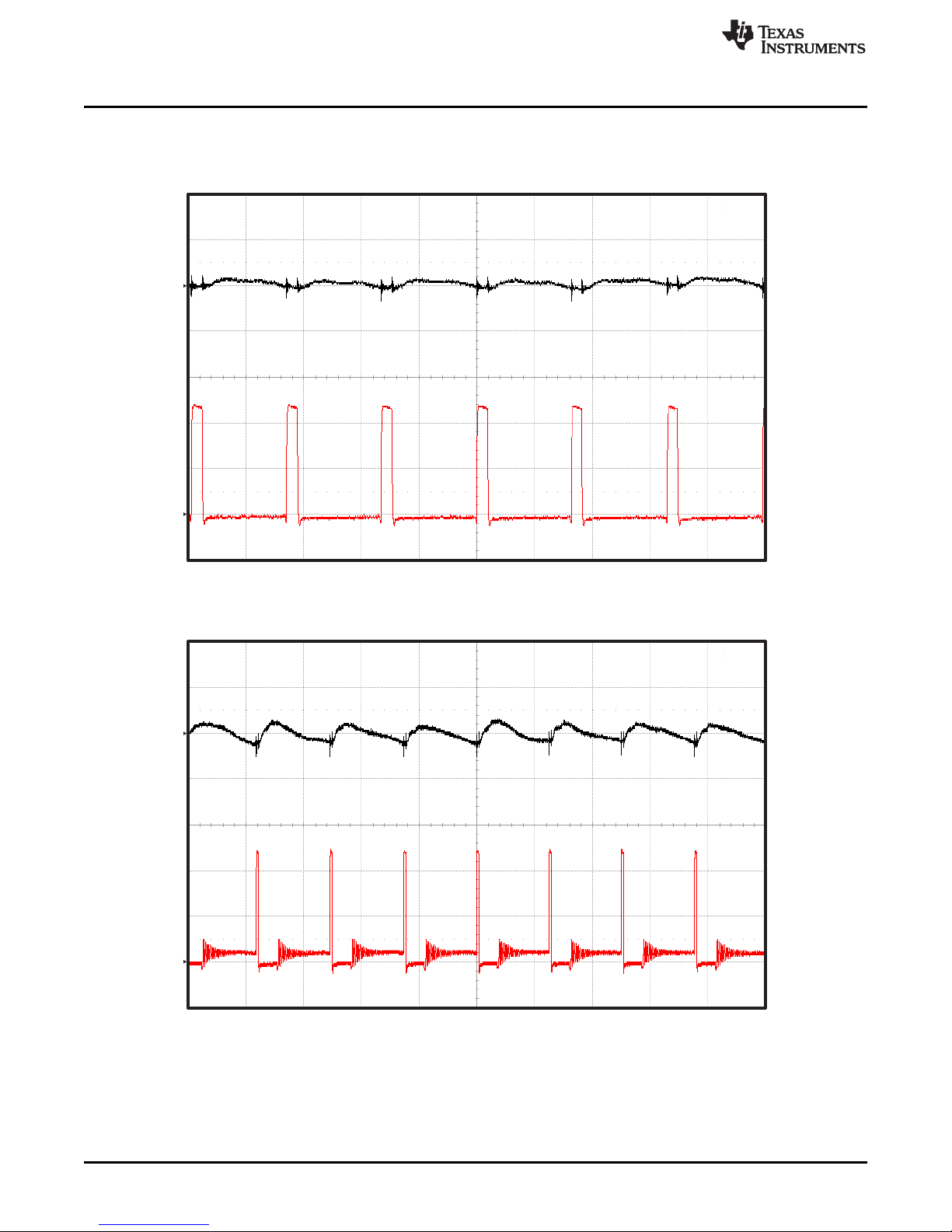
4.7 Output Voltage Ripple
The TPS560200EVM-537 output voltage ripple is shown in Figure 7, Figure 8, and Figure 9. The output
currents are as indicated.
www.ti.com
Figure 7. TPS560200EVM-537 Output Voltage Ripple, I
Figure 8. TPS560200EVM-537 Output Voltage Ripple, I
OUT
= 30 mA
OUT
= 0.5 A
8
TPS560200EVM-537 0.5-A, Single Channel Regulator Evaluation Module SLVU954–September 2013
Copyright © 2013, Texas Instruments Incorporated
Submit Documentation Feedback
Page 9
V = 20 mV / div (ac coupled)
IN
Time = 1 µsec / div
SW = 5 V / div
V = 20 mV / div (ac coupled)
OUT
Time = 2 msec / div
SW = 5 V / div
www.ti.com
Test Setup and Results
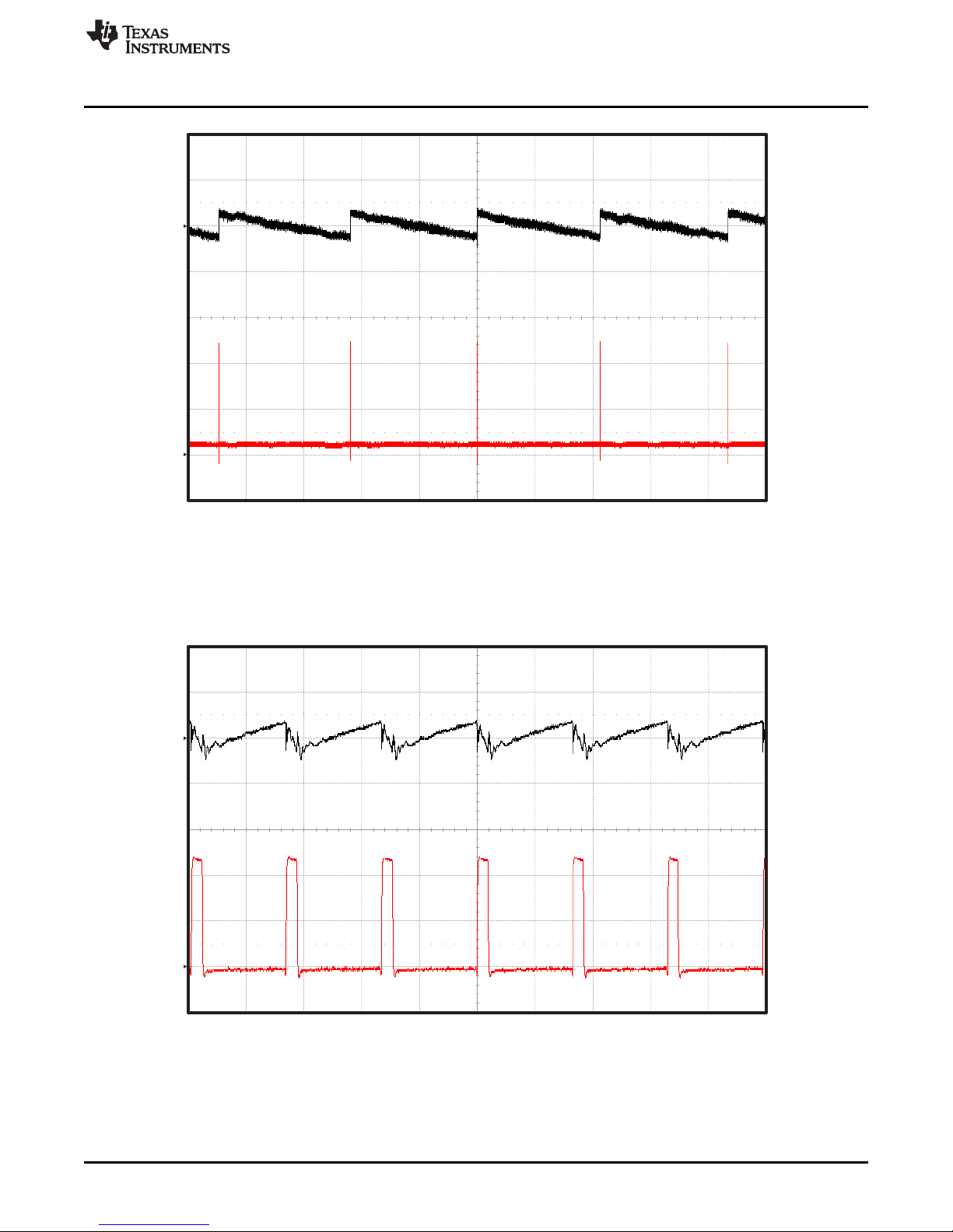
4.8 Input Voltage Ripple
The TPS560200EVM-537 input voltage ripple is shown in Figure 10. The output current is as indicated.
Figure 9. TPS560200EVM-537 Output Voltage Ripple, I
OUT
= 0 A
Figure 10. TPS560200EVM-537 Input Voltage Ripple, I
SLVU954–September 2013 TPS560200EVM-537 0.5-A, Single Channel Regulator Evaluation Module
Submit Documentation Feedback
Copyright © 2013, Texas Instruments Incorporated
OUT
= 0.5 A
9
Page 10
V = 500 mV / div
OUT
Time = 2 msec / div
EN = 5 V / div
V = 5 V / div
IN
V = 500 mV / div
OUT
Time = 2 msec / div
EN = 5 V / div
V = 5 V / div
IN
Test Setup and Results
4.9 Start-Up
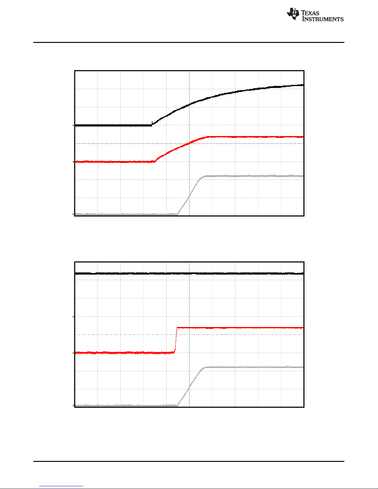
The TPS560200EVM-537 start-up waveform relative to VINis shown in Figure 11. Load = 4 Ω resistive.
www.ti.com
Figure 11. TPS560200EVM-537 Start-Up Relative to V
IN
The TPS560200EVM-537 start-up waveform relative to enable (EN) is shown in Figure 12. Load = 4 Ω
resistive.
10
TPS560200EVM-537 0.5-A, Single Channel Regulator Evaluation Module SLVU954–September 2013
Figure 12. TPS560200EVM-537 Start-Up Relative to EN
Copyright © 2013, Texas Instruments Incorporated
Submit Documentation Feedback
Page 11

V = 500 mV / div
OUT
Time = 2 msec / div
EN = 5 V / div
V = 5 V / div
IN
V = 500 mV / div
OUT
Time = 2 msec / div
EN = 5 V / div
V = 5 V / div
IN
www.ti.com
4.10 Shut-Down
The TPS560200EVM-537 shut-down waveform relative to VINis shown in Figure 13. Load = 4 Ω resistive.
Test Setup and Results
Figure 13. TPS560200EVM-537 Shut-Down Relative to V
IN
The TPS560200EVM-537 shut-down waveform relative to EN is shown in Figure 14. Load = 4 Ω resistive.
Figure 14. TPS560200EVM-537 Shut-Down Relative to EN
SLVU954–September 2013 TPS560200EVM-537 0.5-A, Single Channel Regulator Evaluation Module
Submit Documentation Feedback
11
Copyright © 2013, Texas Instruments Incorporated
Page 12
Board Layout
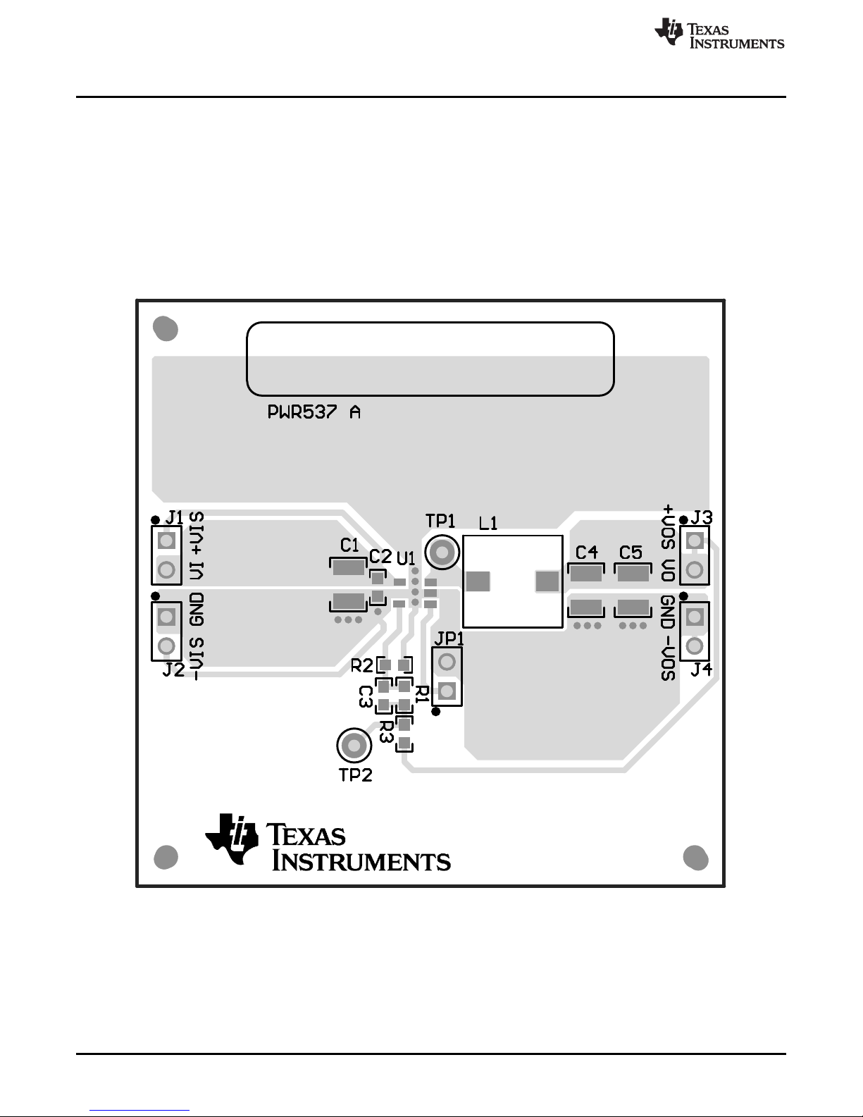
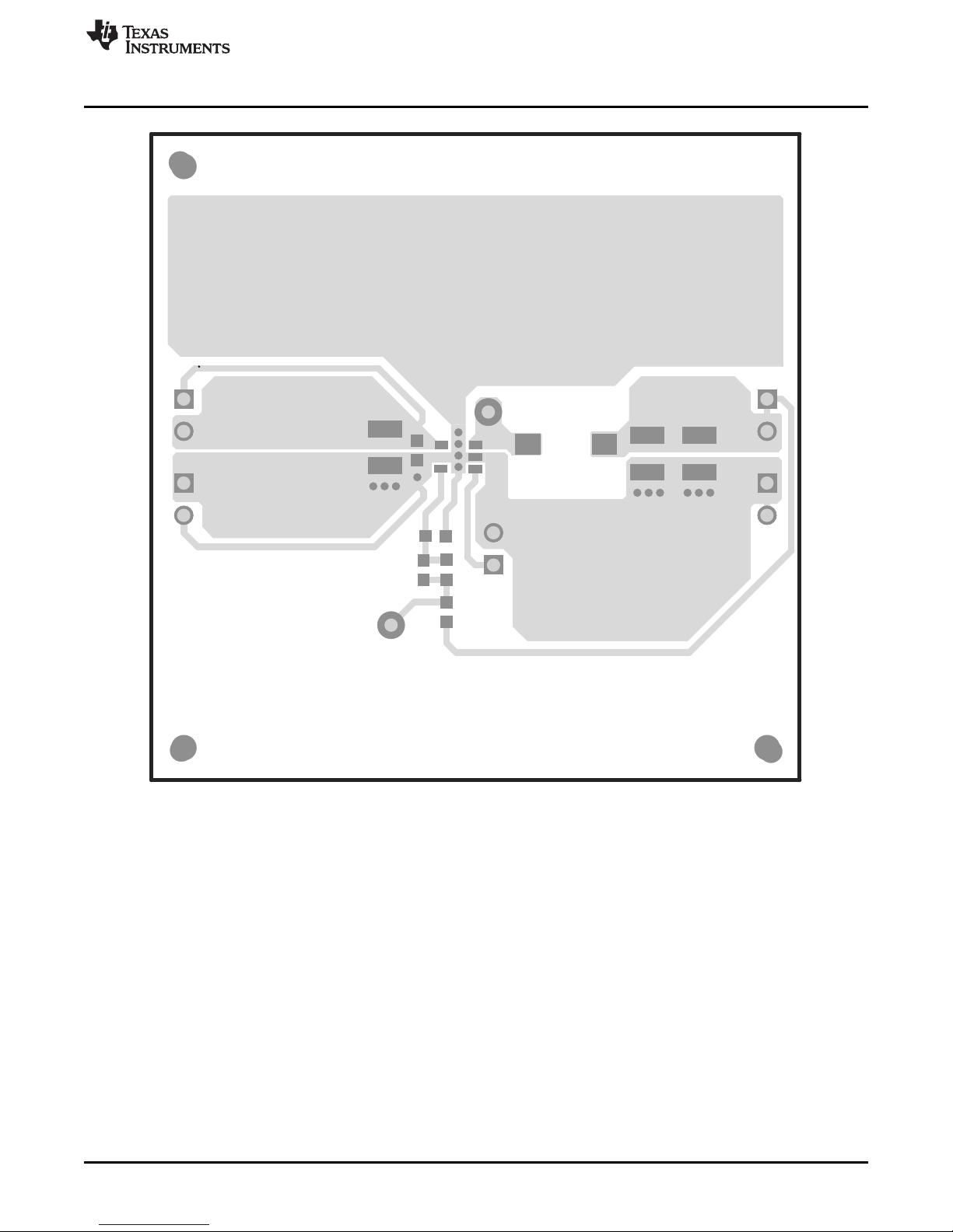
5 Board Layout
This section provides a description of the TPS560200EVM-537, board layout, and layer illustrations.
5.1 Layout
The board layout for the TPS560200EVM-537 is shown in Figure 15 through Figure 17. The top layer
contains the main power traces for VIN, VOUT, and ground. Also on the top layer are connections for the
pins of the TPS560200 and a large area filled with ground. All of the signal traces also are located on the
top side. The input decoupling capacitors, C1 and C2, are located as close to the IC as possible. The
input and output connectors, test points, and all of the components are located on the top side. The
bottom layer is a ground plane.
www.ti.com
12
TPS560200EVM-537 0.5-A, Single Channel Regulator Evaluation Module SLVU954–September 2013
Figure 15. Top Assembly
Copyright © 2013, Texas Instruments Incorporated
Submit Documentation Feedback
Page 13
www.ti.com
Board Layout
SLVU954–September 2013 TPS560200EVM-537 0.5-A, Single Channel Regulator Evaluation Module
Submit Documentation Feedback
Figure 16. Top Layer
13
Copyright © 2013, Texas Instruments Incorporated
Page 14

Board Layout
www.ti.com
14
TPS560200EVM-537 0.5-A, Single Channel Regulator Evaluation Module SLVU954–September 2013
Figure 17. Bottom Layer
Copyright © 2013, Texas Instruments Incorporated
Submit Documentation Feedback
Page 15

10µF
C4
10µHL1
SH-1
10µF
C5
VIN 4.5-17V
GNDGND
VI
VOUT 1.05V
0.1µF
C2
+VOS+VIS
-VIS -VOS
C3
TPS560200
VIN
4
EN
1
VSENSE5GND
2
PH
3
U1
1
2
J3
1
2
J4
1
2
J2
1
2
JP1
0
R3
VO
TP2
TP1
1
2
J1
10µF
C1
6.19k
R1
20.0k
R2
open
www.ti.com
6 Schematic, Bill of Materials, and Reference
6.1 Schematic
Figure 18 is the schematic for the TPS560200EVM-537.
Figure 18. TPS560200EVM-537Schematic Diagram
Schematic, Bill of Materials, and Reference
SLVU954–September 2013 TPS560200EVM-537 0.5-A, Single Channel Regulator Evaluation Module
Submit Documentation Feedback
Copyright © 2013, Texas Instruments Incorporated
15
Page 16

Schematic, Bill of Materials, and Reference
www.ti.com
6.2 Bill of Materials
Table 5. Bill of Materials
Designator Qty Value Description Package Reference PartNumber Manufacturer
PCB 1 Printed Circuit Board PWR537 Any
C1 1 10uF CAP,CERM, 10uF, 25V, +/-10%, X5R, 1210 1210 GRM32DR61E106KA12L MuRata
C2 1 0.1uF CAP, CERM, 0.1uF, 16V, +/-5%, X7R, 0603 0603 0603YC104JAT2A AVX
C3 0 CAP, CERM 0603
C4, C5 2 10uF CAP, CERM, 10uF, 10V, +/-10%, X5R, 1210 1210 C1210C106K8PACTU Kemet
J1, J2, J3, J4, 5 Header, 100mil, 2x1, Tin plated, TH Header, 2 PIN, 100mil, Tin PEC02SAAN Sullins Connector Solutions
JP1
L1 1 10uH Inductor, Shielded Drum Core, Ferrite, 10uH, WE-PD-M 744777910 Wurth Elektronik eiSos
LBL1 1 Thermal Transfer Printable Labels, 1.250" W x PCB Label 1.25"H x 0.250"W THT-13-457-10 Brady
R1 1 6.19k RES, 6.19k ohm, 1%, 0.1W, 0603 0603 CRCW06036K19FKEA Vishay-Dale
R2 1 20.0k RES, 20.0k ohm, 1%, 0.1W, 0603 0603 CRCW060320K0FKEA Vishay-Dale
R3 1 0 RES, 0 ohm, 5%, 0.1W, 0603 0603 ERJ-3GEY0R00V Panasonic
SH-1 1 1x2 Shunt, 100mil, Gold plated, Black Shunt 969102-0000-DA 3M
TP1 1 Yellow Test Point, Miniature, Yellow, TH Yellow Miniature Testpoint 5004 Keystone
TP2 1 White Test Point, Miniature, White, TH White Miniature Testpoint 5002 Keystone
U1 1 Step Down Converter, 4.5V to 17 V Input, 500 5 Pin SOT23 TPS560200DBV5 Texas Instruments
2A, 0.045 ohm, SMD
0.250" H - 10,000 per roll
mA
6.3 Reference
1. TPS560200, 4.5V to 17V Input, 0.5-A Synchronous Step-Down SWIFT™ Converter with Advanced
Eco-mode™ data sheet (SLVSC81)
16
TPS560200EVM-537 0.5-A, Single Channel Regulator Evaluation Module SLVU954–September 2013
Copyright © 2013, Texas Instruments Incorporated
Submit Documentation Feedback
Page 17

IMPORTANT NOTICE
Texas Instruments Incorporated and its subsidiaries (TI) reserve the right to make corrections, enhancements, improvements and other
changes to its semiconductor products and services per JESD46, latest issue, and to discontinue any product or service per JESD48, latest
issue. Buyers should obtain the latest relevant information before placing orders and should verify that such information is current and
complete. All semiconductor products (also referred to herein as “components”) are sold subject to TI’s terms and conditions of sale
supplied at the time of order acknowledgment.
TI warrants performance of its components to the specifications applicable at the time of sale, in accordance with the warranty in TI’s terms
and conditions of sale of semiconductor products. Testing and other quality control techniques are used to the extent TI deems necessary
to support this warranty. Except where mandated by applicable law, testing of all parameters of each component is not necessarily
performed.
TI assumes no liability for applications assistance or the design of Buyers’ products. Buyers are responsible for their products and
applications using TI components. To minimize the risks associated with Buyers’ products and applications, Buyers should provide
adequate design and operating safeguards.
TI does not warrant or represent that any license, either express or implied, is granted under any patent right, copyright, mask work right, or
other intellectual property right relating to any combination, machine, or process in which TI components or services are used. Information
published by TI regarding third-party products or services does not constitute a license to use such products or services or a warranty or
endorsement thereof. Use of such information may require a license from a third party under the patents or other intellectual property of the
third party, or a license from TI under the patents or other intellectual property of TI.
Reproduction of significant portions of TI information in TI data books or data sheets is permissible only if reproduction is without alteration
and is accompanied by all associated warranties, conditions, limitations, and notices. TI is not responsible or liable for such altered
documentation. Information of third parties may be subject to additional restrictions.
Resale of TI components or services with statements different from or beyond the parameters stated by TI for that component or service
voids all express and any implied warranties for the associated TI component or service and is an unfair and deceptive business practice.
TI is not responsible or liable for any such statements.
Buyer acknowledges and agrees that it is solely responsible for compliance with all legal, regulatory and safety-related requirements
concerning its products, and any use of TI components in its applications, notwithstanding any applications-related information or support
that may be provided by TI. Buyer represents and agrees that it has all the necessary expertise to create and implement safeguards which
anticipate dangerous consequences of failures, monitor failures and their consequences, lessen the likelihood of failures that might cause
harm and take appropriate remedial actions. Buyer will fully indemnify TI and its representatives against any damages arising out of the use
of any TI components in safety-critical applications.
In some cases, TI components may be promoted specifically to facilitate safety-related applications. With such components, TI’s goal is to
help enable customers to design and create their own end-product solutions that meet applicable functional safety standards and
requirements. Nonetheless, such components are subject to these terms.
No TI components are authorized for use in FDA Class III (or similar life-critical medical equipment) unless authorized officers of the parties
have executed a special agreement specifically governing such use.
Only those TI components which TI has specifically designated as military grade or “enhanced plastic” are designed and intended for use in
military/aerospace applications or environments. Buyer acknowledges and agrees that any military or aerospace use of TI components
which have not been so designated is solely at the Buyer's risk, and that Buyer is solely responsible for compliance with all legal and
regulatory requirements in connection with such use.
TI has specifically designated certain components as meeting ISO/TS16949 requirements, mainly for automotive use. In any case of use of
non-designated products, TI will not be responsible for any failure to meet ISO/TS16949.
Products Applications
Audio www.ti.com/audio Automotive and Transportation www.ti.com/automotive
Amplifiers amplifier.ti.com Communications and Telecom www.ti.com/communications
Data Converters dataconverter.ti.com Computers and Peripherals www.ti.com/computers
DLP® Products www.dlp.com Consumer Electronics www.ti.com/consumer-apps
DSP dsp.ti.com Energy and Lighting www.ti.com/energy
Clocks and Timers www.ti.com/clocks Industrial www.ti.com/industrial
Interface interface.ti.com Medical www.ti.com/medical
Logic logic.ti.com Security www.ti.com/security
Power Mgmt power.ti.com Space, Avionics and Defense www.ti.com/space-avionics-defense
Microcontrollers microcontroller.ti.com Video and Imaging www.ti.com/video
RFID www.ti-rfid.com
OMAP Applications Processors www.ti.com/omap TI E2E Community e2e.ti.com
Wireless Connectivity www.ti.com/wirelessconnectivity
Mailing Address: Texas Instruments, Post Office Box 655303, Dallas, Texas 75265
Copyright © 2015, Texas Instruments Incorporated
 Loading...