

TPS5511
3-CHANNEL POWER SUPPLY SUPERVISOR
SLVS170 – AUGUST 1998
D
Over Voltage Protection and Lock Out for
5 V, 3.3 V, and 12 V
D
Fault Protection Output with Open Drain
Output Stage
D
Open Drain Power Good Output Signal for
Power Good Input, 5 V and 3.3 V
D
300 ms Power Good Delay
D
2.3 ms PSON Control to FPO Turn-Off Delay
D
38 ms PSON Control Debounce
D
73 µs Width Noise Deglitches
D
Wide Power Supply Voltage Range
from 4 V to 15 V
D OR P PACKAGE
(TOP VIEW)
PGI
1
GND
FPO
PSON
2
3
4
PGO
8
V
7
CC
VS5
6
5
VS33
description
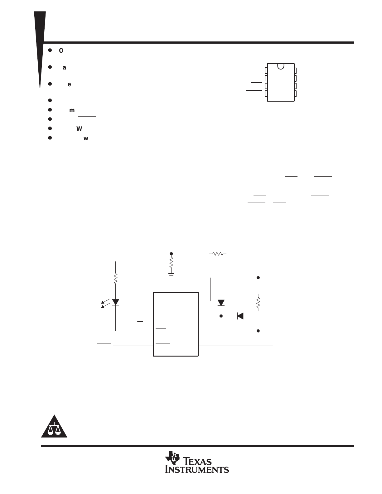
The TPS551 1 is designed to minimize the external components of personal-computer switching power supply
systems. It provides protection circuits, power good indicator, fault protection output (FPO
OVP (over voltage protection) monitors 5 V, 3.3 V , and 12 V (12 V OV detects via V
condition is detected, the PGO (power good output) is asserted low and FPO
to high resets the protection latch. There is a 2.3-ms turn-off delay from PSON
is latched high. PSON from low
to FPO. There is no delay during
turn on.
Power good feature monitors PGI, 5 V and 3.3 V under voltages and issues a power good signal when they are
ready .
), and PSON control.
terminal). When an OV
CC
The TPS5511 is characterized for operation from T
5 V
SB
TPS5511
1
PSON
2
3
4
PGI
GND
FPO
PSON
PGO
V
CC
VS5
VS33
Figure 1. TPS5511 Typical Application
= –40°C to 125°C junction temperature.
J
PGI
PGO
8
7
6
5
0.5 V
Drop
12 V
V
SB
5 V
3.3 V
Please be aware that an important notice concerning availability, standard warranty, and use in critical applications of
Texas Instruments semiconductor products and disclaimers thereto appears at the end of this data sheet.
PRODUCTION DATA information is current as of publication date.
Products conform to specifications per the terms of Texas Instruments
standard warranty. Production processing does not necessarily include
testing of all parameters.
POST OFFICE BOX 655303 • DALLAS, TEXAS 75265
Copyright 1998, Texas Instruments Incorporated
1
TPS5511
3-CHANNEL POWER SUPPLY SUPERVISOR
SLVS170 – AUGUST 1998
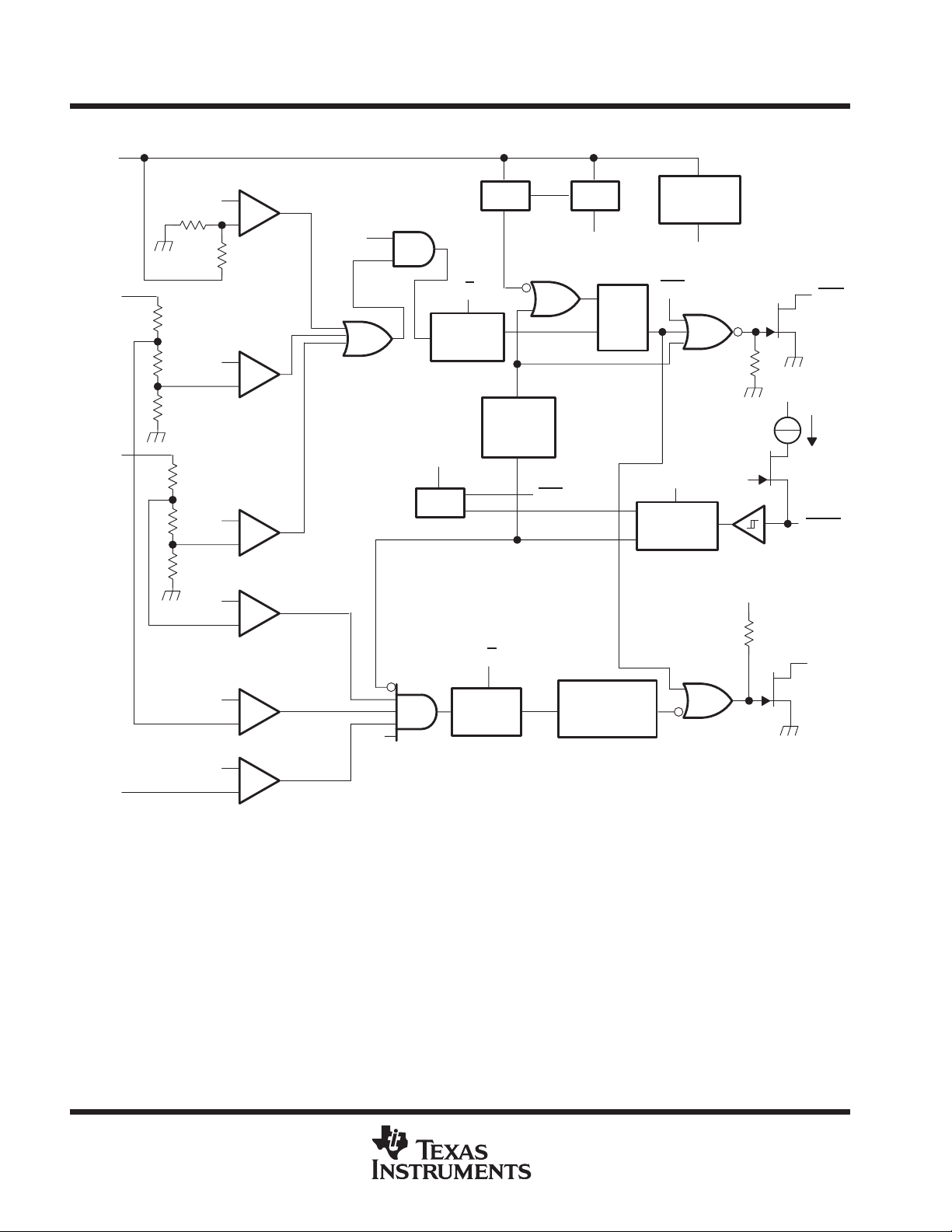
functional block diagram
V
CC
VS5
VS33
Vref
Vref
RI = 100 kΩ
Vref
RI = 100 kΩ
Vref
Vref
–
+
RI = 200 kΩ
5 OV
–
+
3.3 OV
–
+
–
3.3 UV
+
–
5 UV
+
12 OV
RST
73 µs
Debounce
Reset
OSC
Debounce
POR Vreg
Reset
R
2.3 ms
Delay
EN
R
73 µs
RTT
RST
V
CCI
R
Dominent
EN
= 3.6 V
R
S
Reset
Latch
300 ms
Delay
Counter
RTT
Q
Reset
38 ms
Debounce
Bandgap
Reference
Vref
1.192 V
V
150 µA
CCI
V
V
CC
Pull-High
Resistor
FPO
CC
PSON
PGO
RST
Vref
PGI
2
–
+
POST OFFICE BOX 655303 • DALLAS, TEXAS 75265
I/O
DESCRIPTION
Output voltage, V
Output sink current, I
3-CHANNEL POWER SUPPLY SUPERVISOR
Terminal Functions
TERMINAL
NAME NO.
VS33 5 I 3.3 V over/under voltage protection input pin
VS5 6 I 5 V over/under voltage protection input pin
GND 2 Ground
FPO 3 O Inverted fault protection output, open drain output stage
PGI 1 I Power good input signal pin
PGO 8 O Power good output signal pin, open drain output stage
PSON 4 I ON/OFF control input pin
V
CC
7 I Supply voltage/12 V over voltage protection input pin
DISSIPATION RATING TABLE
PACKAGE
P 1092 mW 8.74 mW/°C 218 mW
D 730 mW 5.84 mW/°C 146 mW
TA ≤ 25°C
POWER RATING
OPERATING FACTOR
ABOVE TA = 25°C
TPS5511
SLVS170 – AUGUST 1998
TA = 125°C
POWER RATING
absolute maximum ratings over operating free-air temperature (unless otherwise noted)
Supply voltage, V
Output voltage, V
Output voltage, V
Supply current, I
, (see Note1) 16 V. . . . . . . . . . . . . . . . . . . . . . . . . . . . . . . . . . . . . . . . . . . . . . . . . . . . . . . . . . . .
CC
(FPO) 16 V. . . . . . . . . . . . . . . . . . . . . . . . . . . . . . . . . . . . . . . . . . . . . . . . . . . . . . . . . . . . . . . . . . .
O
(PGO) 8 V. . . . . . . . . . . . . . . . . . . . . . . . . . . . . . . . . . . . . . . . . . . . . . . . . . . . . . . . . . . . . . . . . . .
O
. . . . . . . . . . . . . . . . . . . . . . . . . . . . . . . . . . . . . . . . . . . . . . . . . . . . . . . . . . . . . . . . . . . . . . . .
CC
†
1 mA
Continuous total power dissipation see Dissipation Rating Table. . . . . . . . . . . . . . . . . . . . . . . . . . . . . . . . . . . . . .
Operating junction temperature range, T
Storage temperature range, T
–65°C to 150°C. . . . . . . . . . . . . . . . . . . . . . . . . . . . . . . . . . . . . . . . . . . . . . . . . . .
stg
–40°C to 125°C. . . . . . . . . . . . . . . . . . . . . . . . . . . . . . . . . . . . . . . . . . .
J
Lead temperature, 1,6 mm (1/16 inch) from case for 10 seconds 260°C. . . . . . . . . . . . . . . . . . . . . . . . . . . . . . .
†
Stresses beyond those listed under “absolute maximum ratings” may cause permanent damage to the device. These are stress ratings only, and
functional operation of the device at these or any other conditions beyond those indicated under “recommended operating conditions” is not
implied. Exposure to absolute-maximum-rated conditions for extended periods may affect device reliability.
NOTE 1: All voltages are with respect to the device GND terminal.
recommended operating conditions
TEST CONDITIONS MIN TYP MAX UNIT
Supply voltage, V
Input voltage, V
p
Operating junction temperature, T
p
Supply voltage rising time, t
NOTE 2: VCC rising and falling slew rate must be less then 14 V/ms.
CC
I
O
J
O(sink)
r
PSON, VS5, VS33, PGI 7 V
FPO 15 V
PGO 7 V
FPO 30 mA
PGO 10 mA
4 15 V
–40 125 °C
See Note 2 1 ms
POST OFFICE BOX 655303 • DALLAS, TEXAS 75265
3

TPS5511
V
L
(FPO)
V
Under-voltage threshold
V
3-CHANNEL POWER SUPPLY SUPERVISOR
SLVS170 – AUGUST 1998
electrical characteristics, VCC = 5 V, TJ = full range. (unless otherwise specified)
over voltage protection
PARAMETER TEST CONDITIONS MIN TYP MAX UNIT
VS33 3.9 4.1 4.3
Over-voltage threshold
I
Leakage current (FPO) V(FPO) = 5 V 5 µA
LKG
ow level output voltage
OL
PGI and PGO
Input threshold voltage (PGI) 1.141 1.192 1.242 V
I
Leakage current (PGO) PGO = 5 V 5 µA
LKG
V
Low level output voltage (PGO) Sink current = 10 mA 0.4 V
OL
PARAMETER TEST CONDITIONS MIN TYP MAX UNIT
VS5 5.7 6.1 6.5
V
CC
I
= 10 mA 0.3
sink
I
= 30 mA 0.7
sink
VS33 2.71 2.83 2.95
VS5 4.1 4.3 4.47
13.3 13.8 14.3
V
PSON control
PARAMETER TEST CONDITIONS MIN TYP MAX UNIT
Input pull-up current PSON = 0 V 150 µA
High-level input voltage 2.4 V
Low-level input voltage 1.2 V
total device
PARAMETER TEST CONDITIONS MIN TYP MAX UNIT
I
Supply current PSON = 5 V 1 mA
CC
switching characteristics, VCC = 5 V, TJ = full range
PARAMETER TEST CONDITIONS MIN TYP MAX UNIT
t
Delay time (PGI to PGO) 200 300 450 ms
d1
t
De-bounce time (PSON) 24 38 57 ms
b
Noise deglitch time 47 73 110 µs
t
PSON to FPO delay time tb + 1.1 tb + 2.3 tb + 4 ms
d2
4
POST OFFICE BOX 655303 • DALLAS, TEXAS 75265
timing chart
V
CC
Reset
R
PSON
S
Q
FPO
TPS5511
3-CHANNEL POWER SUPPLY SUPERVISOR
SLVS170 – AUGUST 1998
PGI
3.3 V
5 V
12 V
PGO
t
d1
Protect Occur
t
b
t
d1
t
d2
t
b
PSON
OFF
PSON
PG Off Delay
ON
t
d1
AC
OFF
POST OFFICE BOX 655303 • DALLAS, TEXAS 75265
5

TPS5511
3-CHANNEL POWER SUPPLY SUPERVISOR
SLVS170 – AUGUST 1998
MECHANICAL DATA
D (R-PDSO-G**) PLASTIC SMALL-OUTLINE PACKAGE
14 PIN SHOWN
0.050 (1,27)
14
1
0.069 (1,75) MAX
A
0.020 (0,51)
0.014 (0,35)
0.010 (0,25)
0.004 (0,10)
DIM
8
7
PINS **
0.010 (0,25)
0.157 (4,00)
0.150 (3,81)
M
0.244 (6,20)
0.228 (5,80)
Seating Plane
0.004 (0,10)
8
14
0.008 (0,20) NOM
0°–8°
16
Gage Plane
0.010 (0,25)
0.044 (1,12)
0.016 (0,40)
A MAX
A MIN
NOTES: A. All linear dimensions are in inches (millimeters).
6
B. This drawing is subject to change without notice.
C. Body dimensions do not include mold flash or protrusion, not to exceed 0.006 (0,15).
D. Falls within JEDEC MS-012
POST OFFICE BOX 655303 • DALLAS, TEXAS 75265
0.197
(5,00)
0.189
(4,80)
0.344
(8,75)
0.337
(8,55)
0.394
(10,00)
0.386
(9,80)
4040047/D 10/96

TPS5511
3-CHANNEL POWER SUPPLY SUPERVISOR
SLVS170 – AUGUST 1998
MECHANICAL DATA
P (R-PDIP-T8) PLASTIC DUAL-IN-LINE PACKAGE
0.400 (10,60)
0.355 (9,02)
58
0.260 (6,60)
0.240 (6,10)
41
0.070 (1,78) MAX
0.020 (0,51) MIN
0.200 (5,08) MAX
0.125 (3,18) MIN
0.100 (2,54)
0.021 (0,53)
0.015 (0,38)
NOTES: A. All linear dimensions are in inches (millimeters).
B. This drawing is subject to change without notice.
C. Falls within JEDEC MS-001
0.010 (0,25)
M
0.310 (7,87)
0.290 (7,37)
Seating Plane
0°–15°
0.010 (0,25) NOM
4040082/B 03/95
POST OFFICE BOX 655303 • DALLAS, TEXAS 75265
7

IMPORTANT NOTICE
T exas Instruments and its subsidiaries (TI) reserve the right to make changes to their products or to discontinue
any product or service without notice, and advise customers to obtain the latest version of relevant information
to verify, before placing orders, that information being relied on is current and complete. All products are sold
subject to the terms and conditions of sale supplied at the time of order acknowledgement, including those
pertaining to warranty, patent infringement, and limitation of liability.
TI warrants performance of its semiconductor products to the specifications applicable at the time of sale in
accordance with TI’s standard warranty. Testing and other quality control techniques are utilized to the extent
TI deems necessary to support this warranty . Specific testing of all parameters of each device is not necessarily
performed, except those mandated by government requirements.
CERT AIN APPLICATIONS USING SEMICONDUCTOR PRODUCTS MAY INVOLVE POTENTIAL RISKS OF
DEATH, PERSONAL INJURY, OR SEVERE PROPERTY OR ENVIRONMENTAL DAMAGE (“CRITICAL
APPLICATIONS”). TI SEMICONDUCTOR PRODUCTS ARE NOT DESIGNED, AUTHORIZED, OR
WARRANTED TO BE SUITABLE FOR USE IN LIFE-SUPPORT DEVICES OR SYSTEMS OR OTHER
CRITICAL APPLICA TIONS. INCLUSION OF TI PRODUCTS IN SUCH APPLICATIONS IS UNDERST OOD TO
BE FULLY AT THE CUSTOMER’S RISK.
In order to minimize risks associated with the customer’s applications, adequate design and operating
safeguards must be provided by the customer to minimize inherent or procedural hazards.
TI assumes no liability for applications assistance or customer product design. TI does not warrant or represent
that any license, either express or implied, is granted under any patent right, copyright, mask work right, or other
intellectual property right of TI covering or relating to any combination, machine, or process in which such
semiconductor products or services might be or are used. TI’s publication of information regarding any third
party’s products or services does not constitute TI’s approval, warranty or endorsement thereof.
Copyright 1998, Texas Instruments Incorporated
 Loading...