

Page 1

User's Guide
SLUUBN2–March 2017
TPS549B22EVM-847, 25-A Single Synchronous Step-Down
Converter With Full Differential Sense and PMBus™
This user's guide describes the characteristics, operation, and use of the TPS549B22 Evaluation Module
(EVM). The user's guide includes test information, descriptions, and results. A complete schematic
diagram, printed-circuit board layouts, and bill of materials are also included in this document. Throughout
this user's guide, the abbreviations EVM, TPS549B22EVM, and the term evaluation module are
synonymous with the TPS549B22EVM-847, unless otherwise noted.
Contents
1 Introduction ................................................................................................................... 3
1.1 Before You Begin ................................................................................................... 3
2 Description.................................................................................................................... 4
2.1 Typical End-User Applications .................................................................................... 4
2.2 EVM Features....................................................................................................... 4
3 EVM Electrical Performance Specifications .............................................................................. 5
4 Schematic..................................................................................................................... 6
5 Test Setup .................................................................................................................... 7
5.1 Test and Configuration Software ................................................................................. 7
6 Test Equipment .............................................................................................................. 8
7 PWR-847EVM................................................................................................................ 9
8 List of Test Points, Jumpers, and Switch ............................................................................... 11
9 EVM Configuration Using the Fusion GUI .............................................................................. 12
10 Test Procedure ............................................................................................................. 13
10.1 Line and Load Regulation Measurement Procedure ......................................................... 13
10.2 Efficiency ........................................................................................................... 13
10.3 Equipment Shutdown ............................................................................................. 13
11 Performance Data and Typical Characteristic Curves................................................................. 14
11.1 Efficiency ........................................................................................................... 14
11.2 Load Regulation ................................................................................................... 14
11.3 Line Regulation.................................................................................................... 15
11.4 Transient Response............................................................................................... 18
11.5 Output Ripple ...................................................................................................... 18
11.6 Control On.......................................................................................................... 19
11.7 Control Off.......................................................................................................... 20
11.8 Thermal Image..................................................................................................... 21
12 Fusion GUI ................................................................................................................. 22
13 EVM Assembly Drawing and PCB Layout .............................................................................. 33
14 List of Materials............................................................................................................. 38
1 PWR-847EVM Schematic .................................................................................................. 6
2 PWR-847EVM Overview.................................................................................................... 9
3 Tip and Barrel Measurement............................................................................................... 9
4 EVM and USB Interface Adapter......................................................................................... 10
5 Efficiency vs Output Current SKIP Mode ............................................................................... 14
6 Power Loss vs Output Current SKIP Mode............................................................................. 14
SLUUBN2–March 2017
Submit Documentation Feedback
List of Figures
TPS549B22EVM-847, 25-A Single Synchronous Step-Down Converter With
Copyright © 2017, Texas Instruments Incorporated
Full Differential Sense and PMBus™
1
Page 2

www.ti.com
7 Line Regulation of 1-V Output............................................................................................ 15
8 PMBus V
9 PMBus V
10 PMBus V
11 PMBus V
Step-Up = 0.6 V to 1.2 V at 0 A........................................................................... 15
OUT
Step-Down = 1.2 V to 0.6 V at 0 A ....................................................................... 16
OUT
Step-Up = 0.6 V to 1.2 V at 25 A ......................................................................... 16
OUT
Step-Down = 1.2 V to 0.6 V at 25 A...................................................................... 17
OUT
12 PMBUS Multiple Commands ............................................................................................. 17
13 Transient Response of 1-V Output at 12 V
14 Output Ripple and SW Node of 1-V Output at 12 V
15 Output Ripple and SW Node of 1-V Output at 12 V
16 Start up from Control, 1-V Output at 12 V
17 0.5-V Pre-bias start up from Control, 1-V Output at 12 V
18 Start-Up and Shutdown, 1-V Output at 12 V
19 Thermal Image at 1-V Output at 12 V
, Transient is 0.5 A to 15.5 A, the Step is 15 A at 40 A/µs....... 18
IN
, 25-A Output ................................................. 18
IN
, 0-A Output .................................................. 19
IN
, 0-A Output .............................................................. 19
IN
, 10-A Output ........................................... 20
IN
, 0.5-A Output......................................................... 20
IN
, 25-A Output, 650 kHz at 25°C Ambient ................................. 21
IN
20 First Window at Fusion Launch .......................................................................................... 22
21 Scan Finds Device Successfully ......................................................................................... 22
22 Software Launch Continued .............................................................................................. 22
23 Software Launch Continued .............................................................................................. 22
24 First Screen After Successful Launch Configure: Limits and On/Off................................................ 23
25 Configure: Frequency- FS Configuration Pop-up ...................................................................... 24
26 Configure: Frequency- FS Config Pop-Up with Change .............................................................. 25
27 Configure: Store Config to NVM.......................................................................................... 26
28 Change View Screen to Monitor Screen................................................................................ 27
29 System Dashboard......................................................................................................... 28
30 Status Screen............................................................................................................... 29
31 Store Configuration To Memory.......................................................................................... 30
32 PMBus Logging............................................................................................................. 31
33 PMBus Log Details......................................................................................................... 32
34 PWR-847EVM Top Layer Assembly Drawing (Top View)............................................................ 33
35 PWR-847EVM Top Solder Mask (Top View)........................................................................... 33
36 PWR-847EVM Top Layer (Top View) ................................................................................... 34
37 PWR-847EVM Inner Layer 1 (Top View) ............................................................................... 34
38 PWR-847EVM Inner Layer 2 (Top View) ............................................................................... 35
39 PWR-847EVM Inner Layer 3 (Top View) ............................................................................... 35
40 PWR-847EVM Inner Layer 4 (Top View) ............................................................................... 36
41 PWR-847EVM Bottom Layer (Top View) ............................................................................... 36
42 PWR-847EVM Bottom Solder Mask (Top View)....................................................................... 37
43 PWR-847EVM Bottom Overlay Layer (Top View) ..................................................................... 37
1 PWR-847EVM Electrical Performance Specifications .................................................................. 5
2 Test Point Functions ....................................................................................................... 11
3 Key Factory Configuration Parameters.................................................................................. 12
4 List of Test Points for Line and Load Measurements ................................................................. 13
5 List of Test Points for Efficiency Measurements ....................................................................... 13
6 PWR847 List of Materials ................................................................................................. 38
2
TPS549B22EVM-847, 25-A Single Synchronous Step-Down Converter With
Full Differential Sense and PMBus™
List of Tables
Copyright © 2017, Texas Instruments Incorporated
Submit Documentation Feedback
SLUUBN2–March 2017
Page 3
!
www.ti.com
1 Introduction
The PWR847EVM evaluation module uses the TPS549B22 device. The TPS549B22 is a highly integrated
synchronous buck converter that is designed for up to 25-A current output.
1.1 Before You Begin
The following warnings and cautions are noted for the safety of anyone using or working close to the
TPS549B22EVM-847. Observe all safety precautions.
The circuit module has signal traces, components, and component
leads on the bottom of the board. This may result in exposed
voltages, hot surfaces or sharp edges. Do not reach under the
board during operation.
Introduction
Warning The TPS549B22EVM-847 circuit module may become hot
during operation due to dissipation of heat. Avoid contact with
the board. Follow all applicable safety procedures applicable
to your laboratory.
Caution Do not leave the EVM powered when unattended.
WARNING
CAUTION
The circuit module may be damaged by over temperature. To avoid damage,
monitor the temperature during evaluation and provide cooling, as needed, for
your system environment.
CAUTION
Some power supplies can be damaged by application of external voltages. If
using more than 1 power supply, check your equipment requirements and use
blocking diodes or other isolation techniques, as needed, to prevent damage to
your equipment.
CAUTION
The communication interface is not isolated on the EVM. Be sure no ground
potential exists between the computer and the EVM. Also be aware that the
computer is referenced to the Battery- potential of the EVM.
SLUUBN2–March 2017
Submit Documentation Feedback
TPS549B22EVM-847, 25-A Single Synchronous Step-Down Converter With
Copyright © 2017, Texas Instruments Incorporated
Full Differential Sense and PMBus™
3
Page 4

Description
2 Description
The PWR-847EVM is designed as a single output DC-DC converter that demonstrates the TPS549B22 in
a typical low-voltage application while providing a number of test points to evaluate the performance. It
uses a nominal 12-V input bus to produce a regulated 1-V output at up to 25-A load current.
2.1 Typical End-User Applications
• Enterprise Storage, SSD, NAS
• Wireless and Wired Communication Infrastructure
• Industrial PCs, Automation, ATE, PLC, Video Surveillance
• Enterprise Server, Switches, Routers
• ASIC, SoC, FPGA, DSP Core and I/O Rails
2.2 EVM Features
• Regulated 1-V output up to 25-A, steady-state output current
• Convenient test points for probing critical waveforms
• PMBus™ connector for easy connection with the TI USB adapter
www.ti.com
4
TPS549B22EVM-847, 25-A Single Synchronous Step-Down Converter With
Full Differential Sense and PMBus™
Copyright © 2017, Texas Instruments Incorporated
Submit Documentation Feedback
SLUUBN2–March 2017
Page 5
www.ti.com
3 EVM Electrical Performance Specifications
Table 1 lists the PWR-847EVM electrical performance specifications.
Table 1. PWR-847EVM Electrical Performance Specifications
Parameter Test Conditions Min Typ Max Units
Input Characteristics
Voltage range VINtied to VDD 5 12 14 V
Maximum input current VIN= 12 V, IO= 25 A 12 A
No load input current VIN= 12 V, IO= 0 A 60 mA
Output Characteristics
V
Output voltage Output current = 10 A 1 V
OUT
I
Output load current I
OUT
Output voltage regulation
V
Output voltage ripple VIN= 12 V, I
OUT
V
Output overcurrent 32 A
OUT
Systems Characteristics
Switching frequency F
V
Peak efficiency VIN= 12 V, IO= 12 A, FSW= 650 kHz 90%
OUT
Operating temperature T
to I
OUT(min)
OUT(max)
Line regulation: input voltage = 5 V to 14 V 0.5%
Load regulation: output current = 0 A to I
= 25 A 10 mV
OUT
SW
oper
EVM Electrical Performance Specifications
0 25 A
OUT(max)
0.5%
650 kHz
0 85 ºC
PP
SLUUBN2–March 2017
Submit Documentation Feedback
TPS549B22EVM-847, 25-A Single Synchronous Step-Down Converter With
Copyright © 2017, Texas Instruments Incorporated
Full Differential Sense and PMBus™
5
Page 6
PGND
22uF
C16
DNP
22uF
C15
DNP
22uF
C14
DNP
22µF
C13
330uF
C12
DNP
330uFC1DNP
2200pF
C10
22µF
C2
22µF
C9
22µF
C8
22µF
C7
22µF
C6
22µF
C5
22µF
C4
22µF
C3
DRGND
1uF
C34
DNP
1µF
C35
100µF
C33
100µF
C40
100µF
C41
DNP
100µF
C42
100µF
C29
0.1µF
C22
330nH
L1
TP3
CHB
100µF
C27
DNP
100µF
C28
DNP
100µF
C39
6800pF
C32
DNP
TP7
CHA
470pF
C21
DNP
0.1uF
C31
DNP
100µF
C26
100µF
C25
0
R14
DNP1000pF
C36
DNP
3.01
R9
DNP
1uF
C44DNP
4.7µF
C45
TP12
ILIM
0
R4
AGND
DRGND
DRGND
470uF
C37
DNP
470µF
C24
470µF
C38
470µF
C23
DNP
0
R16
1000pF
C46DNP
AGND
0
R2
DNP
0
R3
DNP
TP8
PGOOD
100k
R13
PGND
TP13
AGND PGND DRGND
CNTL
CLK
DATA
ALERT
MODE
FSEL
VSEL
PGND
PGND
PGND
100µF
C11
TP2
TP10
1 2
3 4
5 6
7 8
9 10
J6
DATA
CLK
ALERT
PMBus
AGND
----- GND NET TIES -----
Remote Sense pos/neg should run as balanced pair
VIN = 6V - 16V
I_OUT = 25A MAX
22uF
C17
DNP
22uF
C18
DNP
22uF
C19
DNP
22µF
C20
DNP
TP6
TP11
0
R17
DNP
0
R18
DNP
1.00
R1
0
R10
1.10k
R8
1.50k
R5
DNP
NT1
Net-Tie
NT2
Net-Tie
TP5
SW
TP4
MODE FSELVSEL
25.5k
R25
AGND
CNTL/EN_UVLO
LOW
10.0k
R15
TP9
BP
TP14
100k
R20
100k
R21
100k
R22
BP
100uF
C43
DNP
100uF
C30
DNP
J1
200k
R6
100k
R12
J4
TP1
VDD
TP17
FSEL
TP16
MODE
TP15
VSEL
0
R11
VDD
TP18
PGND
TP19
TP20
CLK
TP21
DATA
TP22
ALERT
61.9k
R19
37.4k
R23
42.2k
R24
0
R7
J2
J3
J5
VOUT = 1V
NetC31_1
NetC31_1
DRGND
BP
SMB_ALRT#
1
PMB_DATA
2
PMB_CLK
3
EN_UVLO
4
BOOT
5
NC
6
NC
7
SW
8
SW
9
SW
10
SW
11
SW
12
PGND
13
PGND
14
PGND
15
PGND
16
PGND
17
PGND
18
PGND
19
PGND
20
PVIN
21
PVIN
22
PVIN
23
PVIN
24
PVIN
25
NC
26
NC
27
VDD
28
DRGND
29
AGND
30
BP
31
ADDR
32
VSEL
33
MODE
34
PGOOD
35
ILIM
36
RESV_TRK
37
RSN
38
RSP
39
VOSNS
40
PAD
41
U1
TPS549B22RVFR
Copyright © 2017, Texas Instruments Incorporated
Schematic
www.ti.com
6
SLUUBN2– March 2017
Submit Documentation Feedback
Copyright © 2017, Texas Instruments Incorporated
TPS549B22EVM-847, 25-A Single Synchronous Step-Down Converter With Full
Differential Sense and PMBus™
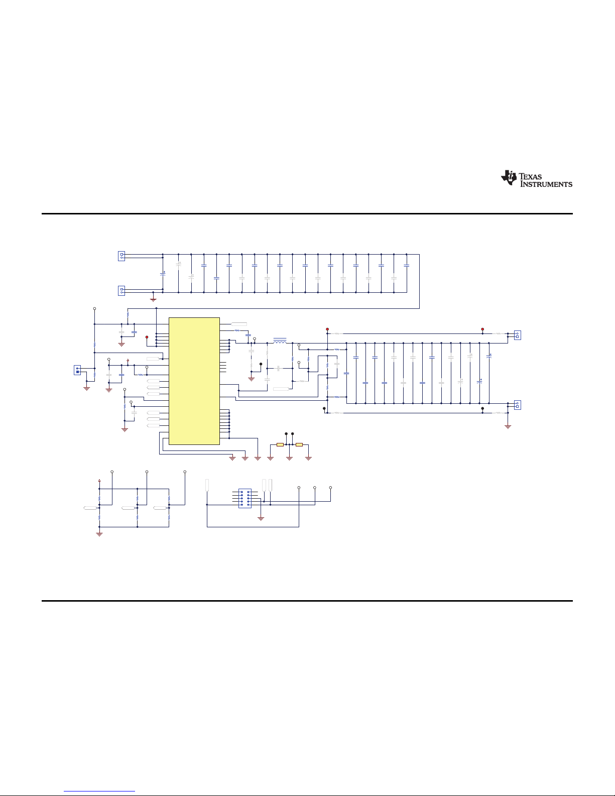
4 Schematic
Figure 1 illustrates the PWR-847EVM schematic.
Figure 1. PWR-847EVM Schematic
Page 7

www.ti.com
5 Test Setup
5.1 Test and Configuration Software
To change any of the default configuration parameters on the EVM, it is necessary to obtain the TI Fusion
Digital Power Designer software. This can be downloaded from the TI website.
5.1.1 Description
The Fusion Digital Power Designer is the graphical user interface (GUI) used to configure and monitor the
Texas Instruments TPS549B22 power converter installed on this evaluation module. The application uses
the PMBus protocol to communicate with the controller over serial bus by way of a TI USB adapter. This
adapter can be purchased at http://www.ti.com/tool/usb-to-gpio.
NOTE: The TI USB adapter must be purchased separately. It is not included with this EVM kit.
5.1.2 Features
Some of the tasks performed with the GUI include:
• Turn on or off the power supply output, either through the hardware control line or the PMBus
operation command.
• Monitor status registers. Items such as input voltage, output voltage, output current, temperature, and
warnings and faults are continuously monitored and displayed by the GUI.
• Configure common operating characteristics such as VOUT, UVLO, soft-start time, warning and fault
thresholds, fault response, and ON/OFF.
This software is available for download at http://www.ti.com/tool/fusion_digital_power_designer.
Test Setup
SLUUBN2–March 2017
Submit Documentation Feedback
TPS549B22EVM-847, 25-A Single Synchronous Step-Down Converter With
Copyright © 2017, Texas Instruments Incorporated
Full Differential Sense and PMBus™
7
Page 8

Test Equipment
6 Test Equipment
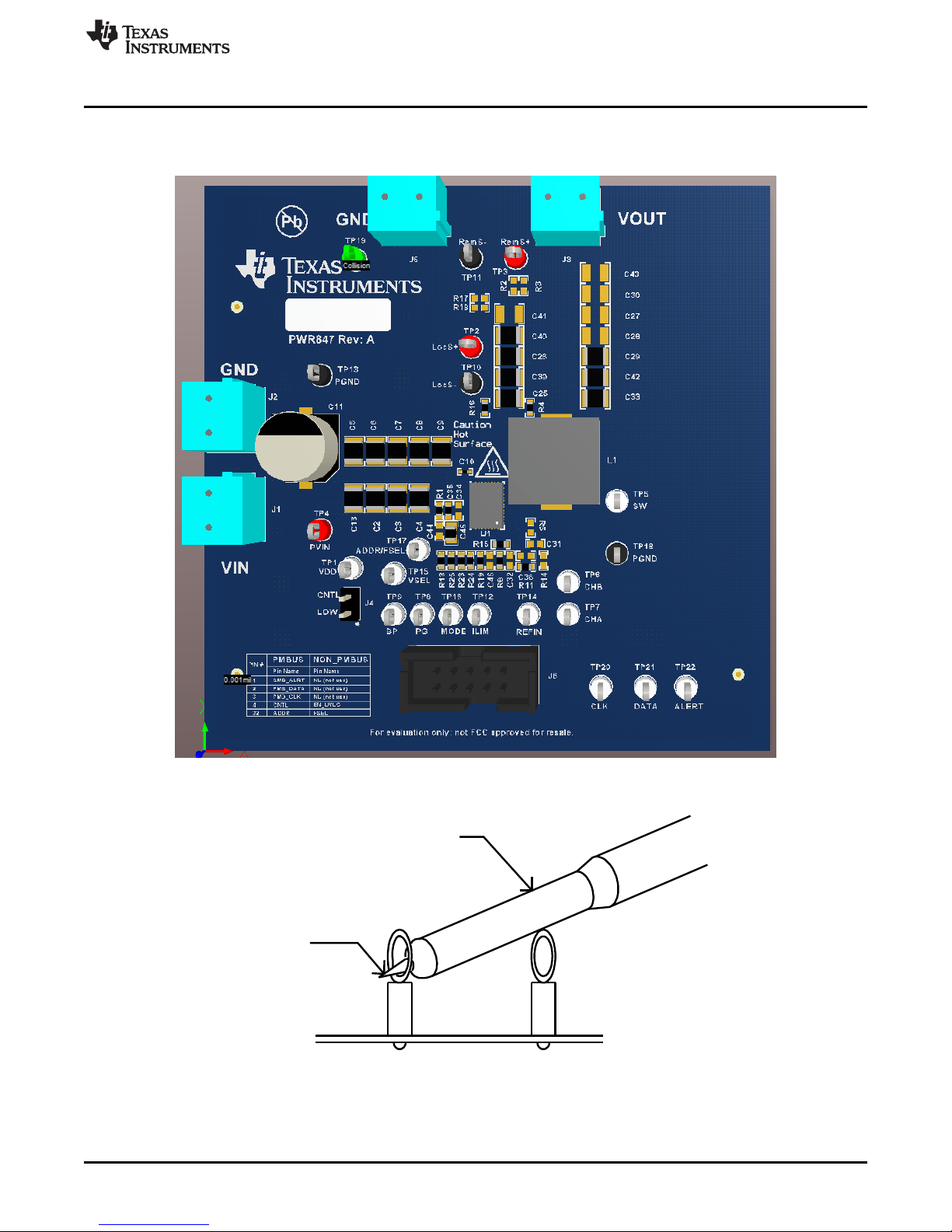
Voltage Source: The input voltage source VIN must be a 0-V to 18-V variable DC source capable of
supplying at least 12 ADC.
Multimeters: It is recommended to use two separate multimeters Figure 2. One meter is used to measure
VINand one to measure V
Output Load: A variable electronic load is recommended for testing Figure 2. It must be capable of 25 A
at voltages as low as 0.6 V.
Oscilloscope: An oscilloscope is recommended for measuring output noise and ripple. Output ripple must
be measured using a tip-and-barrel method or better as shown in Figure 3.The scope must be adjusted to
20-MHz bandwidth, AC coupling at 50 mV/division, and must be set to 1-µs/division.
Fan: During prolonged operation at high loads, it may be necessary to provide forced air cooling with a
small fan aimed at the EVM. Temperature of the devices on the EVM must be maintained below 105°C.
USB-to-GPIO Interface Adapter: A communications adapter is required between the EVM and the host
computer. This EVM was designed to use TI's USB-to-GPIO adapter. Purchase this adapter at
http://www.ti.com/tool/usb-to-gpio.
Recommended Wire Gauge: The voltage drop in the load wires must be kept as low as possible in order
to keep the working voltage at the load within its operating range. Use the AWG 14 wire (2 wires parallel
for VOUT positive and 2 wires parallel for the VOUT negative) of no more than 1.98 feet between the EVM
and the load. This recommended wire gauge and length should achieve a voltage drop of no more than
0.2 V at the maximum 25-A load.
OUT
www.ti.com
.
8
TPS549B22EVM-847, 25-A Single Synchronous Step-Down Converter With
Full Differential Sense and PMBus™
Copyright © 2017, Texas Instruments Incorporated
Submit Documentation Feedback
SLUUBN2–March 2017
Page 9
Metal Ground
Barrel
Tip
www.ti.com
7 PWR-847EVM
Figure 2 and Figure 3 illustrate the PWR-847EVM overview, tip and barrel measurement.
PWR-847EVM
SLUUBN2–March 2017
Submit Documentation Feedback
Figure 2. PWR-847EVM Overview
Figure 3. Tip and Barrel Measurement
TPS549B22EVM-847, 25-A Single Synchronous Step-Down Converter With
Copyright © 2017, Texas Instruments Incorporated
Full Differential Sense and PMBus™
9
Page 10
PWR-847EVM
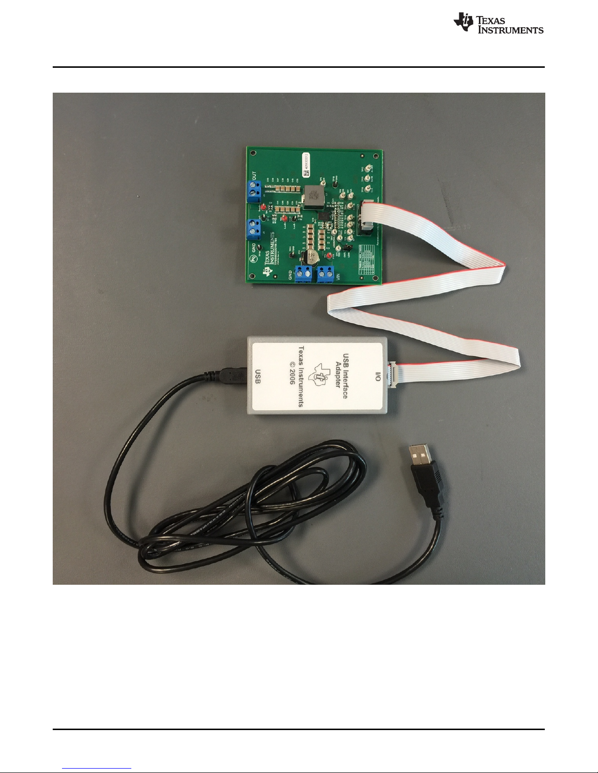
Figure 4 illustrates the EVM and USB interface adapter.
www.ti.com
10
TPS549B22EVM-847, 25-A Single Synchronous Step-Down Converter With
Full Differential Sense and PMBus™
Figure 4. EVM and USB Interface Adapter
Copyright © 2017, Texas Instruments Incorporated
Submit Documentation Feedback
SLUUBN2–March 2017
Page 11

www.ti.com
8 List of Test Points, Jumpers, and Switch
Table 2 lists the test points and their descriptions.
Table 2. Test Point Functions
Item Type Name Description
TP5 T-H loop SW Power supply Switch node
TP7 T-H loop CH-A Measure loop stability
TP6 T-H loop CH-B Measure loop stability
TP2 T-H loop LocS+
TP10 T-H loop LocS-
TP3 T-H loop RemS+ Remote sense +
TP11 T-H loop RemS- Remote sense –
TP4 T-H loop PVIN Sense VIN + across C10
TP13 T-H loop PGND Sense VIN – across C10
TP1 T-H loop VDD Supplies the internal circuitry
TP17 T-H loop ADDR Monitor the ADDR external resistor divider ratio during initial power up.
TP15 T-H loop VSEL Monitor the VSEL external resistor divider ratio during initial power up.
TP9 T-H loop BP LDO output
TP8 T-H loop PG Power good
TP16 T-H loop MODE Monitor the MODE external resistor divider ratio during initial power up.
TP12 T-H loop ILIM Program over-current limit.
TP14 T-H loop RESV_TRK Do not connect.
TP19 T-H loop PGND Common GND
TP18 T-H loop PGND Common GND
TP20 T-H loop PMB_CLK Clock input for the PMBus interface.
TP21 T-H loop PMB_DATA Data I/O for the PMBus interface.
TP22 T-H loop SMB_ALRT# Alert output for the PMBus interface.
JP4 2-pin jumper CNTL Shunts control pin to GND
Sense VOUT + locally across C25. Use for efficiency and ripple
measurements
Sense VOUT– locally across C25. Use for efficiency and ripple
measurements
List of Test Points, Jumpers, and Switch
SLUUBN2–March 2017
Submit Documentation Feedback
TPS549B22EVM-847, 25-A Single Synchronous Step-Down Converter With
Copyright © 2017, Texas Instruments Incorporated
Full Differential Sense and PMBus™
11
Page 12

EVM Configuration Using the Fusion GUI
9 EVM Configuration Using the Fusion GUI
The TPS549B22 installed on this EVM leave the factory pre-configured. See Table 3 for a short list of key
factory configuration parameters as obtained from the configuration file.
Table 3. Key Factory Configuration Parameters
www.ti.com
Cmd ID With Phase Cmd Code Hex Encoded Hex
[HiByte|LoByte]
CAPABILITY 0x19 0xD0 Max Bus: 1000 kHz; PEC: Yes; SMBALERT#: Yes
MFR_00 0xD0 0x00 0
MFR_01 (PGOOD_DLY) 0xD1 0x12 PGD:1024?s [010b], POD:1024?s [010b]
MFR_02 0xD2 0x13 CM: True, HICLOFF: True, SST: 0x00, FORCESKIPSS:
MFR_03 0xD3 0x93 FS:650 kHz [011b], RCSP:R ? 1 [01b], DCAP3:True
MFR_04 0xD4 0x80 DCAP3_Offset:0mV [00b], DCAP3_Offset_Sel:True
MFR_06 0xD6 0x05 VDDUVLO:4.25V [101b]
MFR_07 0xD7 0x8F VTRKIN:1.25V [1111b], TRKOPTION:False,
MFR_33 0xF1 0x00 0
MFR_42 0xFA 0x00 0
MFR_44 0xFC 0x0201 ID: 0x020 (TPS549B22), Revision: 0x8
ON_OFF_CONFIG 0x02 0x17 Mode: CONTROL Pin Only; Control: Active High, Turn off
OPERATION 0x01 0x00 Operation is not used to enable regulatio; Unit:
STATUS_BYTE 0x78 0x00 Status: Output Off, Vout OV Fault, IOUT OC Fault, Vin
STATUS_CML 0x7E 0x00 Status: Invalid Command, Invalid Data, PEC Fault, Other
STATUS_IOUT 0x7B 0x00 Status: Iout OC Fault, Iout OC Fault with LV Shutdown,
STATUS_VOUT 0x7A 0x00 Status: Vout OV Fault, OV Warning, UV Fault, UV
VOUT_COMMAND 0x21 0x01CD VOUT_COMMAND=0.900 V
VOUT_MARGIN_HIGH 0x25 0x0266 VOUT_MARGIN_HIGH=1.199 V
VOUT_MARGIN_LOW 0x26 0x0266 VOUT_MARGIN_LOW=1.199 V
WRITE_PROTECT 0x10 0x00 Enable Writes To All Commands
Comments
True, SEQ: False, TRK: False
SPARE:False, VPBAD:True
Immediately
ImmediateOff; Margin: None
UV Fault, Temperature, CML
Comms Fault
Iout UC Fault
Warning
If it is desired to configure the EVM to settings other than the factory settings shown in Table 3, the TI
Fusion Digital Power Designer software can be used for reconfiguration. It is necessary to have input
voltage applied to the EVM prior to launching the software so that the TPS549B22 installed is active and
able to respond to the GUI and the GUI can recognize the device.
12
TPS549B22EVM-847, 25-A Single Synchronous Step-Down Converter With
Full Differential Sense and PMBus™
Copyright © 2017, Texas Instruments Incorporated
Submit Documentation Feedback
SLUUBN2–March 2017
Page 13
www.ti.com
10 Test Procedure
10.1 Line and Load Regulation Measurement Procedure
Use the following procedures for line and load regulation measurement.
1. Connect VOUT to J3 and VOUT_GND to J5 Figure 2.
2. Ensure that the electronic load is set to draw 0 ADC.
3. Connect VIN to J1 and VIN_GND to J2 Figure 2.
4. Connect the USB interface adapter as shown in Figure 4.
5. Increase VINfrom 0 V to 12 V using the digital multimeter to measure input voltage.
6. Launch the Fusion GUI software. See the screen shots in Section 12 for more information.
7. Configure the EVM operating parameters as desired.
8. Use the other digital multimeter or the oscilloscope to measure output voltage V
as you vary the external voltage source.
Table 4. List of Test Points for Line and Load Measurements
Test Point Node Name Description
TP2 LocS+ Sense VOUT + locally across C5. Use for efficiency and ripple measurements
TP10 LocS– Sense VOUT - locally across C5. Use for efficiency and ripple measurements
TP4 PVIN Sense VIN + across C10
TP13 PGND Sense VIN - across C10
Test Procedure
at TP2 and TP10
OUT
9. Vary the load from 0 ADCto maximum rated output 25 ADC. V
Table 1.
10. Vary VINfrom 5 V to 14 V. V
11. Decrease the load to 0 A.
12. Decrease VINto 0 V or turn off the supply.
10.2 Efficiency
To measure the efficiency of the power train on the EVM, it is important to measure the voltages at the
correct location. This is necessary because otherwise the measurements will include losses in efficiency
that are not related to the power train itself. Losses incurred by the voltage drop in the copper traces and
in the input and output connectors are not related to the efficiency of the power train, and they must not be
included in efficiency measurements.
Test Point Node Name Description
TP2 LocS+ Sense VOUT + locally across C25. Use for efficiency and ripple measurements
TP10 LocS- Sense VOUT - locally across C25. Use for efficiency and ripple measurements
TP4 PVIN Sense VIN + across C10
TP13 PGND Sense VIN - across C10
Input current can be measured at any point in the input wires, and output current can be measured
anywhere in the output wires of the output being measured. Using these measurement points result in
efficiency measurements that do not include losses due to the connectors and PCB traces.
must remain in regulation as defined in
OUT
must remain in regulation as defined in Table 1.
OUT
Table 5. List of Test Points for Efficiency Measurements
10.3 Equipment Shutdown
1. Reduce the load current to 0 A.
2. Reduce input voltage to 0 V.
3. Shut down the external fan if in use.
4. Shut down equipment.
SLUUBN2–March 2017
Submit Documentation Feedback
TPS549B22EVM-847, 25-A Single Synchronous Step-Down Converter With
Copyright © 2017, Texas Instruments Incorporated
Full Differential Sense and PMBus™
13
Page 14
Load Current (A)
Converter Power Loss (W)
0 5 10 15 20 25
0
0.5
1
1.5
2
2.5
3
3.5
4
4.5
D002
VIN = 5 V
VIN = 12 V
VIN = 14 V
VIN = 18 V
Load Current (A)
Efficiency (%)
0 5 10 15 20 25
60
65
70
75
80
85
90
95
100
D001
VIN = 5 V
VIN = 12 V
VIN = 14 V
VIN = 18 V
Performance Data and Typical Characteristic Curves
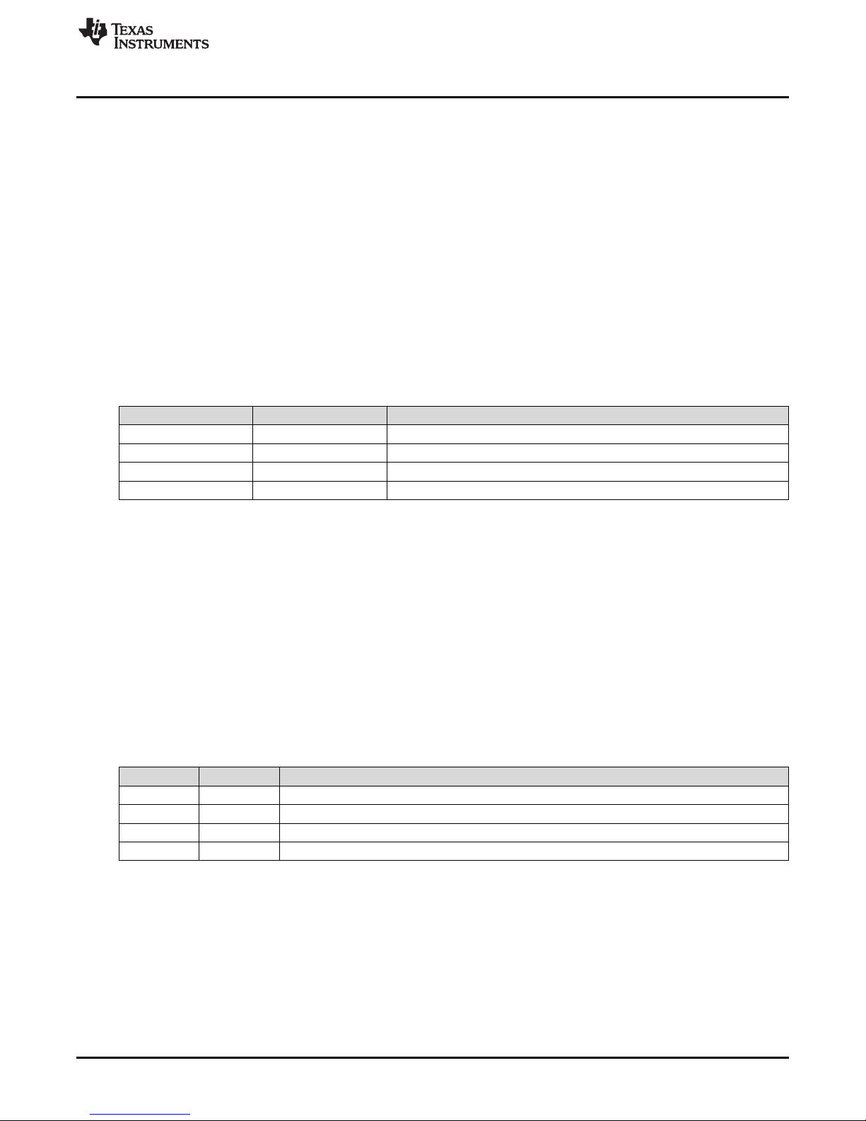
11 Performance Data and Typical Characteristic Curves
Figure 5 through Figure 18 present typical performance curves for the PWR-847EVM.
SPACE
11.1 Efficiency
www.ti.com
Figure 5. Efficiency vs Output Current SKIP Mode
11.2 Load Regulation
14
TPS549B22EVM-847, 25-A Single Synchronous Step-Down Converter With
Full Differential Sense and PMBus™
Figure 6. Power Loss vs Output Current SKIP Mode
Copyright © 2017, Texas Instruments Incorporated
Submit Documentation Feedback
SLUUBN2–March 2017
Page 15

Load Current (A)
Output Voltage Regulation (V)
0 5 10 15 20 25
0.99
0.995
1
1.005
1.01
D003
VIN = 5 V
VIN = 12 V
VIN = 14 V
VIN = 18 V
www.ti.com
11.3 Line Regulation
Performance Data and Typical Characteristic Curves
Figure 7. Line Regulation of 1-V Output
Figure 8. PMBus V
SLUUBN2–March 2017
Submit Documentation Feedback
Step-Up = 0.6 V to 1.2 V at 0 A
OUT
TPS549B22EVM-847, 25-A Single Synchronous Step-Down Converter With
Copyright © 2017, Texas Instruments Incorporated
Full Differential Sense and PMBus™
15
Page 16

Performance Data and Typical Characteristic Curves
www.ti.com
Figure 9. PMBus V
Step-Down = 1.2 V to 0.6 V at 0 A
OUT
Figure 10. PMBus V
16
TPS549B22EVM-847, 25-A Single Synchronous Step-Down Converter With
Full Differential Sense and PMBus™
Step-Up = 0.6 V to 1.2 V at 25 A
OUT
Copyright © 2017, Texas Instruments Incorporated
Submit Documentation Feedback
SLUUBN2–March 2017
Page 17

www.ti.com
Performance Data and Typical Characteristic Curves
Figure 11. PMBus V
Figure 12. PMBUS Multiple Commands
Step-Down = 1.2 V to 0.6 V at 25 A
OUT
SLUUBN2–March 2017
Submit Documentation Feedback
TPS549B22EVM-847, 25-A Single Synchronous Step-Down Converter With
Copyright © 2017, Texas Instruments Incorporated
Full Differential Sense and PMBus™
17
Page 18
Performance Data and Typical Characteristic Curves
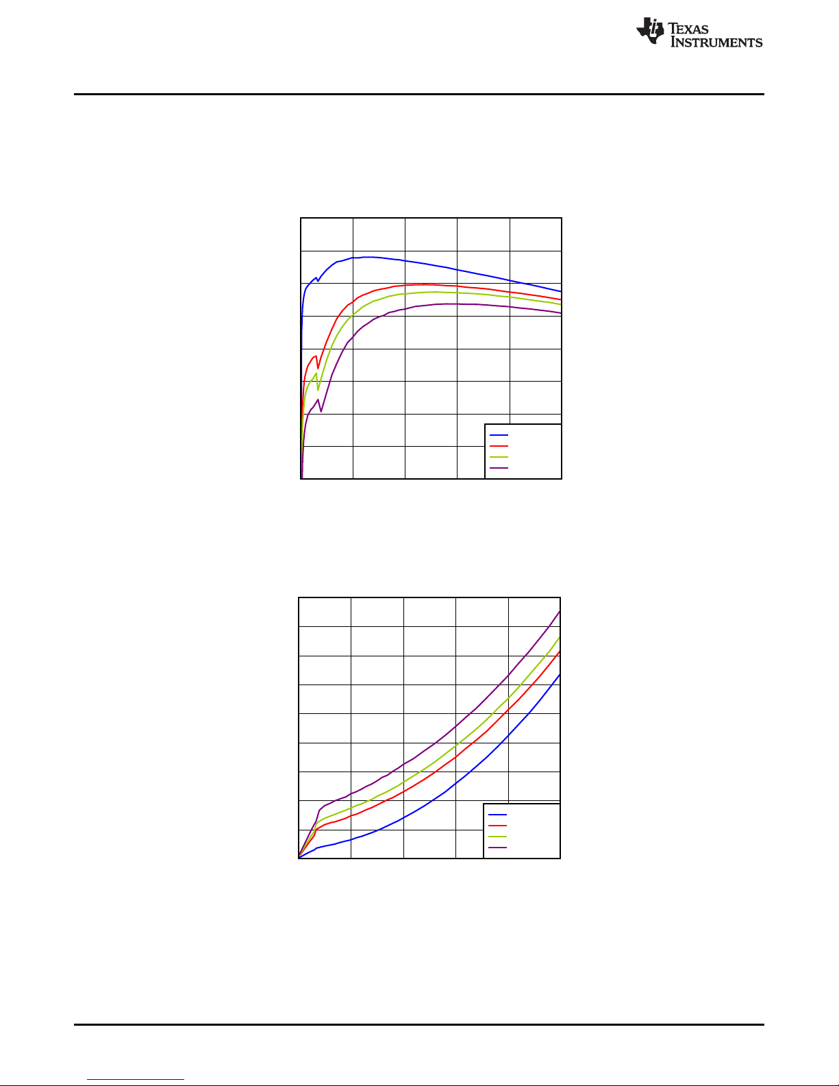
11.4 Transient Response
www.ti.com
Figure 13. Transient Response of 1-V Output at 12 VIN, Transient is 0.5 A to 15.5 A,
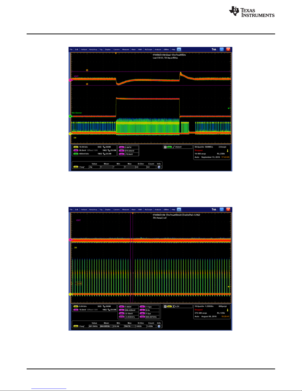
11.5 Output Ripple
the Step is 15 A at 40 A/µs
Figure 14. Output Ripple and SW Node of 1-V Output at 12 VIN, 25-A Output
18
TPS549B22EVM-847, 25-A Single Synchronous Step-Down Converter With
Full Differential Sense and PMBus™
Copyright © 2017, Texas Instruments Incorporated
Submit Documentation Feedback
SLUUBN2–March 2017
Page 19

www.ti.com
Performance Data and Typical Characteristic Curves
Figure 15. Output Ripple and SW Node of 1-V Output at 12 VIN, 0-A Output
11.6 Control On
Figure 16. Start up from Control, 1-V Output at 12 VIN, 0-A Output
SLUUBN2–March 2017
Submit Documentation Feedback
TPS549B22EVM-847, 25-A Single Synchronous Step-Down Converter With
Copyright © 2017, Texas Instruments Incorporated
Full Differential Sense and PMBus™
19
Page 20

Performance Data and Typical Characteristic Curves
Figure 17. 0.5-V Pre-bias start up from Control, 1-V Output at 12 VIN, 10-A Output
www.ti.com
11.7 Control Off
Figure 18. Start-Up and Shutdown, 1-V Output at 12 VIN, 0.5-A Output
20
TPS549B22EVM-847, 25-A Single Synchronous Step-Down Converter With
Full Differential Sense and PMBus™
Copyright © 2017, Texas Instruments Incorporated
Submit Documentation Feedback
SLUUBN2–March 2017
Page 21

www.ti.com
11.8 Thermal Image
Figure 19 illustrates the thermal image at 1-V output at 12 VIN, 25-A output, 650 kHz at 25°C ambient.
Performance Data and Typical Characteristic Curves
Figure 19. Thermal Image at 1-V Output at 12 VIN, 25-A Output, 650 kHz at 25°C Ambient
SLUUBN2–March 2017
Submit Documentation Feedback
TPS549B22EVM-847, 25-A Single Synchronous Step-Down Converter With
Copyright © 2017, Texas Instruments Incorporated
Full Differential Sense and PMBus™
21
Page 22

Fusion GUI
12 Fusion GUI
Figure 20 through Figure 23 illustrate the Fusion GUI launch and installation dialog windows.
www.ti.com
Figure 20. First Window at Fusion Launch
Figure 21. Scan Finds Device Successfully
Figure 22. Software Launch Continued
22
TPS549B22EVM-847, 25-A Single Synchronous Step-Down Converter With
Full Differential Sense and PMBus™
Figure 23. Software Launch Continued
Copyright © 2017, Texas Instruments Incorporated
Submit Documentation Feedback
SLUUBN2–March 2017
Page 23

www.ti.com
Use the All Config tab to configure all of the configurable parameters (Figure 24). The screen also shows
other details like hexadecimal (hex) encoding. Use this screen to configure:
• Power Good Delay
• Power On Delay
• Mode Settings
• Frequency, RAMP, DCAP3
• VDD UVLO
• On/Off Configuration
• Track and Sequencing
• Write Protect
• VOUT Command Voltage
• VOUT Margin
• Operation
Fusion GUI
Figure 24. First Screen After Successful Launch
SLUUBN2–March 2017
Submit Documentation Feedback
Configure: Limits and On/Off
TPS549B22EVM-847, 25-A Single Synchronous Step-Down Converter With
Copyright © 2017, Texas Instruments Incorporated
Full Differential Sense and PMBus™
23
Page 24

Fusion GUI
Changing the frequency prompts a pop-up window with details of the options Figure 25).
www.ti.com
Figure 25. Configure: Frequency- FS Configuration Pop-up
24
TPS549B22EVM-847, 25-A Single Synchronous Step-Down Converter With
Full Differential Sense and PMBus™
Copyright © 2017, Texas Instruments Incorporated
Submit Documentation Feedback
SLUUBN2–March 2017
Page 25

www.ti.com
After a change is selected, orange U icon is displayed to offer Undo Change option. Change is not
retained until either Write to Hardware or Store Config to NVM is selected. When Write to Hardware is
selected, change is committed to volatile memory and defaults back to previous setting on input power
cycle. When Store Config to NVM is selected, change is committed to nonvolatile memory and becomes
the new default (Figure 26).
Fusion GUI
Figure 26. Configure: Frequency- FS Config Pop-Up with Change
SLUUBN2–March 2017
Submit Documentation Feedback
TPS549B22EVM-847, 25-A Single Synchronous Step-Down Converter With
Copyright © 2017, Texas Instruments Incorporated
Full Differential Sense and PMBus™
25
Page 26
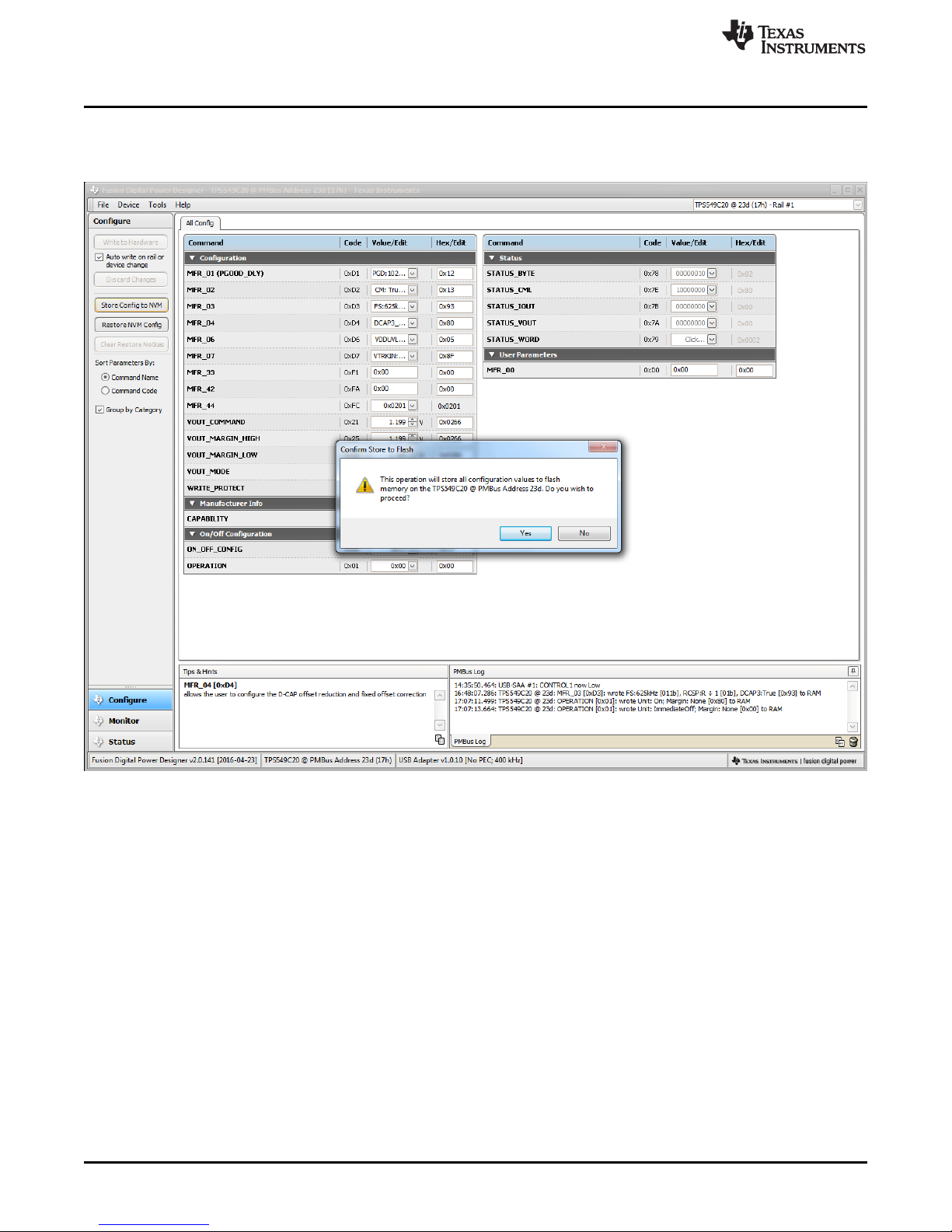
Fusion GUI
After making changes to one or more configurable parameters, the changes can be committed to
nonvolatile memory by selecting Store Config to NVM. This action prompts a confirm selection pop-up,
and if confirmed, the changes are committed to nonvolatile memory (Figure 27).
www.ti.com
26
TPS549B22EVM-847, 25-A Single Synchronous Step-Down Converter With
Full Differential Sense and PMBus™
Figure 27. Configure: Store Config to NVM
Copyright © 2017, Texas Instruments Incorporated
Submit Documentation Feedback
SLUUBN2–March 2017
Page 27
www.ti.com
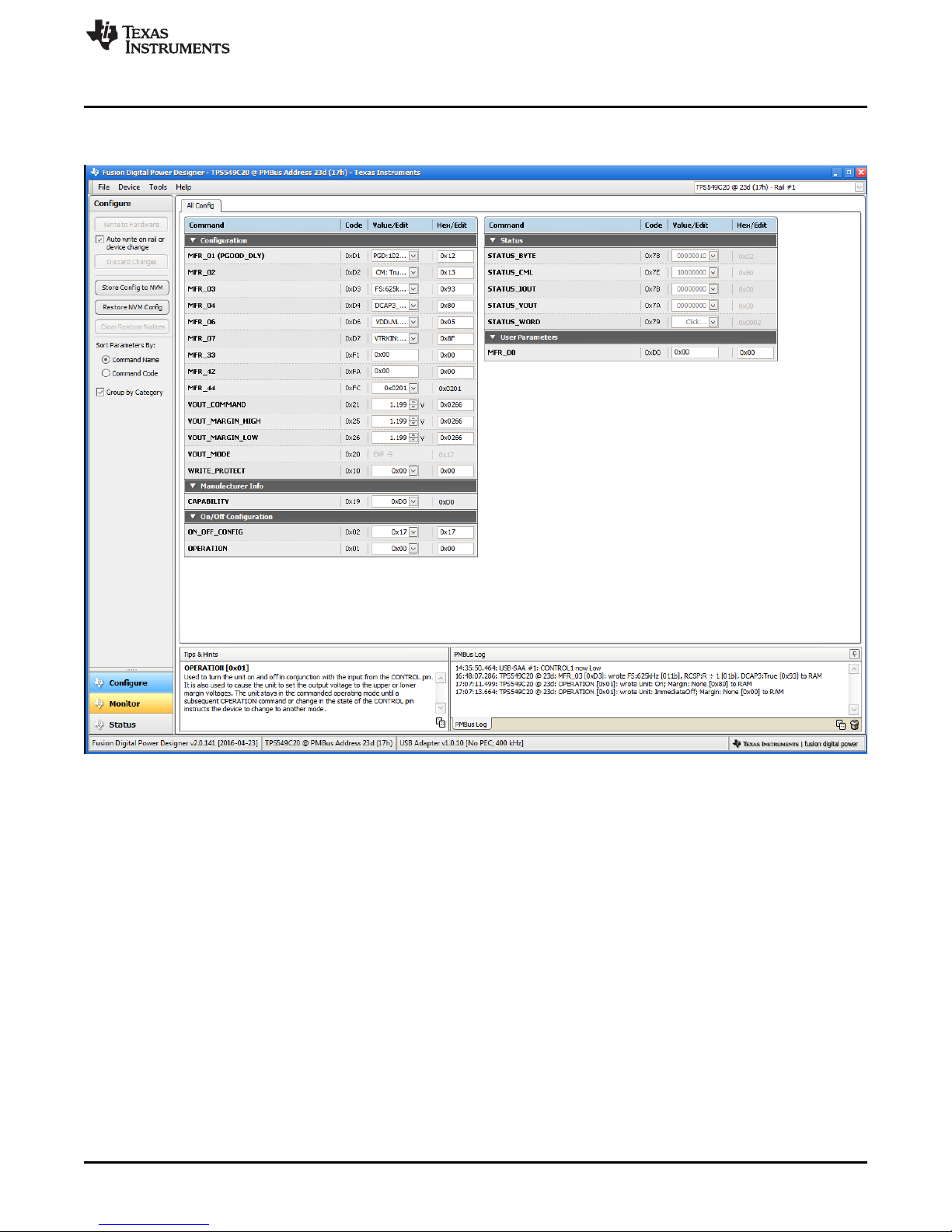
In the lower left corner, the different view screens can be changed. The view screens can be changed
between Configure, Monitor and Status as needed (Figure 28).
Fusion GUI
Figure 28. Change View Screen to Monitor Screen
SLUUBN2–March 2017
Submit Documentation Feedback
TPS549B22EVM-847, 25-A Single Synchronous Step-Down Converter With
Copyright © 2017, Texas Instruments Incorporated
Full Differential Sense and PMBus™
27
Page 28

Fusion GUI
Selecting System Dashboard from mid-left screen adds a new window which displays system-level
information (Figure 29).
www.ti.com
Figure 29. System Dashboard
28
TPS549B22EVM-847, 25-A Single Synchronous Step-Down Converter With
Full Differential Sense and PMBus™
Copyright © 2017, Texas Instruments Incorporated
Submit Documentation Feedback
SLUUBN2–March 2017
Page 29
www.ti.com
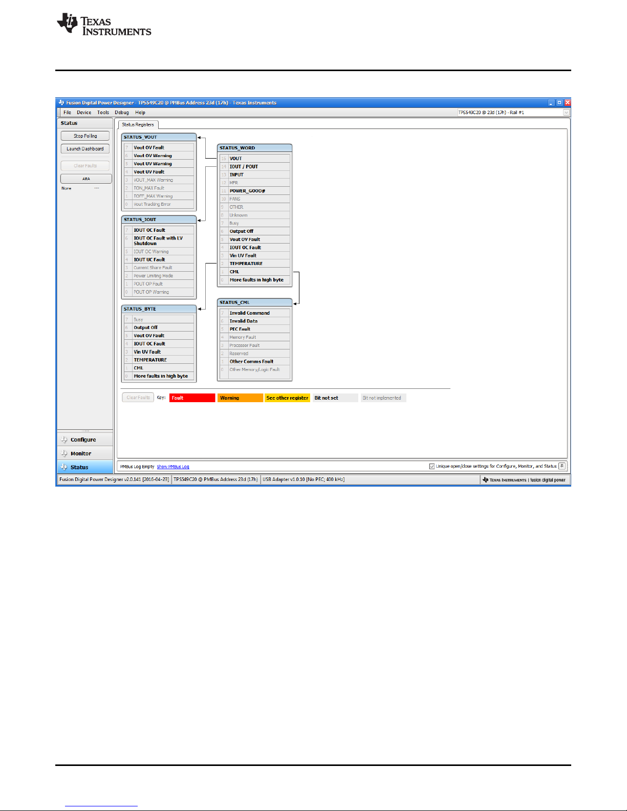
Selecting Status from lower left corner shows the status of the controller (Figure 30).
Fusion GUI
SLUUBN2–March 2017
Submit Documentation Feedback
Figure 30. Status Screen
TPS549B22EVM-847, 25-A Single Synchronous Step-Down Converter With
Copyright © 2017, Texas Instruments Incorporated
Full Differential Sense and PMBus™
29
Page 30
Fusion GUI
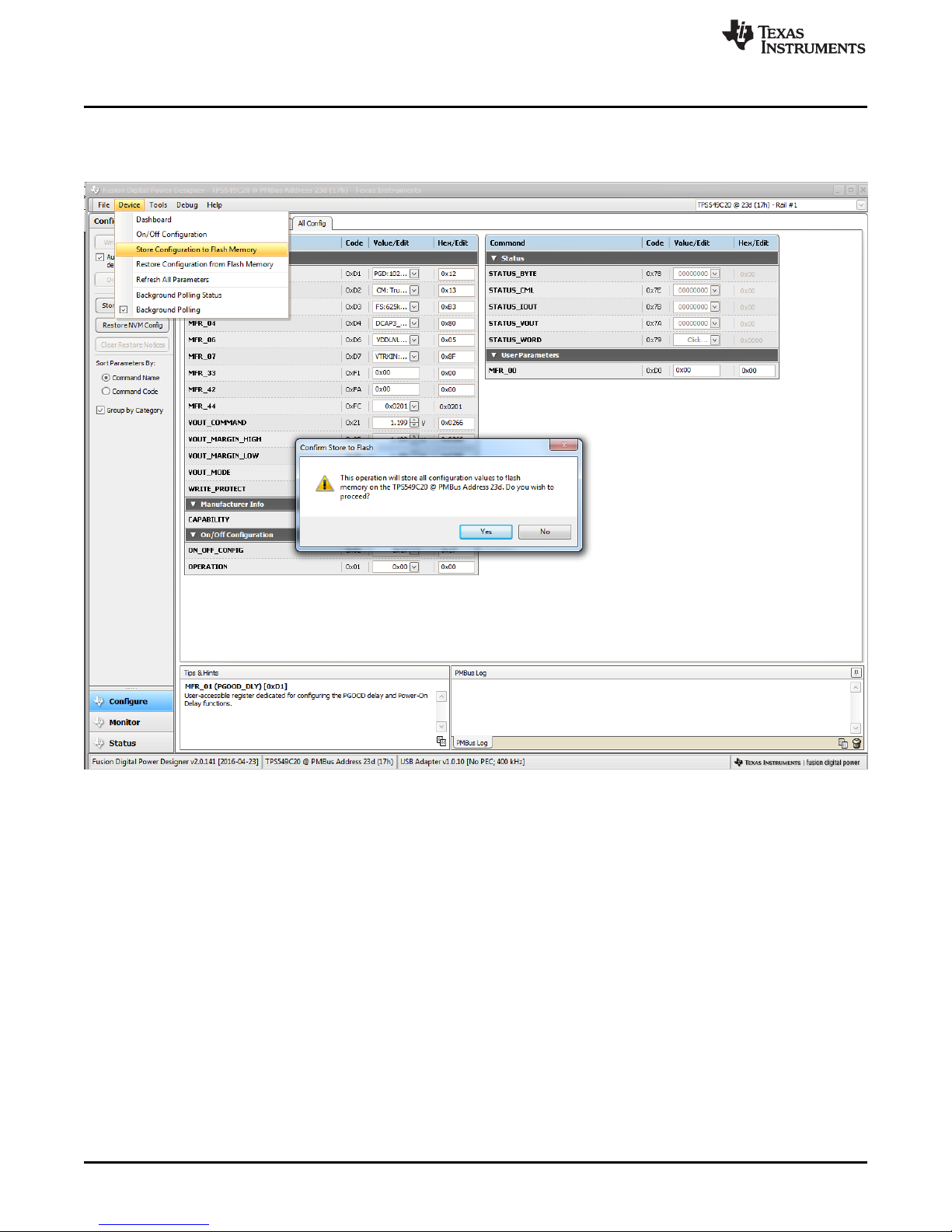
Selecting Store User Configuration to Flash Memory from the device pull-down menu has the same
functionality as the Store Config to NVM button from the configure screen. It results in committing the
current configuration to nonvolatile memory (Figure 31).
www.ti.com
Figure 31. Store Configuration To Memory
30
TPS549B22EVM-847, 25-A Single Synchronous Step-Down Converter With
Full Differential Sense and PMBus™
Copyright © 2017, Texas Instruments Incorporated
Submit Documentation Feedback
SLUUBN2–March 2017
Page 31

www.ti.com
Selecting PMBus Logging (Figure 32) from the Tools drop-down menu enables the logging of all PMBus
activity. This includes communications traffic for each polling loop between the GUI and the device. The
user is prompted to select a location for the file to be stored. See next screen (Figure 33).
Fusion GUI
SLUUBN2–March 2017
Submit Documentation Feedback
Figure 32. PMBus Logging
TPS549B22EVM-847, 25-A Single Synchronous Step-Down Converter With
Copyright © 2017, Texas Instruments Incorporated
Full Differential Sense and PMBus™
31
Page 32

Fusion GUI
Select the storage location for the file and the type of file. As shown (Figure 33), the file is a CSV file to be
stored in the directory path shown. Logging begins when the Start Logging button is selected, and stops
when it is reselected (as Stop Logging). This file can rapidly grow in size, so caution is advised when
using this function.
www.ti.com
32
TPS549B22EVM-847, 25-A Single Synchronous Step-Down Converter With
Full Differential Sense and PMBus™
Figure 33. PMBus Log Details
Copyright © 2017, Texas Instruments Incorporated
Submit Documentation Feedback
SLUUBN2–March 2017
Page 33

www.ti.com
13 EVM Assembly Drawing and PCB Layout
Figure 34 through Figure 43 show the design of the PWR-847EVM printed-circuit board (PCB). The PWR-
847EVM has a 2-oz. copper finish for all layers.
EVM Assembly Drawing and PCB Layout
Figure 34. PWR-847EVM Top Layer Assembly Drawing (Top View)
Figure 35. PWR-847EVM Top Solder Mask (Top View)
SLUUBN2–March 2017
Submit Documentation Feedback
TPS549B22EVM-847, 25-A Single Synchronous Step-Down Converter With
Copyright © 2017, Texas Instruments Incorporated
Full Differential Sense and PMBus™
33
Page 34

EVM Assembly Drawing and PCB Layout
www.ti.com
Figure 36. PWR-847EVM Top Layer (Top View)
Figure 37. PWR-847EVM Inner Layer 1 (Top View)
34
TPS549B22EVM-847, 25-A Single Synchronous Step-Down Converter With
Full Differential Sense and PMBus™
Copyright © 2017, Texas Instruments Incorporated
Submit Documentation Feedback
SLUUBN2–March 2017
Page 35

www.ti.com
EVM Assembly Drawing and PCB Layout
Figure 38. PWR-847EVM Inner Layer 2 (Top View)
Figure 39. PWR-847EVM Inner Layer 3 (Top View)
SLUUBN2–March 2017
Submit Documentation Feedback
TPS549B22EVM-847, 25-A Single Synchronous Step-Down Converter With
Copyright © 2017, Texas Instruments Incorporated
Full Differential Sense and PMBus™
35
Page 36

EVM Assembly Drawing and PCB Layout
www.ti.com
Figure 40. PWR-847EVM Inner Layer 4 (Top View)
Figure 41. PWR-847EVM Bottom Layer (Top View)
36
TPS549B22EVM-847, 25-A Single Synchronous Step-Down Converter With
Full Differential Sense and PMBus™
Copyright © 2017, Texas Instruments Incorporated
Submit Documentation Feedback
SLUUBN2–March 2017
Page 37

www.ti.com
EVM Assembly Drawing and PCB Layout
Figure 42. PWR-847EVM Bottom Solder Mask (Top View)
Figure 43. PWR-847EVM Bottom Overlay Layer (Top View)
SLUUBN2–March 2017
Submit Documentation Feedback
TPS549B22EVM-847, 25-A Single Synchronous Step-Down Converter With
Copyright © 2017, Texas Instruments Incorporated
Full Differential Sense and PMBus™
37
Page 38

List of Materials
www.ti.com
38
SLUUBN2– March 2017
Submit Documentation Feedback
Copyright © 2017, Texas Instruments Incorporated
TPS549B22EVM-847, 25-A Single Synchronous Step-Down Converter With Full
Differential Sense and PMBus™
14 List of Materials
The EVM components list, according to the schematic, is shown in Table 6.
Table 6. PWR847 List of Materials
Designator Qty Value Description Package Reference Part Number Manufacturer Alternate Part
Number
Alternate
Manufacturer
!PCB1 1 Printed Circuit Board PWR847 Any
C2, C3, C4, C5, C6,
C7, C8, C9, C13
9 22uF CAP, CERM, 22 µF, 25 V, +/- 10%, X7R, 1210 1210 GRM32ER71E226KE15L Murata
C10 1 2200pF CAP, CERM, 2200 pF, 25 V, +/- 10%, X5R, 0402 0402 GRM155R61E222KA01D Murata
C11 1 100uF CAP, AL, 100uF, 35V, +/-20%, 0.15 ohm, SMD SMT Radial G EEE-FC1V101P Panasonic
C22 1 0.1uF CAP, CERM, 0.1 µF, 50 V, +/- 10%, X7R, 0603 0603 GRM188R71H104KA93D Murata
C24, C38 2 470uF CAP, Tantalum Polymer, 470 µF, 2.5 V, +/- 20%,
0.006 ohm, 7.3x2.8x4.3mm SMD
7.3x2.8x4.3mm 2R5TPF470M6L Panasonic
C25, C26, C29, C33,
C39, C40, C42
7 100uF CAP, CERM, 100 µF, 6.3 V, +/- 20%, X5R, 1210 1210 GRM32ER60J107ME20L Murata
C35 1 1uF CAP, CERM, 1 µF, 16 V, +/- 10%, X5R, 0603 0603 C0603C105K4PACTU Kemet
C45 1 4.7uF CAP, CERM, 4.7 µF, 16 V, +/- 10%, X7R, 0805 0805 GRM21BR71C475KA73L Murata
H9, H10, H11, H12 4 Bumpon, Hemisphere, 0.44 X 0.20, Clear Transparent Bumpon SJ-5303 (CLEAR) 3M
J1, J2, J3, J5 4 TERMINAL BLOCK 5.08MM VERT 2POS, TH TERM_BLK, 2pos,
5.08mm
ED120/2DS On-Shore
Technology
J4 1 Header, 100mil, 2x1, Tin, TH Header, 2 PIN,
100mil, Tin
PEC02SAAN Sullins
Connector
Solutions
J6 1 Header (shrouded), 100mil, 5x2, Gold, TH 5x2 Shrouded header 5103308-1 TE Connectivity
L1 1 330nH Inductor, Shielded Drum Core, Ferrite, 330 nH, 50
A, 0.000165 ohm, SMD
12.5x13mm 744309033 Wurth Elektronik
LBL1 1 Thermal Transfer Printable Labels, 0.650" W x
0.200" H - 10,000 per roll
PCB Label 0.650"H x
0.200"W
THT-14-423-10 Brady
R1 1 1.00 RES, 1.00, 1%, 0.1 W, 0603 0603 RC0603FR-071RL Yageo America
R4, R7, R10, R11,
R16
5 0 RES, 0, 5%, 0.1 W, 0603 0603 CRCW06030000Z0EA Vishay-Dale
R6 1 200k RES, 200 k, 1%, 0.1 W, 0603 0603 CRCW0603200KFKEA Vishay-Dale
R8 1 1.10k RES, 1.10 k, 1%, 0.1 W, 0603 0603 CRCW06031K10FKEA Vishay-Dale
R12, R13, R20, R21,
R22
5 100k RES, 100 k, 1%, 0.1 W, 0603 0603 CRCW0603100KFKEA Vishay-Dale
R15 1 10.0k RES, 10.0k ohm, 1%, 0.1W, 0603 0603 CRCW060310K0FKEA Vishay-Dale
R19 1 61.9k RES, 61.9 k, 1%, 0.1 W, 0603 0603 CRCW060361K9FKEA Vishay-Dale
R23 1 37.4k RES, 37.4 k, 1%, 0.1 W, 0603 0603 CRCW060337K4FKEA Vishay-Dale
R24 1 42.2k RES, 42.2 k, 1%, 0.1 W, 0603 0603 CRCW060342K2FKEA Vishay-Dale
R25 1 25.5k RES, 25.5 k, 1%, 0.1 W, 0603 0603 CRCW060325K5FKEA Vishay-Dale
Page 39

www.ti.com
List of Materials
39
SLUUBN2– March 2017
Submit Documentation Feedback
Copyright © 2017, Texas Instruments Incorporated
TPS549B22EVM-847, 25-A Single Synchronous Step-Down Converter With Full
Differential Sense and PMBus™
Table 6. PWR847 List of Materials (continued)
Designator Qty Value Description Package Reference Part Number Manufacturer Alternate Part
Number
Alternate
Manufacturer
TP1, TP5, TP6, TP7,
TP8, TP9, TP12,
TP14, TP15, TP16,
TP17, TP20, TP21,
TP22
14 White Test Point, Multipurpose, White, TH White Multipurpose
Testpoint
5012 Keystone
TP2, TP3, TP4 3 Red Test Point, Multipurpose, Red, TH Red Multipurpose
Testpoint
5010 Keystone
TP10, TP11, TP13,
TP18, TP19
5 Black Test Point, Multipurpose, Black, TH Black Multipurpose
Testpoint
5011 Keystone
U1 1 1.5-V to 16-V VIN, 4.5-V to 22-V VDD, 25-A SWIFT
Synchronous Step-Down Converter with Full
Differential Sense, RVF0040A (LQFN-CLIP-40)
RVF0040A TPS549B22RVFR Texas
Instruments
TPS549B22RVFT Texas Instruments
C1, C12 0 330uF CAP, TA, 330 µF, 6.3 V, +/- 20%, 0.025 ohm, SMD 7.3x2.8x4.3mm 6TPE330ML Sanyo
C14, C15, C16, C17,
C18, C19, C20
0 22uF CAP, CERM, 22 µF, 25 V, +/- 10%, X7R, 1210 1210 GRM32ER71E226KE15L Murata
C21 0 470pF CAP, CERM, 470 pF, 50 V, +/- 10%, X7R, 0603 0603 GRM188R71H471KA01D Murata
C23, C37 0 470uF CAP, Tantalum Polymer, 470 µF, 2.5 V, +/- 20%,
0.006 ohm, 7.3x2.8x4.3mm SMD
7.3x2.8x4.3mm 2R5TPF470M6L Panasonic
C27, C28, C30, C41,
C43
0 100uF CAP, CERM, 100 µF, 6.3 V, +/- 20%, X5R, 1210 1210 GRM32ER60J107ME20L Murata
C31 0 0.1uF CAP, CERM, 0.1 µF, 50 V, +/- 10%, X7R, 0603 0603 GRM188R71H104KA93D Murata
C32 0 6800pF CAP, CERM, 6800 pF, 50 V, +/- 10%, X7R, 0603 0603 GRM188R71H682KA01D Murata
C34, C44 0 1uF CAP, CERM, 1 µF, 16 V, +/- 10%, X5R, 0603 0603 C0603C105K4PACTU Kemet
C36 0 1000pF CAP, CERM, 1000 pF, 25 V, +/- 10%, X7R, 0603 0603 GRM188R71E102KA01D Murata
C46 0 1000pF CAP, CERM, 1000 pF, 50 V, +/- 5%, C0G/NP0,
0603
0603 C0603C102J5GACTU Kemet
FID1, FID2, FID3,
FID4, FID5, FID6
0 Fiducial mark. There is nothing to buy or mount. Fiducial N/A N/A
R2, R3, R14, R17,
R18
0 0 RES, 0, 5%, 0.1 W, 0603 0603 CRCW06030000Z0EA Vishay-Dale
R5 0 1.50k RES, 1.50 k, 1%, 0.1 W, 0603 0603 RC0603FR-071K5L Yageo America
R9 0 3.01 RES, 3.01 ohm, 1%, 0.125W, 0805 0805 CRCW08053R01FKEA Vishay-Dale
Notes: Unless otherwise noted in the Alternate Part Number or Alternate Manufacturer columns, all parts may be substituted with equivalents.
Page 40

STANDARD TERMS FOR EVALUATION MODULES
1. Delivery: TI delivers TI evaluation boards, kits, or modules, including any accompanying demonstration software, components, and/or
documentation which may be provided together or separately (collectively, an “EVM” or “EVMs”) to the User (“User”) in accordance
with the terms set forth herein. User's acceptance of the EVM is expressly subject to the following terms.
1.1 EVMs are intended solely for product or software developers for use in a research and development setting to facilitate feasibility
evaluation, experimentation, or scientific analysis of TI semiconductors products. EVMs have no direct function and are not
finished products. EVMs shall not be directly or indirectly assembled as a part or subassembly in any finished product. For
clarification, any software or software tools provided with the EVM (“Software”) shall not be subject to the terms and conditions
set forth herein but rather shall be subject to the applicable terms that accompany such Software
1.2 EVMs are not intended for consumer or household use. EVMs may not be sold, sublicensed, leased, rented, loaned, assigned,
or otherwise distributed for commercial purposes by Users, in whole or in part, or used in any finished product or production
system.
2 Limited Warranty and Related Remedies/Disclaimers:
2.1 These terms do not apply to Software. The warranty, if any, for Software is covered in the applicable Software License
Agreement.
2.2 TI warrants that the TI EVM will conform to TI's published specifications for ninety (90) days after the date TI delivers such EVM
to User. Notwithstanding the foregoing, TI shall not be liable for a nonconforming EVM if (a) the nonconformity was caused by
neglect, misuse or mistreatment by an entity other than TI, including improper installation or testing, or for any EVMs that have
been altered or modified in any way by an entity other than TI, (b) the nonconformity resulted from User's design, specifications
or instructions for such EVMs or improper system design, or (c) User has not paid on time. Testing and other quality control
techniques are used to the extent TI deems necessary. TI does not test all parameters of each EVM.
User's claims against TI under this Section 2 are void if User fails to notify TI of any apparent defects in the EVMs within ten (10)
business days after delivery, or of any hidden defects with ten (10) business days after the defect has been detected.
2.3 TI's sole liability shall be at its option to repair or replace EVMs that fail to conform to the warranty set forth above, or credit
User's account for such EVM. TI's liability under this warranty shall be limited to EVMs that are returned during the warranty
period to the address designated by TI and that are determined by TI not to conform to such warranty. If TI elects to repair or
replace such EVM, TI shall have a reasonable time to repair such EVM or provide replacements. Repaired EVMs shall be
warranted for the remainder of the original warranty period. Replaced EVMs shall be warranted for a new full ninety (90) day
warranty period.
3 Regulatory Notices:
3.1 United States
3.1.1 Notice applicable to EVMs not FCC-Approved:
FCC NOTICE: This kit is designed to allow product developers to evaluate electronic components, circuitry, or software
associated with the kit to determine whether to incorporate such items in a finished product and software developers to write
software applications for use with the end product. This kit is not a finished product and when assembled may not be resold or
otherwise marketed unless all required FCC equipment authorizations are first obtained. Operation is subject to the condition
that this product not cause harmful interference to licensed radio stations and that this product accept harmful interference.
Unless the assembled kit is designed to operate under part 15, part 18 or part 95 of this chapter, the operator of the kit must
operate under the authority of an FCC license holder or must secure an experimental authorization under part 5 of this chapter.
3.1.2 For EVMs annotated as FCC – FEDERAL COMMUNICATIONS COMMISSION Part 15 Compliant:
CAUTION
This device complies with part 15 of the FCC Rules. Operation is subject to the following two conditions: (1) This device may not
cause harmful interference, and (2) this device must accept any interference received, including interference that may cause
undesired operation.
Changes or modifications not expressly approved by the party responsible for compliance could void the user's authority to
operate the equipment.
FCC Interference Statement for Class A EVM devices
NOTE: This equipment has been tested and found to comply with the limits for a Class A digital device, pursuant to part 15 of
the FCC Rules. These limits are designed to provide reasonable protection against harmful interference when the equipment is
operated in a commercial environment. This equipment generates, uses, and can radiate radio frequency energy and, if not
installed and used in accordance with the instruction manual, may cause harmful interference to radio communications.
Operation of this equipment in a residential area is likely to cause harmful interference in which case the user will be required to
correct the interference at his own expense.
Page 41

FCC Interference Statement for Class B EVM devices
NOTE: This equipment has been tested and found to comply with the limits for a Class B digital device, pursuant to part 15 of
the FCC Rules. These limits are designed to provide reasonable protection against harmful interference in a residential
installation. This equipment generates, uses and can radiate radio frequency energy and, if not installed and used in accordance
with the instructions, may cause harmful interference to radio communications. However, there is no guarantee that interference
will not occur in a particular installation. If this equipment does cause harmful interference to radio or television reception, which
can be determined by turning the equipment off and on, the user is encouraged to try to correct the interference by one or more
of the following measures:
• Reorient or relocate the receiving antenna.
• Increase the separation between the equipment and receiver.
• Connect the equipment into an outlet on a circuit different from that to which the receiver is connected.
• Consult the dealer or an experienced radio/TV technician for help.
3.2 Canada
3.2.1 For EVMs issued with an Industry Canada Certificate of Conformance to RSS-210 or RSS-247
Concerning EVMs Including Radio Transmitters:
This device complies with Industry Canada license-exempt RSSs. Operation is subject to the following two conditions:
(1) this device may not cause interference, and (2) this device must accept any interference, including interference that may
cause undesired operation of the device.
Concernant les EVMs avec appareils radio:
Le présent appareil est conforme aux CNR d'Industrie Canada applicables aux appareils radio exempts de licence. L'exploitation
est autorisée aux deux conditions suivantes: (1) l'appareil ne doit pas produire de brouillage, et (2) l'utilisateur de l'appareil doit
accepter tout brouillage radioélectrique subi, même si le brouillage est susceptible d'en compromettre le fonctionnement.
Concerning EVMs Including Detachable Antennas:
Under Industry Canada regulations, this radio transmitter may only operate using an antenna of a type and maximum (or lesser)
gain approved for the transmitter by Industry Canada. To reduce potential radio interference to other users, the antenna type
and its gain should be so chosen that the equivalent isotropically radiated power (e.i.r.p.) is not more than that necessary for
successful communication. This radio transmitter has been approved by Industry Canada to operate with the antenna types
listed in the user guide with the maximum permissible gain and required antenna impedance for each antenna type indicated.
Antenna types not included in this list, having a gain greater than the maximum gain indicated for that type, are strictly prohibited
for use with this device.
Concernant les EVMs avec antennes détachables
Conformément à la réglementation d'Industrie Canada, le présent émetteur radio peut fonctionner avec une antenne d'un type et
d'un gain maximal (ou inférieur) approuvé pour l'émetteur par Industrie Canada. Dans le but de réduire les risques de brouillage
radioélectrique à l'intention des autres utilisateurs, il faut choisir le type d'antenne et son gain de sorte que la puissance isotrope
rayonnée équivalente (p.i.r.e.) ne dépasse pas l'intensité nécessaire à l'établissement d'une communication satisfaisante. Le
présent émetteur radio a été approuvé par Industrie Canada pour fonctionner avec les types d'antenne énumérés dans le
manuel d’usage et ayant un gain admissible maximal et l'impédance requise pour chaque type d'antenne. Les types d'antenne
non inclus dans cette liste, ou dont le gain est supérieur au gain maximal indiqué, sont strictement interdits pour l'exploitation de
l'émetteur
3.3 Japan
3.3.1 Notice for EVMs delivered in Japan: Please see http://www.tij.co.jp/lsds/ti_ja/general/eStore/notice_01.page 日本国内に
輸入される評価用キット、ボードについては、次のところをご覧ください。
http://www.tij.co.jp/lsds/ti_ja/general/eStore/notice_01.page
3.3.2 Notice for Users of EVMs Considered “Radio Frequency Products” in Japan: EVMs entering Japan may not be certified
by TI as conforming to Technical Regulations of Radio Law of Japan.
If User uses EVMs in Japan, not certified to Technical Regulations of Radio Law of Japan, User is required to follow the
instructions set forth by Radio Law of Japan, which includes, but is not limited to, the instructions below with respect to EVMs
(which for the avoidance of doubt are stated strictly for convenience and should be verified by User):
1. Use EVMs in a shielded room or any other test facility as defined in the notification #173 issued by Ministry of Internal
Affairs and Communications on March 28, 2006, based on Sub-section 1.1 of Article 6 of the Ministry’s Rule for
Enforcement of Radio Law of Japan,
2. Use EVMs only after User obtains the license of Test Radio Station as provided in Radio Law of Japan with respect to
EVMs, or
3. Use of EVMs only after User obtains the Technical Regulations Conformity Certification as provided in Radio Law of Japan
with respect to EVMs. Also, do not transfer EVMs, unless User gives the same notice above to the transferee. Please note
that if User does not follow the instructions above, User will be subject to penalties of Radio Law of Japan.
Page 42

【無線電波を送信する製品の開発キットをお使いになる際の注意事項】 開発キットの中には技術基準適合証明を受けて
いないものがあります。 技術適合証明を受けていないもののご使用に際しては、電波法遵守のため、以下のいずれかの
措置を取っていただく必要がありますのでご注意ください。
1. 電波法施行規則第6条第1項第1号に基づく平成18年3月28日総務省告示第173号で定められた電波暗室等の試験設備でご使用
いただく。
2. 実験局の免許を取得後ご使用いただく。
3. 技術基準適合証明を取得後ご使用いただく。
なお、本製品は、上記の「ご使用にあたっての注意」を譲渡先、移転先に通知しない限り、譲渡、移転できないものとします。
上記を遵守頂けない場合は、電波法の罰則が適用される可能性があることをご留意ください。 日本テキサス・イ
ンスツルメンツ株式会社
東京都新宿区西新宿6丁目24番1号
西新宿三井ビル
3.3.3 Notice for EVMs for Power Line Communication: Please see http://www.tij.co.jp/lsds/ti_ja/general/eStore/notice_02.page
電力線搬送波通信についての開発キットをお使いになる際の注意事項については、次のところをご覧ください。http:/
/www.tij.co.jp/lsds/ti_ja/general/eStore/notice_02.page
3.4 European Union
3.4.1 For EVMs subject to EU Directive 2014/30/EU (Electromagnetic Compatibility Directive):
This is a class A product intended for use in environments other than domestic environments that are connected to a
low-voltage power-supply network that supplies buildings used for domestic purposes. In a domestic environment this
product may cause radio interference in which case the user may be required to take adequate measures.
4 EVM Use Restrictions and Warnings:
4.1 EVMS ARE NOT FOR USE IN FUNCTIONAL SAFETY AND/OR SAFETY CRITICAL EVALUATIONS, INCLUDING BUT NOT
LIMITED TO EVALUATIONS OF LIFE SUPPORT APPLICATIONS.
4.2 User must read and apply the user guide and other available documentation provided by TI regarding the EVM prior to handling
or using the EVM, including without limitation any warning or restriction notices. The notices contain important safety information
related to, for example, temperatures and voltages.
4.3 Safety-Related Warnings and Restrictions:
4.3.1 User shall operate the EVM within TI’s recommended specifications and environmental considerations stated in the user
guide, other available documentation provided by TI, and any other applicable requirements and employ reasonable and
customary safeguards. Exceeding the specified performance ratings and specifications (including but not limited to input
and output voltage, current, power, and environmental ranges) for the EVM may cause personal injury or death, or
property damage. If there are questions concerning performance ratings and specifications, User should contact a TI
field representative prior to connecting interface electronics including input power and intended loads. Any loads applied
outside of the specified output range may also result in unintended and/or inaccurate operation and/or possible
permanent damage to the EVM and/or interface electronics. Please consult the EVM user guide prior to connecting any
load to the EVM output. If there is uncertainty as to the load specification, please contact a TI field representative.
During normal operation, even with the inputs and outputs kept within the specified allowable ranges, some circuit
components may have elevated case temperatures. These components include but are not limited to linear regulators,
switching transistors, pass transistors, current sense resistors, and heat sinks, which can be identified using the
information in the associated documentation. When working with the EVM, please be aware that the EVM may become
very warm.
4.3.2 EVMs are intended solely for use by technically qualified, professional electronics experts who are familiar with the
dangers and application risks associated with handling electrical mechanical components, systems, and subsystems.
User assumes all responsibility and liability for proper and safe handling and use of the EVM by User or its employees,
affiliates, contractors or designees. User assumes all responsibility and liability to ensure that any interfaces (electronic
and/or mechanical) between the EVM and any human body are designed with suitable isolation and means to safely
limit accessible leakage currents to minimize the risk of electrical shock hazard. User assumes all responsibility and
liability for any improper or unsafe handling or use of the EVM by User or its employees, affiliates, contractors or
designees.
4.4 User assumes all responsibility and liability to determine whether the EVM is subject to any applicable international, federal,
state, or local laws and regulations related to User’s handling and use of the EVM and, if applicable, User assumes all
responsibility and liability for compliance in all respects with such laws and regulations. User assumes all responsibility and
liability for proper disposal and recycling of the EVM consistent with all applicable international, federal, state, and local
requirements.
5. Accuracy of Information: To the extent TI provides information on the availability and function of EVMs, TI attempts to be as accurate
as possible. However, TI does not warrant the accuracy of EVM descriptions, EVM availability or other information on its websites as
accurate, complete, reliable, current, or error-free.
Page 43

6. Disclaimers:
6.1 EXCEPT AS SET FORTH ABOVE, EVMS AND ANY MATERIALS PROVIDED WITH THE EVM (INCLUDING, BUT NOT
LIMITED TO, REFERENCE DESIGNS AND THE DESIGN OF THE EVM ITSELF) ARE PROVIDED "AS IS" AND "WITH ALL
FAULTS." TI DISCLAIMS ALL OTHER WARRANTIES, EXPRESS OR IMPLIED, REGARDING SUCH ITEMS, INCLUDING BUT
NOT LIMITED TO ANY EPIDEMIC FAILURE WARRANTY OR IMPLIED WARRANTIES OF MERCHANTABILITY OR FITNESS
FOR A PARTICULAR PURPOSE OR NON-INFRINGEMENT OF ANY THIRD PARTY PATENTS, COPYRIGHTS, TRADE
SECRETS OR OTHER INTELLECTUAL PROPERTY RIGHTS.
6.2 EXCEPT FOR THE LIMITED RIGHT TO USE THE EVM SET FORTH HEREIN, NOTHING IN THESE TERMS SHALL BE
CONSTRUED AS GRANTING OR CONFERRING ANY RIGHTS BY LICENSE, PATENT, OR ANY OTHER INDUSTRIAL OR
INTELLECTUAL PROPERTY RIGHT OF TI, ITS SUPPLIERS/LICENSORS OR ANY OTHER THIRD PARTY, TO USE THE
EVM IN ANY FINISHED END-USER OR READY-TO-USE FINAL PRODUCT, OR FOR ANY INVENTION, DISCOVERY OR
IMPROVEMENT, REGARDLESS OF WHEN MADE, CONCEIVED OR ACQUIRED.
7. USER'S INDEMNITY OBLIGATIONS AND REPRESENTATIONS. USER WILL DEFEND, INDEMNIFY AND HOLD TI, ITS
LICENSORS AND THEIR REPRESENTATIVES HARMLESS FROM AND AGAINST ANY AND ALL CLAIMS, DAMAGES, LOSSES,
EXPENSES, COSTS AND LIABILITIES (COLLECTIVELY, "CLAIMS") ARISING OUT OF OR IN CONNECTION WITH ANY
HANDLING OR USE OF THE EVM THAT IS NOT IN ACCORDANCE WITH THESE TERMS. THIS OBLIGATION SHALL APPLY
WHETHER CLAIMS ARISE UNDER STATUTE, REGULATION, OR THE LAW OF TORT, CONTRACT OR ANY OTHER LEGAL
THEORY, AND EVEN IF THE EVM FAILS TO PERFORM AS DESCRIBED OR EXPECTED.
8. Limitations on Damages and Liability:
8.1 General Limitations. IN NO EVENT SHALL TI BE LIABLE FOR ANY SPECIAL, COLLATERAL, INDIRECT, PUNITIVE,
INCIDENTAL, CONSEQUENTIAL, OR EXEMPLARY DAMAGES IN CONNECTION WITH OR ARISING OUT OF THESE
TERMS OR THE USE OF THE EVMS , REGARDLESS OF WHETHER TI HAS BEEN ADVISED OF THE POSSIBILITY OF
SUCH DAMAGES. EXCLUDED DAMAGES INCLUDE, BUT ARE NOT LIMITED TO, COST OF REMOVAL OR
REINSTALLATION, ANCILLARY COSTS TO THE PROCUREMENT OF SUBSTITUTE GOODS OR SERVICES, RETESTING,
OUTSIDE COMPUTER TIME, LABOR COSTS, LOSS OF GOODWILL, LOSS OF PROFITS, LOSS OF SAVINGS, LOSS OF
USE, LOSS OF DATA, OR BUSINESS INTERRUPTION. NO CLAIM, SUIT OR ACTION SHALL BE BROUGHT AGAINST TI
MORE THAN TWELVE (12) MONTHS AFTER THE EVENT THAT GAVE RISE TO THE CAUSE OF ACTION HAS
OCCURRED.
8.2 Specific Limitations. IN NO EVENT SHALL TI'S AGGREGATE LIABILITY FROM ANY USE OF AN EVM PROVIDED
HEREUNDER, INCLUDING FROM ANY WARRANTY, INDEMITY OR OTHER OBLIGATION ARISING OUT OF OR IN
CONNECTION WITH THESE TERMS, , EXCEED THE TOTAL AMOUNT PAID TO TI BY USER FOR THE PARTICULAR
EVM(S) AT ISSUE DURING THE PRIOR TWELVE (12) MONTHS WITH RESPECT TO WHICH LOSSES OR DAMAGES ARE
CLAIMED. THE EXISTENCE OF MORE THAN ONE CLAIM SHALL NOT ENLARGE OR EXTEND THIS LIMIT.
9. Return Policy. Except as otherwise provided, TI does not offer any refunds, returns, or exchanges. Furthermore, no return of EVM(s)
will be accepted if the package has been opened and no return of the EVM(s) will be accepted if they are damaged or otherwise not in
a resalable condition. If User feels it has been incorrectly charged for the EVM(s) it ordered or that delivery violates the applicable
order, User should contact TI. All refunds will be made in full within thirty (30) working days from the return of the components(s),
excluding any postage or packaging costs.
10. Governing Law: These terms and conditions shall be governed by and interpreted in accordance with the laws of the State of Texas,
without reference to conflict-of-laws principles. User agrees that non-exclusive jurisdiction for any dispute arising out of or relating to
these terms and conditions lies within courts located in the State of Texas and consents to venue in Dallas County, Texas.
Notwithstanding the foregoing, any judgment may be enforced in any United States or foreign court, and TI may seek injunctive relief
in any United States or foreign court.
Mailing Address: Texas Instruments, Post Office Box 655303, Dallas, Texas 75265
Copyright © 2017, Texas Instruments Incorporated
Page 44

IMPORTANT NOTICE FOR TI DESIGN INFORMATION AND RESOURCES
Texas Instruments Incorporated (‘TI”) technical, application or other design advice, services or information, including, but not limited to,
reference designs and materials relating to evaluation modules, (collectively, “TI Resources”) are intended to assist designers who are
developing applications that incorporate TI products; by downloading, accessing or using any particular TI Resource in any way, you
(individually or, if you are acting on behalf of a company, your company) agree to use it solely for this purpose and subject to the terms of
this Notice.
TI’s provision of TI Resources does not expand or otherwise alter TI’s applicable published warranties or warranty disclaimers for TI
products, and no additional obligations or liabilities arise from TI providing such TI Resources. TI reserves the right to make corrections,
enhancements, improvements and other changes to its TI Resources.
You understand and agree that you remain responsible for using your independent analysis, evaluation and judgment in designing your
applications and that you have full and exclusive responsibility to assure the safety of your applications and compliance of your applications
(and of all TI products used in or for your applications) with all applicable regulations, laws and other applicable requirements. You
represent that, with respect to your applications, you have all the necessary expertise to create and implement safeguards that (1)
anticipate dangerous consequences of failures, (2) monitor failures and their consequences, and (3) lessen the likelihood of failures that
might cause harm and take appropriate actions. You agree that prior to using or distributing any applications that include TI products, you
will thoroughly test such applications and the functionality of such TI products as used in such applications. TI has not conducted any
testing other than that specifically described in the published documentation for a particular TI Resource.
You are authorized to use, copy and modify any individual TI Resource only in connection with the development of applications that include
the TI product(s) identified in such TI Resource. NO OTHER LICENSE, EXPRESS OR IMPLIED, BY ESTOPPEL OR OTHERWISE TO
ANY OTHER TI INTELLECTUAL PROPERTY RIGHT, AND NO LICENSE TO ANY TECHNOLOGY OR INTELLECTUAL PROPERTY
RIGHT OF TI OR ANY THIRD PARTY IS GRANTED HEREIN, including but not limited to any patent right, copyright, mask work right, or
other intellectual property right relating to any combination, machine, or process in which TI products or services are used. Information
regarding or referencing third-party products or services does not constitute a license to use such products or services, or a warranty or
endorsement thereof. Use of TI Resources may require a license from a third party under the patents or other intellectual property of the
third party, or a license from TI under the patents or other intellectual property of TI.
TI RESOURCES ARE PROVIDED “AS IS” AND WITH ALL FAULTS. TI DISCLAIMS ALL OTHER WARRANTIES OR
REPRESENTATIONS, EXPRESS OR IMPLIED, REGARDING TI RESOURCES OR USE THEREOF, INCLUDING BUT NOT LIMITED TO
ACCURACY OR COMPLETENESS, TITLE, ANY EPIDEMIC FAILURE WARRANTY AND ANY IMPLIED WARRANTIES OF
MERCHANTABILITY, FITNESS FOR A PARTICULAR PURPOSE, AND NON-INFRINGEMENT OF ANY THIRD PARTY INTELLECTUAL
PROPERTY RIGHTS.
TI SHALL NOT BE LIABLE FOR AND SHALL NOT DEFEND OR INDEMNIFY YOU AGAINST ANY CLAIM, INCLUDING BUT NOT
LIMITED TO ANY INFRINGEMENT CLAIM THAT RELATES TO OR IS BASED ON ANY COMBINATION OF PRODUCTS EVEN IF
DESCRIBED IN TI RESOURCES OR OTHERWISE. IN NO EVENT SHALL TI BE LIABLE FOR ANY ACTUAL, DIRECT, SPECIAL,
COLLATERAL, INDIRECT, PUNITIVE, INCIDENTAL, CONSEQUENTIAL OR EXEMPLARY DAMAGES IN CONNECTION WITH OR
ARISING OUT OF TI RESOURCES OR USE THEREOF, AND REGARDLESS OF WHETHER TI HAS BEEN ADVISED OF THE
POSSIBILITY OF SUCH DAMAGES.
You agree to fully indemnify TI and its representatives against any damages, costs, losses, and/or liabilities arising out of your noncompliance with the terms and provisions of this Notice.
This Notice applies to TI Resources. Additional terms apply to the use and purchase of certain types of materials, TI products and services.
These include; without limitation, TI’s standard terms for semiconductor products http://www.ti.com/sc/docs/stdterms.htm), evaluation
modules, and samples (http://www.ti.com/sc/docs/sampterms.htm).
Mailing Address: Texas Instruments, Post Office Box 655303, Dallas, Texas 75265
Copyright © 2017, Texas Instruments Incorporated
 Loading...