

TEXAS INSTRUMENTS TPS54418 Technical data
100
95
90
85
80
75
70
65
60
55
50
0 0.5 1 1.5 2 2.5 3 3.5 4
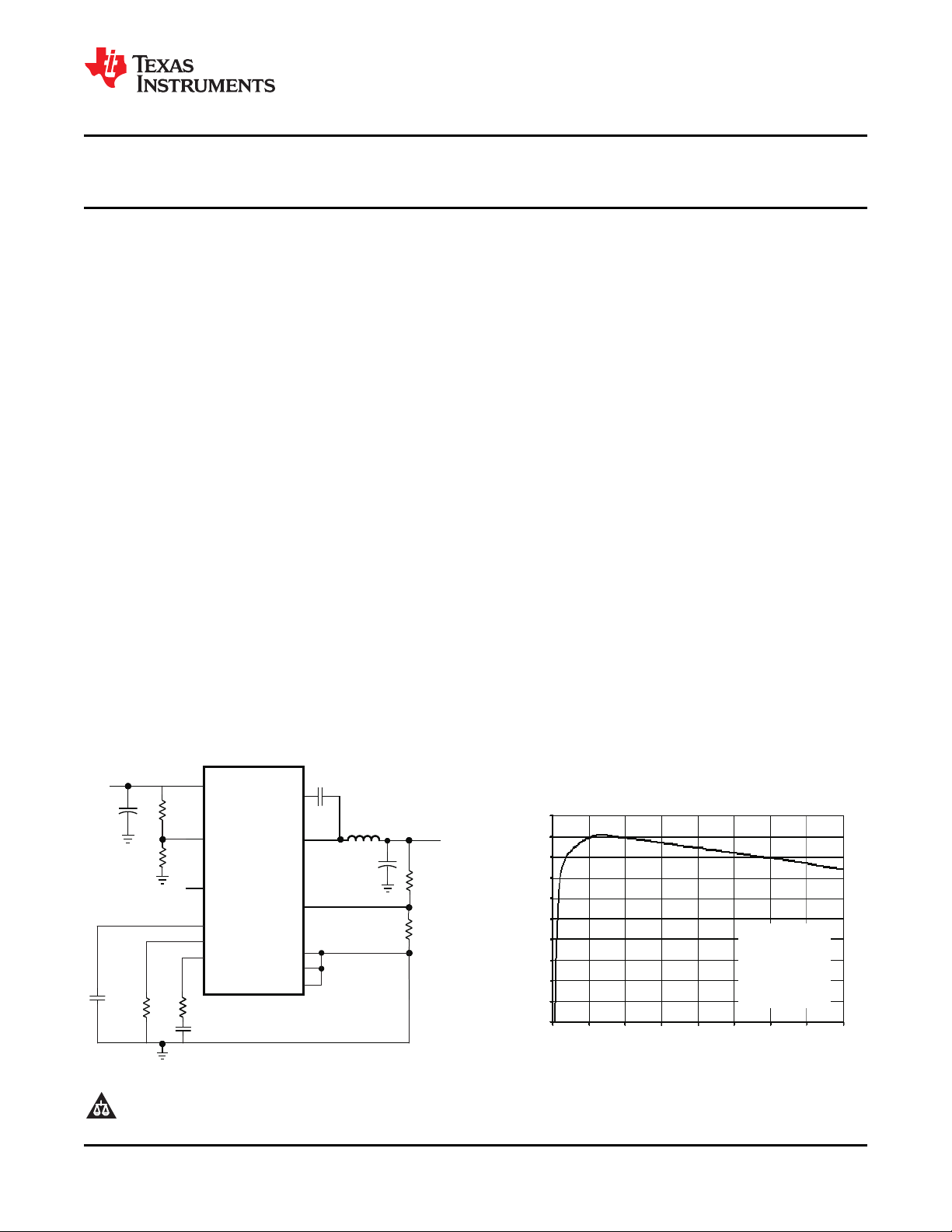
V =5V,
V =1.8V,
fsw=500kHz
IN
O
Efficiency-%
LoadCurrent- A
PH
VIN
POWERPAD
BOOT
VSENSE
COMP
TPS54418
EN
RT /CLK
SS
PWRGD
C
ss
R
T
R
3
C
1
C
BOOT
C
O
L
O
R
1
R
2
C
I
VOUT
VIN
AGND
GND
R4
R5
TPS54418
www.ti.com
........................................................................................................................................................................................................ SLVS946 – MAY 2009
2.95 V to 6 V Input, 4 A Output, 2MHz, Synchronous Step Down
Switcher With Integrated FETs ( SWIFT™)
1
FEATURES DESCRIPTION
2
• Two 30 m Ω (typical) MOSFETs for high
efficiency at 4 A loads
• 200kHz to 2MHz Switching Frequency
• 0.8 V ± 1% Voltage Reference Over
Temperature
• Synchronizes to External Clock
• Adjustable Slow Start/Sequencing
• UV and OV Power Good Output
• Low Operating and Shutdown Quiescent
Current
• Safe Start-up into Pre-Biased Output
• Cycle by Cycle Current Limit, Thermal and
Frequency Fold Back Protection
• – 40 ° C to 150 ° C Operating Junction
Temperature Range
• Thermally Enhanced 3mm × 3mm 16-pin QFN
APPLICATIONS
• Low-Voltage, High-Density Power Systems
• Point of Load Regulation for High Performance
DSPs, FPGAs, ASICs and Microprocessors
• Broadband, Networking and Optical
Communications Infrastructure
SIMPLIFIED SCHEMATIC
The TPS54418 device is a full featured 6 V, 4 A,
synchronous step down current mode converter with
two integrated MOSFETs.
The TPS54418 enables small designs by integrating
the MOSFETs, implementing current mode control to
reduce external component count, reducing inductor
size by enabling up to 2 MHz switching frequency,
and minimizing the IC footprint with a small 3mm x
3mm thermally enhanced QFN package.
The TPS54418 provides accurate regulation for a
variety of loads with an accurate ± 1% Voltage
Reference (VREF) over temperature.
Efficiency is maximized through the integrated 30m Ω
MOSFETs and 350 µ A typical supply current. Using
the enable pin, shutdown supply current is reduced to
2 µ A by entering a shutdown mode.
Under voltage lockout is internally set at 2.6 V, but
can be increased by programming the threshold with
a resistor network on the enable pin. The output
voltage startup ramp is controlled by the slow start
pin. An open drain power good signal indicates the
output is within 93% to 107% of its nominal voltage.
Frequency fold back and thermal shutdown protects
the device during an overcurrent condition.
The TPS54418 is supported in the SwitcherPro
Software Tool at www.ti.com/switcherpro .
For more SWIFT
TM
documentation, see the TI
website at www.ti.com/swift .
TM
1
2 SWIFT is a trademark of Texas Instruments.
PRODUCTION DATA information is current as of publication date.
Products conform to specifications per the terms of the Texas
Instruments standard warranty. Production processing does not
necessarily include testing of all parameters.
Please be aware that an important notice concerning availability, standard warranty, and use in critical applications of Texas
Instruments semiconductor products and disclaimers thereto appears at the end of this data sheet.
Copyright © 2009, Texas Instruments Incorporated

TPS54418
SLVS946 – MAY 2009 ........................................................................................................................................................................................................
These devices have limited built-in ESD protection. The leads should be shorted together or the device placed in conductive foam
during storage or handling to prevent electrostatic damage to the MOS gates.
www.ti.com
ORDERING INFORMATION
T
J
– 40 ° C to 150 ° C 3 × 3 mm QFN TPS54418RTE
PACKAGE PART NUMBER
ABSOLUTE MAXIMUM RATINGS
VALUE UNIT
Input voltage VIN – 0.3 to 7 V
EN – 0.3 to 7
BOOT PH + 8
VSENSE – 0.3 to 3
COMP – 0.3 to 3
PWRGD – 0.3 to 7pau
SS – 0.3 to 3
RT/CLK – 0.3 to 6
Output voltage BOOT-PH 8 V
PH – 0.6 to 7
PH 10 ns Transient – 2 to 7
Source current EN 100 µ A
RT/CLK 100 µ A
Sink current COMP 100 µ A
PWRGD 10 mA
SS 100 µ A
Electrostatic discharge (HBM) 2 kV
Electrostatic discharge (CDM) 500 V
Operating Junction temperature, T
Storage temperature, T
stg
j
– 40 to 150 ° C
– 65 to 150 ° C
PACKAGE DISSIPATION RATINGS
(1) (2) (3)
over operating free-air temperature range (unless otherwise noted)
PACKAGE
RTE 37 ° C/W 1 ° C/W
(1) Maximum power dissipation may be limited by overcurrent protection
(2) Power rating at a specific ambient temperature TAshould be determined with a junction temperature of 150 ° C. This is the point where
distortion starts to substantially increase. Thermal management of the PCB should strive to keep the junction temperature at or below
150 ° C for best performance and long-term reliability. See power dissipation estimate in application section of this data sheet for more
information.
(3) Test boards conditions:
a. 2 inches x 2 inches, 4 layers, thickness: 0.062 inch
b. 2 oz. copper traces located on the top of the PCB
c. 2 oz. copper ground planes on the 2 internal layers and bottom layer
d. 4 thermal vias (10mil) located under the device package
2 Submit Documentation Feedback Copyright © 2009, Texas Instruments Incorporated
THERMAL IMPEDANCE φJTTHERMAL CHARACTERISTIC
JUNCTION TO AMBIENT JUNCTION TO TOP
Product Folder Link(s): TPS54418
TPS54418
www.ti.com
........................................................................................................................................................................................................ SLVS946 – MAY 2009
ELECTRICAL CHARACTERISTICS
TJ= – 40 ° C to 150 ° C, VIN = 2.95 to 6 V (unless otherwise noted)
DESCRIPTION CONDITIONS MIN TYP MAX UNIT
SUPPLY VOLTAGE (VIN PIN)
Operating input voltage 2.95 6 V
Internal under voltage lockout threshold No voltage hysteresis, rising and falling 2.6 2.8 V
Shutdown supply current EN = 0 V, 25 ° C, 2.95 V ≤ VIN ≤ 6 V 2 5 µ A
Quiescent Current - I
ENABLE AND UVLO (EN PIN)
Enable threshold Rising 1.16 1.25 1.37 V
Input current µ A
VOLTAGE REFERENCE (VSENSE PIN)
Voltage Reference 2.95 V ≤ VIN ≤ 6 V, – 40 ° C < TJ< 150 ° C 0.795 0.803 0.811 V
MOSFET
High side switch resistance m Ω
Low side switch resistance m Ω
ERROR AMPLIFIER
Input current 7 nA
Error amplifier transconductance (gm) – 2 µ A < I(COMP) < 2 µ A, V(COMP) = 1 V 225 µ mhos
Error amplifier transconductance (gm) during – 2 µ A < I(COMP) < 2 µ A, V(COMP) = 1 V, 70 µ mhos
slow start Vsense = 0.4 V
Error amplifier source/sink V(COMP) = 1 V, 100 mV overdrive ± 20 µ A
COMP to Iswitch gm 13.0 A/V
CURRENT LIMIT
Current limit threshold 5.0 6.4 A
THERMAL SHUTDOWN
Thermal Shutdown 175 ° C
Hysteresis 15 ° C
TIMING RESISTOR AND EXTERNAL CLOCK (RT/CLK PIN)
Switching frequency range using RT mode 200 2000 kHz
Switching frequency Rt = 400 k Ω 400 500 600 kHz
Switching frequency range using CLK mode 300 2000 kHz
Minimum CLK pulse width 75 ns
RT/CLK voltage R(RT/CLK)= 400k Ω 0.5 V
RT/CLK high threshold 1.6 2.2 V
RT/CLK low threshold 0.4 0.6 V
RT/CLK falling edge to PH rising edge delay Measure at 500 kHz with RT resistor in series 90 ns
PLL lock in time Measure at 500 kHz 14 µ s
PH (PH PIN)
Minimum On time Measured at 50% points on PH, IOUT = 4 A 60 ns
Minimum Off time Prior to skipping off pulses, BOOT-PH = 2.95 V, 60 ns
Rise/Fall Time VIN = 5 V 1.5 V/ns
q
VSENSE = 0.9 V, VIN = 5 V, 25 ° C, RT = 400 k Ω 350 500 µ A
Falling 1.18
Enable threshold + 50 mV -3.2
Enable threshold – 50 mV -0.65
BOOT-PH= 5 V 30 60
BOOT-PH= 2.95 V 44 70
VIN= 5 V 30 60
VIN= 2.95 V 44 70
Measured at 50% points on PH, VIN = 5 V, IOUT = 0 110
A
IOUT = 4 A
Copyright © 2009, Texas Instruments Incorporated Submit Documentation Feedback 3
Product Folder Link(s): TPS54418
TPS54418
SLVS946 – MAY 2009 ........................................................................................................................................................................................................
www.ti.com
ELECTRICAL CHARACTERISTICS (continued)
TJ= – 40 ° C to 150 ° C, VIN = 2.95 to 6 V (unless otherwise noted)
DESCRIPTION CONDITIONS MIN TYP MAX UNIT
BOOT (BOOT PIN)
BOOT Charge Resistance VIN = 5 V 16 Ω
BOOT-PH UVLO VIN = 2.95 V 2.1 V
SLOW START (SS PIN)
Charge Current V(SS) = 0.4 V 1.8 µ A
SS to reference crossover 98% nominal 0.9 V
SS discharge voltage (overload) VSENSE = 0 V 20 µ A
SS discharge current (UVLO, EN, Thermal VIN = 5 V, V(SS) = 0.5 V 1.25 mA
Fault)
POWER GOOD (PWRGD PIN)
VSENSE falling (Fault) 91 % Vref
VSENSE threshold
Hysteresis VSENSE falling 2 % Vref
Output high leakage VSENSE = VREF, V(PWRGD) = 5.5 V 2 nA
On resistance 100 Ω
Output low I(PWRGD) = 3.5 mA 0.3 V
Minimum VIN for valid output V(PWRGD) < 0.5 V at 100 µ A 1.2 1.6 V
VSENSE rising (Good) 93 % Vref
VSENSE rising (Fault) 107 % Vref
VSENSE falling (Good) 105 % Vref
4 Submit Documentation Feedback Copyright © 2009, Texas Instruments Incorporated
Product Folder Link(s): TPS54418
PWRGD
BOOT
PH
RT/CLK
EN
AGND
VIN
VSENSE
COMP
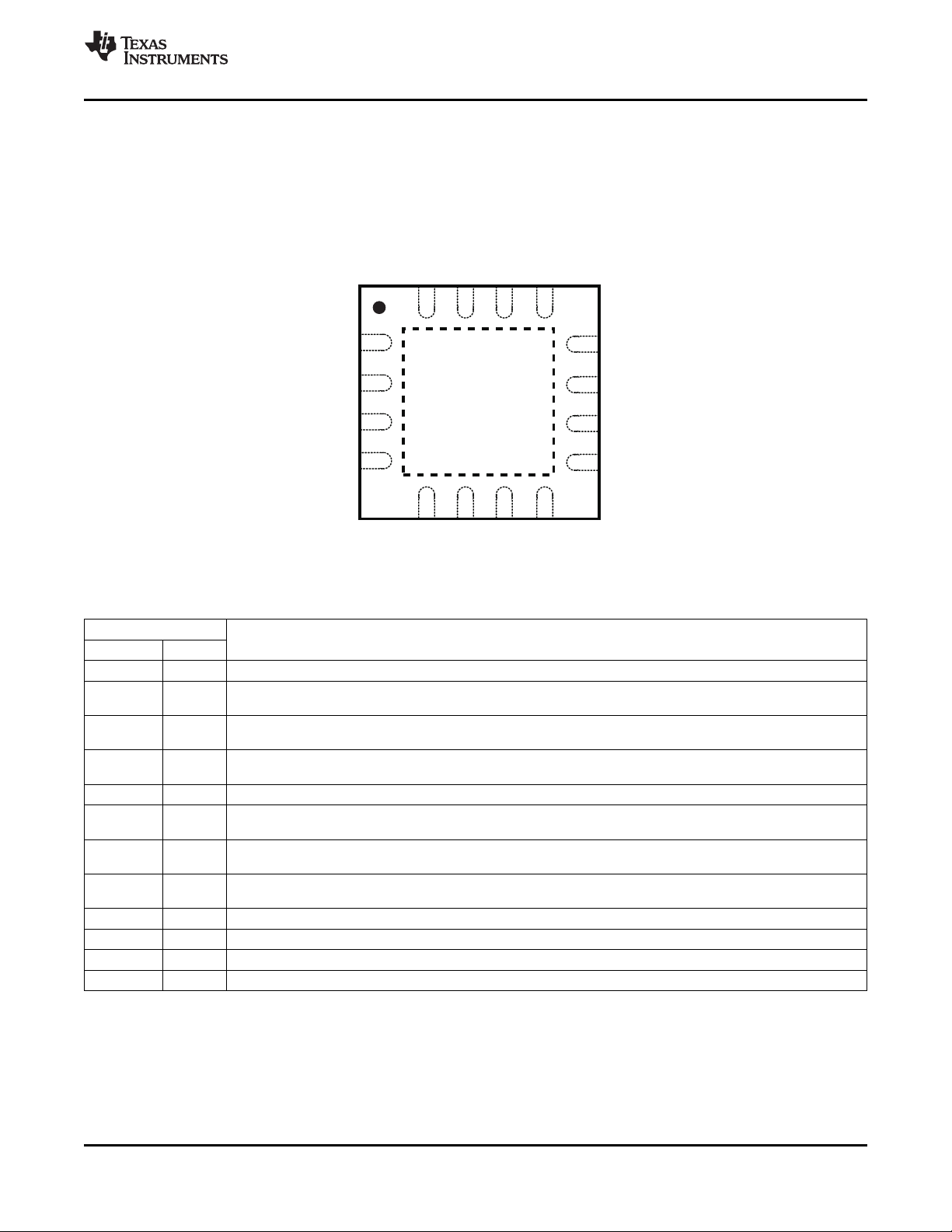
15 14 13
GND
12
11
10
9
8
765
16
GND
VIN
VIN
PH
PH
1
2
3
4
SS
Thermal
Pad
(17)
QFN16
RTEPACKAGE
(TOP VIEW)
TPS54418
www.ti.com
........................................................................................................................................................................................................ SLVS946 – MAY 2009
DEVICE INFORMATION
PIN CONFIGURATION
PIN FUNCTIONS
PIN
NAME NO.
AGND 5 Analog Ground should be electrically connected to GND close to the device.
BOOT 13 A bootstrap capacitor is required between BOOT and PH. If the voltage on this capacitor is below the minimum
required by the BOOT UVLO, the output is forced to switch off until the capacitor is refreshed.
COMP 7 Error amplifier output, and input to the output switch current comparator. Connect frequency compensation
components to this pin.
EN 15 Enable pin, internal pull-up current source. Pull below 1.2 V to disable. Float to enable. Can be used to set the
on/off threshold (adjust UVLO) with two additional resistors.
GND 3, 4 Power Ground. This pin should be electrically connected directly to the power pad under the IC.
PH 10, 11, The source of the internal high side power MOSFET, and drain of the internal low side (synchronous) rectifier
12 MOSFET.
PowerPAD 17 GND pin should be connected to the exposed power pad for proper operation. This power pad should be
connected to any internal PCB ground plane using multiple vias for good thermal performance.
PWRGD 14 An open drain output, asserts low if output voltage is low due to thermal shutdown, overcurrent,
over/under-voltage or EN shut down.
RT/CLK 8 Resistor Timing or External Clock input pin.
SS 9 Slow-start. An external capacitor connected to this pin sets the output voltage rise time.
VIN 1, 2, 16 Input supply voltage, 2.95 V to 6 V.
VSENSE 6 Inverting node of the transconductance (gm) error amplifier.
DESCRIPTION
Copyright © 2009, Texas Instruments Incorporated Submit Documentation Feedback 5
Product Folder Link(s): TPS54418
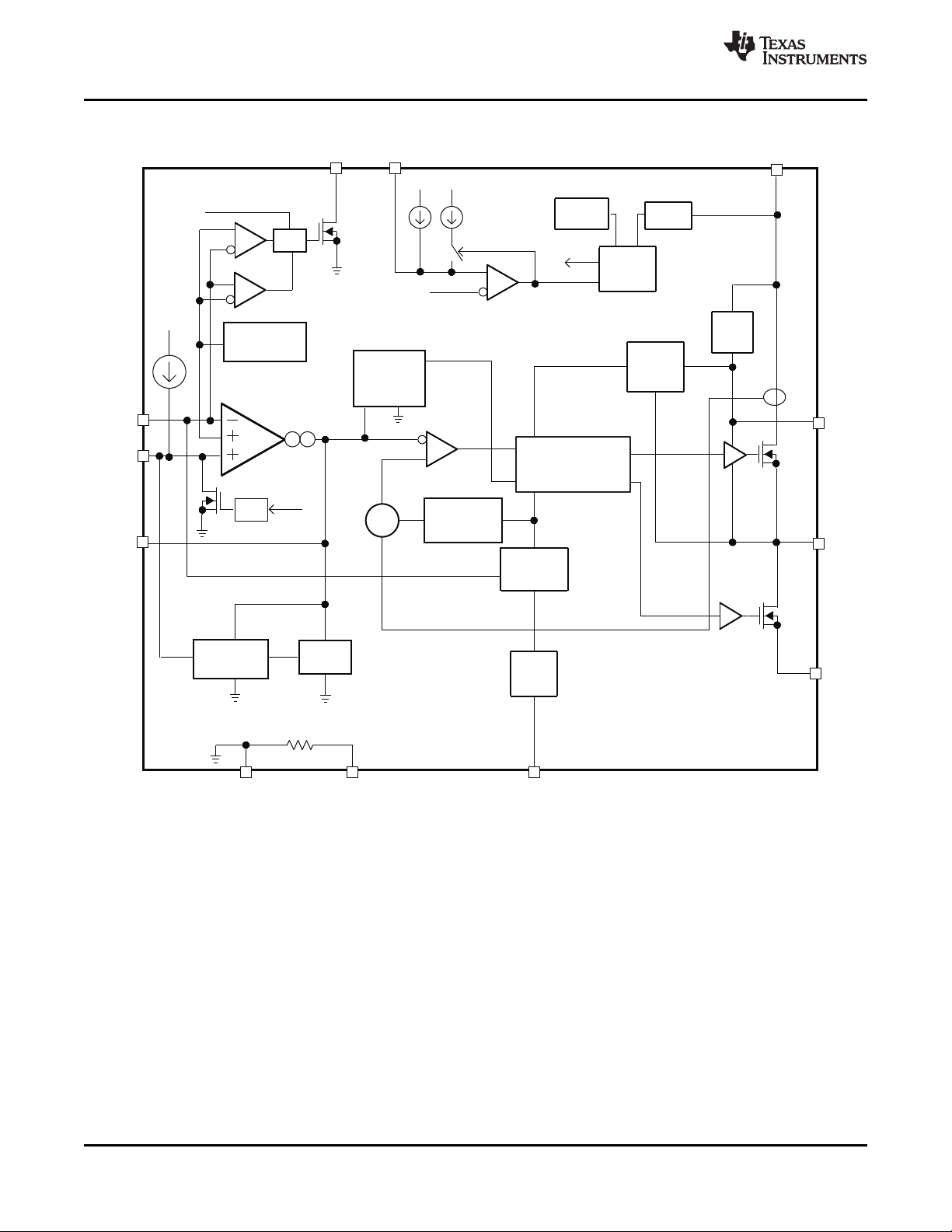
ERROR
AMPLIFIER
Boot
Charge
Boot
UVLO
UVLO
Current
Sense
Oscillator
withPLL
Frequency
Shift
Slope
Compensation
PWM
Comparator
Minimum
COMP Clamp
Maximum
Clamp
Voltage
Reference
Overload
Recovery
VSENSE
SS
COMP
RT/CLK
PH
BOOT
VIN
AGND
Thermal
Shutdown
EN
Enable
Comparator
Shutdown
Logic
Shutdown
Enable
Threshold
TPS54418RTEBlockDiagram
Logic
Shutdown
PWRGD
POWERPAD
GND
Logic
Shutdown
107%
93%
S
LogicandPWM
Latch
i
1
i
hys
TPS54418
SLVS946 – MAY 2009 ........................................................................................................................................................................................................
FUNCTIONAL BLOCK DIAGRAM
www.ti.com
6 Submit Documentation Feedback Copyright © 2009, Texas Instruments Incorporated
Product Folder Link(s): TPS54418

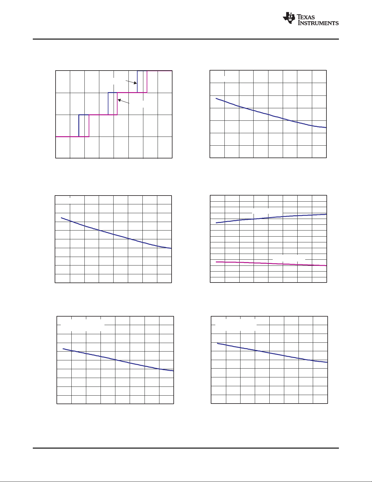
450
460
470
480
490
500
510
520
530
540
550
f
-SwitchingFrequency-kHz
s
-50 -25 0 25 50 75 100 125 150
T -JunctionTemperature-°C
J
RT =400k ,
V =3.3V
W
I
0.02
0.025
0.03
0.035
0.04
0.045
0.05
0.055
-50 -25 0 25 50 75 100 125 150
T -JunctionTemperature-°C
J
HighSideRdson
V =3.3V
I
HighSideRdson
V =5V
I
LowSideRdson
V =3.3V
I
LowSideRdson
V =5V
I
RDSON-StaticDrain-SourceOn-StateResistance-
W
-50 -25 0 25 50 75 100 125 150
T -JunctionTemperature-°C
J
V =3V
IN
6
6.1
6.2
6.3
6.4
6.5
6.6
6.7
6.8
6.9
7
HighSideSwitchCurrent- A
0.792
0.794
0.796
0.798
0.8
0.802
0.804
0.806
0.808
-50 -25 0 25 50 75 100 125 150
T -JunctionTemperature-°C
J
V -VoltageReference-V
ref
V =3.3V
IN
1000
1100
1200
1300
1400
1500
1600
1700
1800
1900
2000
80 100 120 140 160 180 200
RT-ResistancekW
f
-SwitchingFrequency-KHz
s
200
300
400
500
600
700
800
900
1000
100 200 300 400 500 600 700 800 900 1000
RT-Resistance-kW
f -
SwitchingFrequncy-KHz
s
TPS54418
www.ti.com
........................................................................................................................................................................................................ SLVS946 – MAY 2009
TYPICAL CHARACTERISTICS CURVES
HIGH SIDE AND LOW SIDE Rdson vs TEMPERATURE FREQUENCY vs TEMPERATURE
Figure 1. Figure 2.
HIGH SIDE CURRENT LIMIT vs TEMPERATURE VOLTAGE REFERENCE vs TEMPERATURE
Figure 3. Figure 4.
SWITCHING FREQUENCY vs RT RESISTANCE LOW SWITCHING FREQUENCY vs RT RESISTANCE HIGH
FREQUENCY RANGE FREQUENCY RANGE
Copyright © 2009, Texas Instruments Incorporated Submit Documentation Feedback 7
Figure 5. Figure 6.
Product Folder Link(s): TPS54418
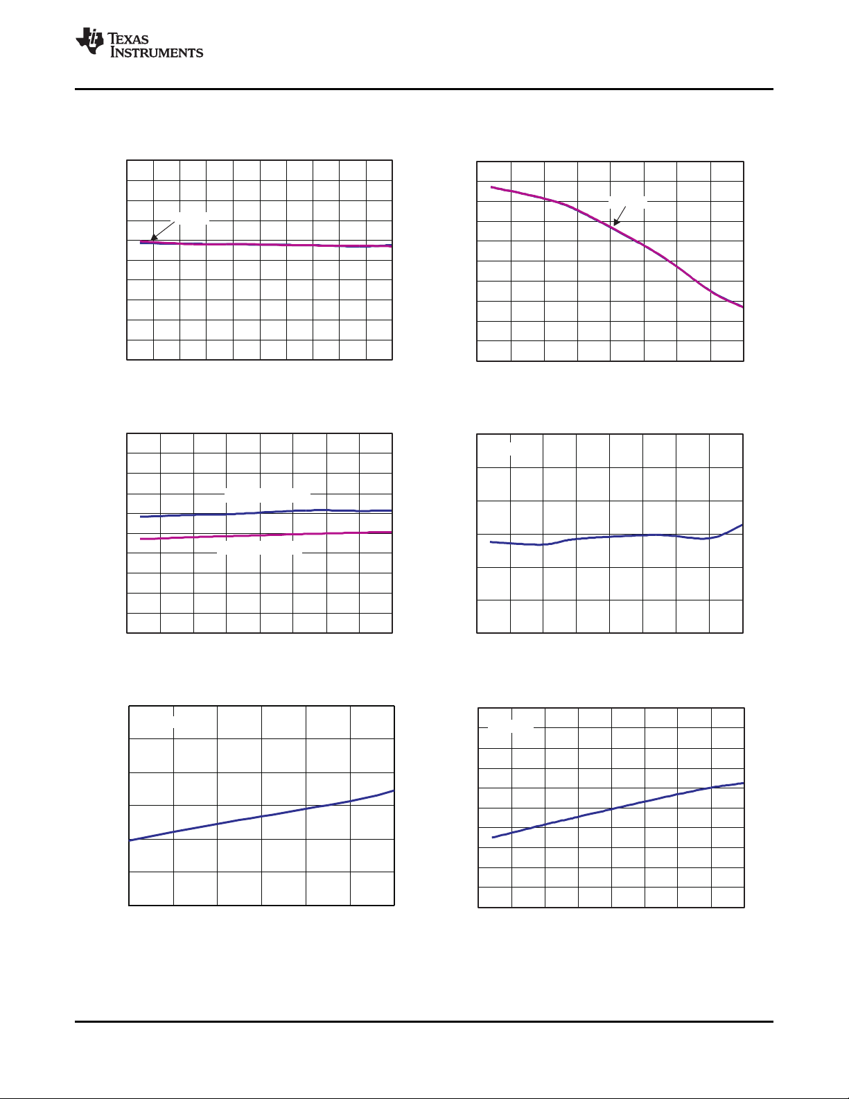
0
25
50
75
100
0 0.1 0.2 0.3 0.4 0.5 0.6 0.7 0.8
Vsense-V
VsenseFalling
VsenseRising
NormalSwitchingFrequency-%
140
160
180
200
220
240
260
280
-50 -25 0 25 50 75 100 125 150
T -JunctionTemperature-°C
J
V =3.3V
IN
EA
-Transconductance- A/Vm
1.15
1.16
1.17
1.18
1.19
1.2
1.21
1.22
1.23
1.24
1.25
1.26
1.27
1.28
1.29
1.3
-50 -25 0 25 50 75 100 125 150
T -JunctionTemperature-°C
J
V =3.3V,rising
IN
V =3.3V,falling
IN
EN-Threshold-V
40
45
50
55
60
65
70
75
80
85
90
-50 -25 0 25 50 75 100 125 150
T -JunctionTemperature-°C
J
V =3.3V
IN
EA
-Transconductance- A/Vm
EN PinCurrent- Am-
-3.75
-3.65
-3.55
-3.45
-3.35
-3.25
-3.15
-3.05
-2.95
-2.85
-2.75
-50 -25 0 25 50 75 100 125 150
T -JunctionTemperature-°C
J
V =5V,
Ien= Threshold+50mV
IN
EN-PinCurrent- Am
-1.25
-1.15
-1.05
-0.95
-0.85
-0.75
-0.65
-0.55
-0.45
-0.35
-0.25
-50 -25 0 25 50 75 100 125 150
T -JunctionTemperature-°C
J
V =5V,
Ien= Threshold-50mV
IN
TPS54418
SLVS946 – MAY 2009 ........................................................................................................................................................................................................
www.ti.com
TYPICAL CHARACTERISTICS CURVES (continued)
SWITHING FREQUENCY vs VSENSE TRANSCONDUCTANCE vs TEMPERATURE
Figure 7. Figure 8.
TRANSCONDUCTANCE (SLOW START) vs JUNCTION
TEMPERATURE ENABLE PIN VOLTAGE vs TEMPERATURE
Figure 9. Figure 10.
PIN CURRENT vs TEMPERATURE PIN CURRENT vs TEMPERATURE
8 Submit Documentation Feedback Copyright © 2009, Texas Instruments Incorporated
Figure 11. Figure 12.
Product Folder Link(s): TPS54418
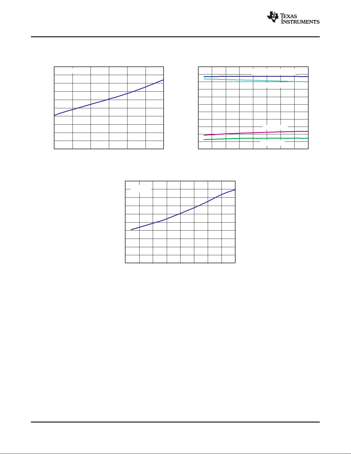
SS/TR-ChargeCurrent- Am
-3
-2.8
-2.6
-2.4
-2.2
-2
-1.8
-1.6
-1.4
-1.2
-1
V =5V
IN
-50 -25 0 25 50 75 100 125 150
T -JunctionTemperature-°C
J
SS/TR-DischargeCurrent- Am
85
87
89
91
93
95
97
99
101
103
105
V =5V
IN
-50 -25 0 25 50 75 100 125 150
T -JunctionTemperature-°C
J
V
-InputV
oltage-V
IN
2
2.1
2.2
2.3
2.4
2.5
2.6
2.7
2.8
2.9
3
-50 -25 0 25 50 75 100 125 150
T -JunctionTemperature-°C
J
UVLOStartSwitching
UVLOStopSwitching
0
0.5
1
1.5
2
2.5
3
-50 -25 0 25 50 75 100 125 150
T -JunctionTemperature-°C
J
ShutdownSupplyCurrent- Am
V =3.3V
IN
ShutdownSupplyCurrent Am
0
0.5
1
1.5
2
2.5
3
3 3.5 4 4.5 5 5.5 6
V -InputVoltage-V
IN
T =25°C
J
300
310
320
330
340
350
360
370
380
390
400
V =3.3V
IN
I -SupplyCurrent- A
CC
m
-50 -25 0 25 50 75 100 125 150
T -JunctionTemperature-°C
J
TPS54418
www.ti.com
........................................................................................................................................................................................................ SLVS946 – MAY 2009
TYPICAL CHARACTERISTICS CURVES (continued)
CHARGE CURRENT vs TEMPERATURE DISCHARGE CURRENT vs TEMPERATURE
Figure 13. Figure 14.
INPUT VOLTAGE vs TEMPERATURE SHUTDOWN SUPPLY CURRENT vs TEMPERATURE
Figure 15. Figure 16.
SHUTDOWN SUPPLY CURRENT vs INPUT VOLTAGE SUPPLY CURRENT vs TEMPERATURE
Copyright © 2009, Texas Instruments Incorporated Submit Documentation Feedback 9
Figure 17. Figure 18.
Product Folder Link(s): TPS54418
I -SupplyCurrent- A
CC
m
300
310
320
330
340
350
360
370
380
390
400
3 3.5 4 4.5 5 5.5 6
V -InputVoltage-V
IN
T =25°C
J
PWRGD-Threshold-%V
r
ef
88
90
92
94
96
98
100
102
104
106
108
110
VsenseRising,V =3.3V
IN
VsenseRising
VsenseFalling
VsenseFalling
-50 -25 0 25 50 75 100 125 150
T -JunctionTemperature-°C
J
RDSON-StaticDrain-SourecOnStateResistance- W
0
20
40
60
80
100
120
140
160
180
200
-50 -25 0 25 50 75 100 125 150
T -JunctionTemperature-°C
J
V =3.3V
IN
TPS54418
SLVS946 – MAY 2009 ........................................................................................................................................................................................................
www.ti.com
TYPICAL CHARACTERISTICS CURVES (continued)
SUPPLY CURRENT vs INPUT VOLTAGE PWRGD THRESHOLD vs TEMPERATURE
Figure 19. Figure 20.
PWRGD ON RESISTANCE vs TEMPERATURE
OVERVIEW
The TPS54418 is a 6-V, 4-A, synchronous step-down (buck) converter with two integrated n-channel MOSFETs.
To improve performance during line and load transients the device implements a constant frequency, peak
current mode control which reduces output capacitance and simplifies external frequency compensation design.
The wide switching frequency of 200 kHz to 2000 kHz allows for efficiency and size optimization when selecting
the output filter components. The switching frequency is adjusted using a resistor to ground on the RT/CLK pin.
The device has an internal phase lock loop (PLL) on the RT/CLK pin that is used to synchronize the power
switch turn on to a falling edge of an external system clock.
The TPS54418 has a typical default start up voltage of 2.6 V. The EN pin has an internal pull-up current source
that can be used to adjust the input voltage under voltage lockout (UVLO) with two external resistors. In addition,
the pull up current provides a default condition when the EN pin is floating for the device to operate. The total
operating current for the TPS54418 is 350 µ A when not switching and under no load. When the device is
disabled, the supply current is less than 5 µ A.
The integrated 30 m Ω MOSFETs allow for high efficiency power supply designs with continuous output currents
up to 4 amperes.
10 Submit Documentation Feedback Copyright © 2009, Texas Instruments Incorporated
Figure 21.
Product Folder Link(s): TPS54418

TPS54418
www.ti.com
........................................................................................................................................................................................................ SLVS946 – MAY 2009
The TPS54418 reduces the external component count by integrating the boot recharge diode. The bias voltage
for the integrated high side MOSFET is supplied by a capacitor on the BOOT to PH pin. The boot capacitor
voltage is monitored by an UVLO circuit and turns off the high side MOSFET when the voltage falls below a
preset threshold. This BOOT circuit allows the TPS54418 to operate approaching 100%. The output voltage can
be stepped down to as low as the 0.8 V reference.
The TPS54418 has a power good comparator (PWRGD) with 2% hysteresis.
The TPS54418 minimizes excessive output overvoltage transients by taking advantage of the overvoltage power
good comparator. When the regulated output voltage is greater than 109% of the nominal voltage, the
overvoltage comparator is activated, and the high side MOSFET is turned off and masked from turning on until
the output voltage is lower than 105%.
The SS (slow start) pin is used to minimize inrush currents or provide power supply sequencing during power up.
A small value capacitor should be coupled to the pin for slow start. The SS pin is discharged before the output
power up to ensure a repeatable restart after an over-temperature fault, UVLO fault or disabled condition.
The use of a frequency foldback circuit reduces the switching frequency during startup and over current fault
conditions to help limit the inductor current.
DETAILED DESCRIPTION
FIXED FREQUENCY PWM CONTROL
The TPS54418 uses an adjustable fixed frequency, peak current mode control. The output voltage is compared
through external resistors on the VSENSE pin to an internal voltage reference by an error amplifier which drives
the COMP pin. An internal oscillator initiates the turn on of the high side power switch. The error amplifier output
is compared to the high side power switch current. When the power switch current reaches the COMP voltage
level the high side power switch is turned off and the low side power switch is turned on. The COMP pin voltage
increases and decreases as the output current increases and decreases. The device implements a current limit
by clamping the COMP pin voltage to a maximum level and also implements a minimum clamp for improved
transient response performance.
SLOPE COMPENSATION AND OUTPUT CURRENT
The TPS54418 adds a compensating ramp to the switch current signal. This slope compensation prevents
sub-harmonic oscillations as duty cycle increases. The available peak inductor current remains constant over the
full duty cycle range.
BOOTSTRAP VOLTAGE (BOOT) AND LOW DROPOUT OPERATION
The TPS54418 has an integrated boot regulator and requires a small ceramic capacitor between the BOOT and
PH pin to provide the gate drive voltage for the high side MOSFET. The value of the ceramic capacitor should be
0.1 µ F. A ceramic capacitor with an X7R or X5R grade dielectric with a voltage rating of 10 V or higher is
recommended because of the stable characteristics over temperature and voltage.
To improve drop out, the TPS54418 is designed to operate at 100% duty cycle as long as the BOOT to PH pin
voltage is greater than 2.5 V. The high side MOSFET is turned off using an UVLO circuit, allowing for the low
side MOSFET to conduct when the voltage from BOOT to PH drops below 2.5 V. Since the supply current
sourced from the BOOT pin is very low, the high side MOSFET can remain on for more switching cycles than are
required to refresh the capacitor, thus the effective duty cycle of the switching regulator is very high.
ERROR AMPLIFIER
The TPS54418 has a transconductance amplifier. The error amplifier compares the VSENSE voltage to the lower
of the SS pin voltage or the internal 0.8 V voltage reference. The transconductance of the error amplifier is 225
µ A/V during normal operation. When the voltage of VSENSE pin is below 0.8 V and the device is regulating
using the SS voltage, the gm is 70 µ A/V. The frequency compensation components are placed between the
COMP pin and ground.
Copyright © 2009, Texas Instruments Incorporated Submit Documentation Feedback 11
Product Folder Link(s): TPS54418
 Loading...