

Page 1
1 Introduction
The Texas Instruments TPS54362BEVM evaluation module (EVM) helps designers evaluate the operation
and performance of the TPS54362B-Q1 switch-mode power-supply buck regulator. The device is
configurable and can be configured to switch from 200 kHz up to 2.2 MHz. This EVM is optimized for EMI
performance. For the EMI test results, see the application report Passing CISPR25 Radiated Emissions
Using TPS54362B-Q1, SLVA661.
CONVERTER IC PACKAGE
U1 TPS54362BQPWPQ1 PWP-20
EVM INPUT VOLTAGE RANGE DEFAULT OUTPUT SETTING
TPS54362BEVM VI= 3.6 V to 40 V 5 V at currents up to 3 A
User's Guide
SLVUA81–May 2014
TPS54362B EVM User’s Guide
Table 1. Device and Package Configurations
Table 2. Input and Output Summary
1.1 Performance Summary
The TPS54362BEVM is optimized to meet the CISPR25 EMC standard for automotive components.
TPS54362BEVM was tested at V
reduce emissions to levels deemed acceptable by the previously mentioned standard.
The switching frequency is externally set at a nominal 500 KHz. The compensation components are
external to the integrated circuit (IC) and have been selected to optimize the transient performance of the
device. An external divider allows for an adjustable output voltage.
Table 3 lists a summary of the TPS54362BEVM performance specifications. Specifications are given for
an input voltage of VI= 12 V and an output voltage of 5 V, unless otherwise specified. The
TPS54362BEVM is designed and tested for VI= 6 V to 48 V. The ambient temperature is 25°C for all
measurements, unless otherwise noted.
Table 3. TPS54362BEVM Performance Specification Summary
SPECIFICATION TEST CONDITION MIN TYP MAX UNIT
VIN operating voltage range 6 12 48 V
Output voltage set-point 5 V
Output current range VI= 7 V to 48 V 0 3 A
Operating frequency 500 kHz
= 12 V an output voltage of 5 V at 2 A. The layout is designed to
(BAT)
SLVUA81–May 2014 TPS54362B EVM User’s Guide
Submit Documentation Feedback
Copyright © 2014, Texas Instruments Incorporated
1
Page 2

ENA ENA
Disabled Enabled
LPM
Disabled
LPM
Enabled
LPM
Disabled with
Protection Diode
Setup
2 Setup
This section describes the jumpers and connectors on the EVM as well and how to properly connect, set
up, and use the TPS54362BEVM.
2.1 Input-Output Connector Description
J1 – Input — This jumper is the power input terminal for the converter. The terminal block provides a
power (V
harness.
J2 – Output — This jumper is the regulated output voltage for the converter. The terminal block provides
a power (VO) and ground (GND) connection to allow the user to attach the EVM to a cable harness.
J3 – Sync — This jumper is the input terminal for an optional external input clock to the converter. The
external clock can be used to synchronize the switching frequency for multiple devices. The
external clock frequency, if used, must meet the guideline as shown in Equation 1.
ƒS< ƒ
where
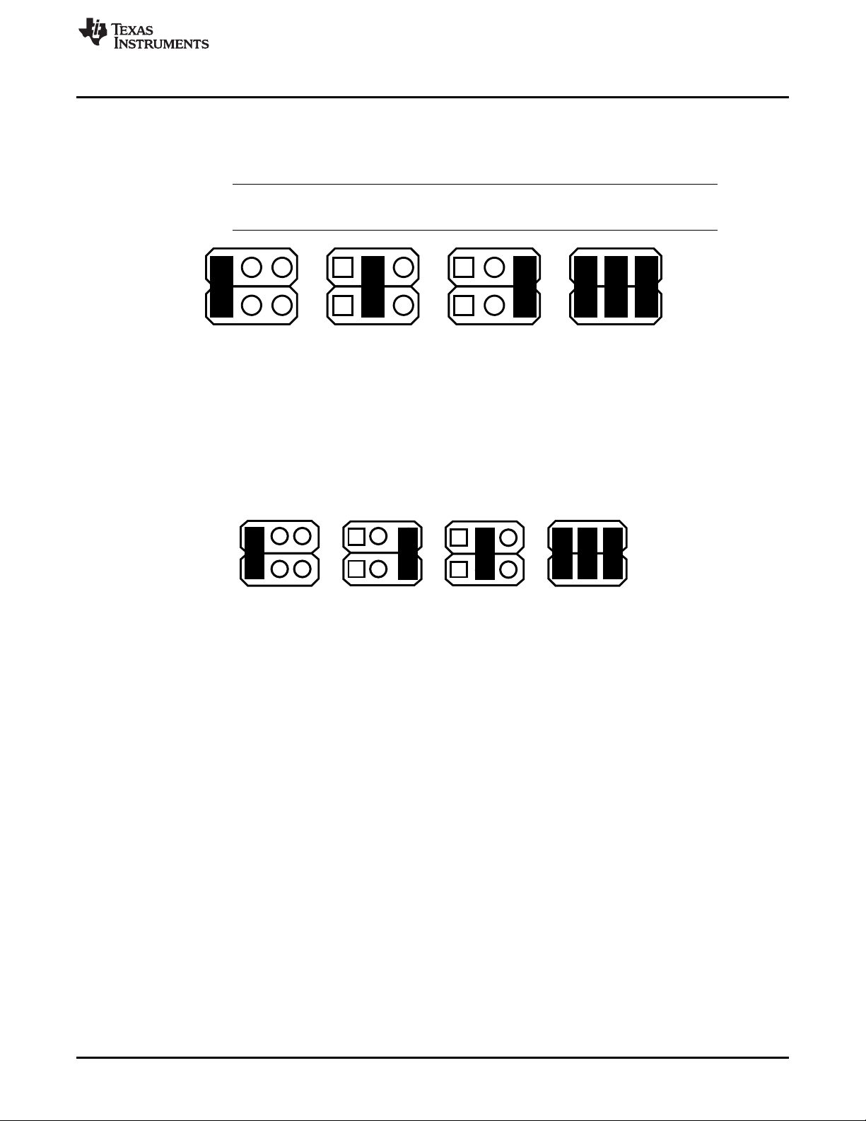
JP1 – LPM — This jumper is the jumper used to enable Low Power Mode. The jumper allows LPM to be
enabled or disabled. The “disabled with protection diode” selection should be used if the output
voltage is programmed for voltages greater than 5 V. The external Zener will prevent over voltage
damage to the LPM input.
) and ground (GND) connection to allow the user to attach the EVM to a cable
(BAT)
< 2 × ƒ
(EXT)
• ƒSis the switching frequency (1)
S
www.ti.com
JP2 – Enable—The converter is enabled when the EN pin is high and is disabled when the EN pin is low.
The jumper placement allows the converter to be enabled or disabled.
2
TPS54362B EVM User’s Guide SLVUA81–May 2014
Figure 2. Enable Jumper Settings
Copyright © 2014, Texas Instruments Incorporated
Figure 1. LPM Jumper Settings
Submit Documentation Feedback
Page 3
Delay
7 ms
50 ms 150 ms 200 ms
Delay Delay Delay
SR SR SR SR
1 V, 2.5 ns
1 V, 4 ns 1 V, 6 ns
1 V, 1.2 ns
www.ti.com
JP3 – Slew Rate — This jumper sets the slew rate for the switch pin. The device slew rate should be set
JP4 – Delay — This jumper sets the delay time to assert the RST pin low after the supply exceeds the
Setup
between 15 ns and 200 ns. Slower slew rates can improve EMI performance, but increase
switching losses. Jumper resistors allow the slew rate to be set to four set points. The user can set
a specific slew rate by changing one of the slew rate set resistors, either R8, R9, or R10.
NOTE: The slew rate should be set to 1 V, 1.2 ns if the EVM is configured for a 2-MHz
switching frequency.
Figure 3. Slew-Rate Jumper Settings
programmed VREG_RST voltage. The delay can be programmed in the range of 7 ms to 200 ms.
Jumper capacitors allow the reset delay to be set to four set points. The user can set a specific
delay time by changing one of the delay capacitors, either C13, C14, or C15. The RST signal can
be monitored on the RST test point.
Figure 4. Reset Delay-Time Jumper Settings
2.2 Setup
The input voltage range for the converter is 3.6 V to 48 V. If the input voltage is lower than 5 V (default
setting) the output voltage will track the input voltage within the drop out proportional to the load current
and the internal FET on resistance.
2.3 Operation
For proper operation of the TPS54362B-Q1 device, JP1, JP2, JP3, and JP4 should be properly
configured. The following lists the recommended setting which uses shorting blocks:
• JP1 to enabled
• JP2 to enabled
• JP3 to 1 V, 2.5 ns
• JP4 to 200 ms
In this configuration, the device powers up when power is applied.
Setting the R6 and R7 resistors to transition the EN input low as the supply voltage drops implements
undervoltage lockout. Use Equation 2 to set the values for R6 and R7.
V
= ENTHRES × (1+ R6 / R7)
dis
where
SLVUA81–May 2014 TPS54362B EVM User’s Guide
Submit Documentation Feedback
Copyright © 2014, Texas Instruments Incorporated
3
Page 4
Board Layout
• ENTHRES is around 1 V (2)
Resistor R7 is not populated on this EVM to reduce the quiescent supply current if this feature is not
required.
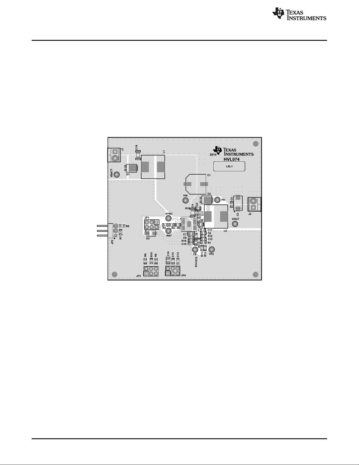
3 Board Layout
Figure 5, Figure 6, Figure 7, Figure 8, and Figure 9 show the board layout for the TPS54362BEVM PWB.
The EVM offers resistors, capacitors, and jumpers to program the switch-pin slew rate and regulator turnon delay. Jumpers are also provided to enable the device and to enable the low power-mode option. The
TPS54362B-Q1 converter offers high efficiency, but dissipates power. The PowerPAD™ package offers
an exposed thermal pad to enhance thermal performance. This pad must be soldered to the copper
landing on the PCB for optimal performance. The PCB provides 2-oz copper planes on the top and bottom
to dissipate heat.
www.ti.com
Figure 5. Top Assembly Layer
4
TPS54362B EVM User’s Guide SLVUA81–May 2014
Copyright © 2014, Texas Instruments Incorporated
Submit Documentation Feedback
Page 5

www.ti.com
Board Layout
Figure 6. Top Layer Routing Figure 7. Inner Layer 2 (Ground Plane)
Figure 8. Inner Layer 3 Routing Figure 9. Bottom Layer (Ground Plane)
SLVUA81–May 2014 TPS54362B EVM User’s Guide
Submit Documentation Feedback
Copyright © 2014, Texas Instruments Incorporated
5
Page 6

22µH
L1
VBat
60V
D1
220µF
C1
GND
NC
1
NC
2
SYNC
3
LPM
4
EN
5
RT
6
RSLEW
7
RST
8
CDLY
9
GND
10
SS
11
OV_TH
12
RST_TH
13
VSENSE
14
COMP
15
VREG
16
PH
17
VIN
18
VIN
19
BOOT
20
PWRPAD
21
U1
TPS54362QPWPRQ1
GND
GND
22µH
L2
GND
60V
D2
GND
R7
DNP
GND
GND
220pF
C12
GND
2200pF
C13
15.0k
R16
GND
GND
GND
SYNC
1
2
J1
1
2
J2
PH
RST FB
VOUT
VIN VBATT
GND
GND
VIN
(2)
V REG
0.15µF
C7
100µF
C3
0.15µF
C14
22pF
C8
2.55k
R13
49.9
R11
82.5k
R14
22pF
C10
GNDGND
V REG
30.1k
R8
330pF
C9
0.1µF
C6
22pF
C11
274k
R12
35.7k
R2
187k
R1
0.1µF
C5
47.0k
R10
1µF
C4
GND
0.1µF
C2
V REG
0.047µF
C15
2.00k
R4
68.1k
R9
V REG
30.1k
R6
221k
R3
GND
30.1k
R5
12345
6
JP3
EN
V REG
GND
GND
12345
6
JP1
GND
GND
1
2
3
JP2
12345
6
JP4
4.7µF
C16
GND
0
R17
1500pF
C17
GND
DNP
VIN
INPUT
GND
OUT
(1)
GND
VBAT
GND
10.0
R18
5.1V
D3
SMAZ5V1-13-F
TP2
2.26k
R15
Schematic and Bill of Materials
4 Schematic and Bill of Materials
4.1 Schematic
www.ti.com
Submit Documentation Feedback
(1) Output voltage = 5 V, load current = 3 A maximum
(2) Input voltage up to 48 V
6
TPS54362B EVM User’s Guide SLVUA81–May 2014
Figure 10. Schematic
Copyright © 2014, Texas Instruments Incorporated
Page 7

www.ti.com
4.2 Bill of Materials
Schematic and Bill of Materials
Table 4. TPS54362BEVM Bill of Materials for a 500-kHz Configuration
DESIGNATOR QUANTITY VALUE DESCRIPTION PACKAGE PART NUMBER MANUFACTURER ALTERNATE PART ALTERNATE
!PCB 1 Printed Circuit Board TPS54362BEVM Any - C1 1 220 µF Capacitor, AL, 220 µF, 50 V, SMT Radial G EEE-FK1H221P Panasonic
±20%, 0.18 Ω, SMD
C2, C5, C6 3 0.1 µF Capacitor, ceramic, 0.1 µF, 50 V, 0603 GRM188R71H104KA93D MuRata
±10%, X7R, 0603
C3 1 100 µF Capacitor, TA, 100 µF, 16 V, 7343-31 TPSD107M016R0060 AVX
±20%, 0.06 Ω, SMD
C4 1 1 µF Capacitor, ceramic, 1 µF, 50 V, 1206 GRM31MR71H105KA88L MuRata
±10%, X7R, 1206
C7, C14 2 0.15 µF Capacitor, ceramic, 0.15 µF, 25 V, 0805 08053C154KAT2A AVX
±10%, X7R, 0805
C8, C10, C11 3 22 pF Capacitor, ceramic, 22 pF, 50 V, 0603 06035A220JAT2A AVX
±5%, C0G/NP0, 0603
C9 1 330 pF Capacitor, ceramic, 330 pF, 50 V, 0603 C0603C331J5GACTU Kemet
±5%, C0G/NP0, 0603
C12 1 220 pF Capacitor, ceramic, 220 pF, 50 V, 0603 C1608C0G1H221J TDK
±5%, C0G/NP0, 0603
C13 1 2200 pF Capacitor, ceramic, 2200 pF, 50 V, 0603 GRM1885C1H222JA01D MuRata
±5%, C0G/NP0, 0603
C15 1 0.047 µF Capacitor, ceramic, 0.047 µF, 50 0603 C1608X7R1H473K TDK
V, ±10%, X7R, 0603
C16 1 4.7 µF Capacitor, ceramic, 4.7 µF, 50 V, 1206 GRM31CR71H475KA12L MuRata
±10%, X7R, 1206
C17 1 1500 pF Capacitor, ceramic, 1500 pF, 50 V, 0603 GRM188R71H152KA01D MuRata
±10%, X7R, 0603
D1, D2 2 60 V Diode, Schottky, 60 V, 3 A, PowerDI5 PDS360-13 Diodes Inc.
PowerDI5
D3 1 5.1 V Diode, Zener, 5.1 V, 1 W, SMA SMA SMAZ5V1-13-F Diodes Inc.
FB, PH, RST, SYNC, 8 Red Test Point, Miniature, Red, TH Red Miniature 5000 Keystone
TP2, VBATT, VIN, Testpoint
VOUT
J1, J2 2 Terminal Block, 6 A, 3.5 mm Pitch, 7.0x8.2x6.5mm ED555/2DS On-Shore
2-Pos, TH Technology
JP1, JP3, JP4 3 Header, 100 mil, 3 × 2, Tin, TH 3x2 Header PEC03DAAN Sullins Connector
JP2 1 Header, male, 3 × 1, 100 mil, RA, Header, 3x1, PEC03SBAN Sullins Connector
TH RA Solutions
L1, L2 2 22 µH Inductor, Shielded Drum Core, MSS1278T MSS1278T-223MLB Coilcraft
Ferrite, 22 µH, 4 A, 0.04 Ω, SMD
REFERENCE NUMBER MANUFACTURER
Solutions
SLVUA81–May 2014 TPS54362B EVM User’s Guide
Submit Documentation Feedback
Copyright © 2014, Texas Instruments Incorporated
7
Page 8

Schematic and Bill of Materials
www.ti.com
Table 4. TPS54362BEVM Bill of Materials for a 500-kHz Configuration (continued)
DESIGNATOR QUANTITY VALUE DESCRIPTION PACKAGE PART NUMBER MANUFACTURER ALTERNATE PART ALTERNATE
LBL1 1 Thermal Transfer Printable Labels, PCB Label THT-14-423-10 Brady - -
R1 1 187 kΩ Resistor, 187 kΩ, 1%, 0.1 W, 0603 0603 RC0603FR-07187KL YageoAmerica
R2 1 35.7 kΩ Resistor, 35.7 kΩ, 1%, 0.1 W, 0603 CRCW060335K7FKEA Vishay-Dale
R3 1 221 kΩ Resistor, 221 kΩ, 1%, 0.1 W, 0603 0603 RC0603FR-07221KL YageoAmerica
R4 1 2 kΩ Resistor, 2.00 kΩ, 1%, 0.1 W, 0603 CRCW06032K00FKEA Vishay-Dale
R5, R6, R8 3 30.1 kΩ Resistor, 30.1 kΩ, 1%, 0.1 W, 0603 CRCW060330K1FKEA Vishay-Dale
R9 1 68.1 kΩ Resistor, 68.1 kΩ, 1%, 0.1 W, 0603 CRCW060368K1FKEA Vishay-Dale
R10 1 47 kΩ Resistor, 47 kΩ, 1%, 0.1 W, 0603 0603 RC0603FR-0747KL Yageo America
R11 1 49.9 Ω Resistor, 49.9 Ω, 1%, 0.1 W, 0603 0603 CRCW060349R9FKEA Vishay-Dale
R12 1 274 kΩ Resistor, 274 kΩ, 1%, 0.1 W, 0603 0603 CRCW0603274KFKEA Vishay-Dale
R13 1 2.55 kΩ Resistor, 2.55 kΩ, 1%, 0.1 W, 0603 CRCW06032K55FKEA Vishay-Dale
R14 1 82.5 kΩ Resistor, 82.5 kΩ, 1%, 0.1 W, 0603 CRCW060382K5FKEA Vishay-Dale
R15 1 2.26 kΩ Resistor, 2.26 kΩ, 1%, 0.1 W, 0603 CRCW06032K26FKEA Vishay-Dale
R16 1 15 kΩ Resistor, 15.0 kΩ, 1%, 0.1 W, 0603 CRCW060315K0FKEA Vishay-Dale
R17 1 0 Ω Resistor, 0 Ω, 5%, 0.1 W, 0603 0603 CRCW06030000Z0EA Vishay-Dale
R18 1 10 Ω Resistor, 10 Ω, 1%, 0.1 W, 0603 0603 RC0603FR-0710RL Yageo America
SH-JP1A, SH-JP1B, 10 1× 2 Shunt, 100 mil, Gold plated, Black Shunt 969102-0000-DA 3M SNT-100-BK-G Samtec
SH-JP1C, SH-JP2,
SH-JP3A, SH-JP3B,
SH-JP3C, SH-JP4A,
SH-JP4B, SH-JP4C
U1 1 TPS54362BQP IC, 3 A, 60 V step down DC/DC PWP20 TPS54362BQPWPRQ1 TI None
WPRQ1 converter with low I
FID1, FID2, FID3 0 Fiducial mark. There is nothing to Fiducial N/A N/A
R7 0 0 Resistor, 0 Ω, 5%, 0.1 W, 0603 0603 CRCW06030000Z0EA Vishay-Dale
0.650" W x 0.200" H - 10,000 per 0.650"H x
roll 0.200"W
0603
0603
0603
0603
0603
0603
0603
0603
Q
buy or mount.
REFERENCE NUMBER MANUFACTURER
8
TPS54362B EVM User’s Guide SLVUA81–May 2014
Submit Documentation Feedback
Copyright © 2014, Texas Instruments Incorporated
Page 9

ADDITIONAL TERMS AND CONDITIONS, WARNINGS, RESTRICTIONS, AND DISCLAIMERS FOR
EVALUATION MODULES
Texas Instruments Incorporated (TI) markets, sells, and loans all evaluation boards, kits, and/or modules (EVMs) pursuant to, and user
expressly acknowledges, represents, and agrees, and takes sole responsibility and risk with respect to, the following:
1. User agrees and acknowledges that EVMs are intended to be handled and used for feasibility evaluation only in laboratory and/or
development environments. Notwithstanding the foregoing, in certain instances, TI makes certain EVMs available to users that do not
handle and use EVMs solely for feasibility evaluation only in laboratory and/or development environments, but may use EVMs in a
hobbyist environment. All EVMs made available to hobbyist users are FCC certified, as applicable. Hobbyist users acknowledge, agree,
and shall comply with all applicable terms, conditions, warnings, and restrictions in this document and are subject to the disclaimer and
indemnity provisions included in this document.
2. Unless otherwise indicated, EVMs are not finished products and not intended for consumer use. EVMs are intended solely for use by
technically qualified electronics experts who are familiar with the dangers and application risks associated with handling electrical
mechanical components, systems, and subsystems.
3. User agrees that EVMs shall not be used as, or incorporated into, all or any part of a finished product.
4. User agrees and acknowledges that certain EVMs may not be designed or manufactured by TI.
5. User must read the user's guide and all other documentation accompanying EVMs, including without limitation any warning or
restriction notices, prior to handling and/or using EVMs. Such notices contain important safety information related to, for example,
temperatures and voltages. For additional information on TI's environmental and/or safety programs, please visit www.ti.com/esh or
contact TI.
6. User assumes all responsibility, obligation, and any corresponding liability for proper and safe handling and use of EVMs.
7. Should any EVM not meet the specifications indicated in the user’s guide or other documentation accompanying such EVM, the EVM
may be returned to TI within 30 days from the date of delivery for a full refund. THE FOREGOING LIMITED WARRANTY IS THE
EXCLUSIVE WARRANTY MADE BY TI TO USER AND IS IN LIEU OF ALL OTHER WARRANTIES, EXPRESSED, IMPLIED, OR
STATUTORY, INCLUDING ANY WARRANTY OF MERCHANTABILITY OR FITNESS FOR ANY PARTICULAR PURPOSE. TI SHALL
NOT BE LIABLE TO USER FOR ANY INDIRECT, SPECIAL, INCIDENTAL, OR CONSEQUENTIAL DAMAGES RELATED TO THE
HANDLING OR USE OF ANY EVM.
8. No license is granted under any patent right or other intellectual property right of TI covering or relating to any machine, process, or
combination in which EVMs might be or are used. TI currently deals with a variety of customers, and therefore TI’s arrangement with
the user is not exclusive. TI assumes no liability for applications assistance, customer product design, software performance, or
infringement of patents or services with respect to the handling or use of EVMs.
9. User assumes sole responsibility to determine whether EVMs may be subject to any applicable federal, state, or local laws and
regulatory requirements (including but not limited to U.S. Food and Drug Administration regulations, if applicable) related to its handling
and use of EVMs and, if applicable, compliance in all respects with such laws and regulations.
10. User has sole responsibility to ensure the safety of any activities to be conducted by it and its employees, affiliates, contractors or
designees, with respect to handling and using EVMs. Further, user is responsible to ensure that any interfaces (electronic and/or
mechanical) between EVMs and any human body are designed with suitable isolation and means to safely limit accessible leakage
currents to minimize the risk of electrical shock hazard.
11. User shall employ reasonable safeguards to ensure that user’s use of EVMs will not result in any property damage, injury or death,
even if EVMs should fail to perform as described or expected.
12. User shall be solely responsible for proper disposal and recycling of EVMs consistent with all applicable federal, state, and local
requirements.
Certain Instructions. User shall operate EVMs within TI’s recommended specifications and environmental considerations per the user’s
guide, accompanying documentation, and any other applicable requirements. Exceeding the specified ratings (including but not limited to
input and output voltage, current, power, and environmental ranges) for EVMs may cause property damage, personal injury or death. If
there are questions concerning these ratings, user should contact a TI field representative prior to connecting interface electronics including
input power and intended loads. Any loads applied outside of the specified output range may result in unintended and/or inaccurate
operation and/or possible permanent damage to the EVM and/or interface electronics. Please consult the applicable EVM user's guide prior
to connecting any load to the EVM output. If there is uncertainty as to the load specification, please contact a TI field representative. During
normal operation, some circuit components may have case temperatures greater than 60°C as long as the input and output are maintained
at a normal ambient operating temperature. These components include but are not limited to linear regulators, switching transistors, pass
transistors, and current sense resistors which can be identified using EVMs’ schematics located in the applicable EVM user's guide. When
placing measurement probes near EVMs during normal operation, please be aware that EVMs may become very warm. As with all
electronic evaluation tools, only qualified personnel knowledgeable in electronic measurement and diagnostics normally found in
development environments should use EVMs.
Agreement to Defend, Indemnify and Hold Harmless. User agrees to defend, indemnify, and hold TI, its directors, officers, employees,
agents, representatives, affiliates, licensors and their representatives harmless from and against any and all claims, damages, losses,
expenses, costs and liabilities (collectively, "Claims") arising out of, or in connection with, any handling and/or use of EVMs. User’s
indemnity shall apply whether Claims arise under law of tort or contract or any other legal theory, and even if EVMs fail to perform as
described or expected.
Safety-Critical or Life-Critical Applications. If user intends to use EVMs in evaluations of safety critical applications (such as life support),
and a failure of a TI product considered for purchase by user for use in user’s product would reasonably be expected to cause severe
personal injury or death such as devices which are classified as FDA Class III or similar classification, then user must specifically notify TI
of such intent and enter into a separate Assurance and Indemnity Agreement.
Page 10

RADIO FREQUENCY REGULATORY COMPLIANCE INFORMATION FOR EVALUATION MODULES
Texas Instruments Incorporated (TI) evaluation boards, kits, and/or modules (EVMs) and/or accompanying hardware that is marketed, sold,
or loaned to users may or may not be subject to radio frequency regulations in specific countries.
General Statement for EVMs Not Including a Radio
For EVMs not including a radio and not subject to the U.S. Federal Communications Commission (FCC) or Industry Canada (IC)
regulations, TI intends EVMs to be used only for engineering development, demonstration, or evaluation purposes. EVMs are not finished
products typically fit for general consumer use. EVMs may nonetheless generate, use, or radiate radio frequency energy, but have not been
tested for compliance with the limits of computing devices pursuant to part 15 of FCC or the ICES-003 rules. Operation of such EVMs may
cause interference with radio communications, in which case the user at his own expense will be required to take whatever measures may
be required to correct this interference.
General Statement for EVMs including a radio
User Power/Frequency Use Obligations: For EVMs including a radio, the radio included in such EVMs is intended for development and/or
professional use only in legally allocated frequency and power limits. Any use of radio frequencies and/or power availability in such EVMs
and their development application(s) must comply with local laws governing radio spectrum allocation and power limits for such EVMs. It is
the user’s sole responsibility to only operate this radio in legally acceptable frequency space and within legally mandated power limitations.
Any exceptions to this are strictly prohibited and unauthorized by TI unless user has obtained appropriate experimental and/or development
licenses from local regulatory authorities, which is the sole responsibility of the user, including its acceptable authorization.
U.S. Federal Communications Commission Compliance
For EVMs Annotated as FCC – FEDERAL COMMUNICATIONS COMMISSION Part 15 Compliant
Caution
This device complies with part 15 of the FCC Rules. Operation is subject to the following two conditions: (1) This device may not cause
harmful interference, and (2) this device must accept any interference received, including interference that may cause undesired operation.
Changes or modifications could void the user's authority to operate the equipment.
FCC Interference Statement for Class A EVM devices
This equipment has been tested and found to comply with the limits for a Class A digital device, pursuant to part 15 of the FCC Rules.
These limits are designed to provide reasonable protection against harmful interference when the equipment is operated in a commercial
environment. This equipment generates, uses, and can radiate radio frequency energy and, if not installed and used in accordance with the
instruction manual, may cause harmful interference to radio communications. Operation of this equipment in a residential area is likely to
cause harmful interference in which case the user will be required to correct the interference at its own expense.
FCC Interference Statement for Class B EVM devices
This equipment has been tested and found to comply with the limits for a Class B digital device, pursuant to part 15 of the FCC Rules.
These limits are designed to provide reasonable protection against harmful interference in a residential installation. This equipment
generates, uses and can radiate radio frequency energy and, if not installed and used in accordance with the instructions, may cause
harmful interference to radio communications. However, there is no guarantee that interference will not occur in a particular installation. If
this equipment does cause harmful interference to radio or television reception, which can be determined by turning the equipment off and
on, the user is encouraged to try to correct the interference by one or more of the following measures:
• Reorient or relocate the receiving antenna.
• Increase the separation between the equipment and receiver.
• Connect the equipment into an outlet on a circuit different from that to which the receiver is connected.
• Consult the dealer or an experienced radio/TV technician for help.
Industry Canada Compliance (English)
For EVMs Annotated as IC – INDUSTRY CANADA Compliant:
This Class A or B digital apparatus complies with Canadian ICES-003.
Changes or modifications not expressly approved by the party responsible for compliance could void the user’s authority to operate the
equipment.
Concerning EVMs Including Radio Transmitters
This device complies with Industry Canada licence-exempt RSS standard(s). Operation is subject to the following two conditions: (1) this
device may not cause interference, and (2) this device must accept any interference, including interference that may cause undesired
operation of the device.
Concerning EVMs Including Detachable Antennas
Under Industry Canada regulations, this radio transmitter may only operate using an antenna of a type and maximum (or lesser) gain
approved for the transmitter by Industry Canada. To reduce potential radio interference to other users, the antenna type and its gain should
be so chosen that the equivalent isotropically radiated power (e.i.r.p.) is not more than that necessary for successful communication.
This radio transmitter has been approved by Industry Canada to operate with the antenna types listed in the user guide with the maximum
permissible gain and required antenna impedance for each antenna type indicated. Antenna types not included in this list, having a gain
greater than the maximum gain indicated for that type, are strictly prohibited for use with this device.
Page 11

Canada Industry Canada Compliance (French)
Cet appareil numérique de la classe A ou B est conforme à la norme NMB-003 du Canada
Les changements ou les modifications pas expressément approuvés par la partie responsable de la conformité ont pu vider l’autorité de
l'utilisateur pour actionner l'équipement.
Concernant les EVMs avec appareils radio
Le présent appareil est conforme aux CNR d'Industrie Canada applicables aux appareils radio exempts de licence. L'exploitation est
autorisée aux deux conditions suivantes : (1) l'appareil ne doit pas produire de brouillage, et (2) l'utilisateur de l'appareil doit accepter tout
brouillage radioélectrique subi, même si le brouillage est susceptible d'en compromettre le fonctionnement.
Concernant les EVMs avec antennes détachables
Conformément à la réglementation d'Industrie Canada, le présent émetteur radio peut fonctionner avec une antenne d'un type et d'un gain
maximal (ou inférieur) approuvé pour l'émetteur par Industrie Canada. Dans le but de réduire les risques de brouillage radioélectrique à
l'intention des autres utilisateurs, il faut choisir le type d'antenne et son gain de sorte que la puissance isotrope rayonnée équivalente
(p.i.r.e.) ne dépasse pas l'intensité nécessaire à l'établissement d'une communication satisfaisante.
Le présent émetteur radio a été approuvé par Industrie Canada pour fonctionner avec les types d'antenne énumérés dans le manuel
d’usage et ayant un gain admissible maximal et l'impédance requise pour chaque type d'antenne. Les types d'antenne non inclus dans
cette liste, ou dont le gain est supérieur au gain maximal indiqué, sont strictement interdits pour l'exploitation de l'émetteur.
Mailing Address: Texas Instruments, Post Office Box 655303, Dallas, Texas 75265
Copyright © 2014, Texas Instruments Incorporated
spacer
Important Notice for Users of EVMs Considered “Radio Frequency Products” in Japan
EVMs entering Japan are NOT certified by TI as conforming to Technical Regulations of Radio Law of Japan.
If user uses EVMs in Japan, user is required by Radio Law of Japan to follow the instructions below with respect to EVMs:
1. Use EVMs in a shielded room or any other test facility as defined in the notification #173 issued by Ministry of Internal Affairs and
Communications on March 28, 2006, based on Sub-section 1.1 of Article 6 of the Ministry’s Rule for Enforcement of Radio Law of
Japan,
2. Use EVMs only after user obtains the license of Test Radio Station as provided in Radio Law of Japan with respect to EVMs, or
3. Use of EVMs only after user obtains the Technical Regulations Conformity Certification as provided in Radio Law of Japan with respect
to EVMs. Also, do not transfer EVMs, unless user gives the same notice above to the transferee. Please note that if user does not
follow the instructions above, user will be subject to penalties of Radio Law of Japan.
http://www.tij.co.jp
【無線電波を送信する製品の開発キットをお使いになる際の注意事項】 本開発キットは技術基準適合証明を受けておりません。 本製品の
ご使用に際しては、電波法遵守のため、以下のいずれかの措置を取っていただく必要がありますのでご注意ください。
1. 電波法施行規則第6条第1項第1号に基づく平成18年3月28日総務省告示第173号で定められた電波暗室等の試験設備でご使用いただく。
2. 実験局の免許を取得後ご使用いただく。
3. 技術基準適合証明を取得後ご使用いただく。。
なお、本製品は、上記の「ご使用にあたっての注意」を譲渡先、移転先に通知しない限り、譲渡、移転できないものとします
上記を遵守頂けない場合は、電波法の罰則が適用される可能性があることをご留意ください。
日本テキサス・インスツルメンツ株式会社
東京都新宿区西新宿6丁目24番1号
西新宿三井ビル
http://www.tij.co.jp
Texas Instruments Japan Limited
(address) 24-1, Nishi-Shinjuku 6 chome, Shinjuku-ku, Tokyo, Japan
Page 12

IMPORTANT NOTICE
Texas Instruments Incorporated and its subsidiaries (TI) reserve the right to make corrections, enhancements, improvements and other
changes to its semiconductor products and services per JESD46, latest issue, and to discontinue any product or service per JESD48, latest
issue. Buyers should obtain the latest relevant information before placing orders and should verify that such information is current and
complete. All semiconductor products (also referred to herein as “components”) are sold subject to TI’s terms and conditions of sale
supplied at the time of order acknowledgment.
TI warrants performance of its components to the specifications applicable at the time of sale, in accordance with the warranty in TI’s terms
and conditions of sale of semiconductor products. Testing and other quality control techniques are used to the extent TI deems necessary
to support this warranty. Except where mandated by applicable law, testing of all parameters of each component is not necessarily
performed.
TI assumes no liability for applications assistance or the design of Buyers’ products. Buyers are responsible for their products and
applications using TI components. To minimize the risks associated with Buyers’ products and applications, Buyers should provide
adequate design and operating safeguards.
TI does not warrant or represent that any license, either express or implied, is granted under any patent right, copyright, mask work right, or
other intellectual property right relating to any combination, machine, or process in which TI components or services are used. Information
published by TI regarding third-party products or services does not constitute a license to use such products or services or a warranty or
endorsement thereof. Use of such information may require a license from a third party under the patents or other intellectual property of the
third party, or a license from TI under the patents or other intellectual property of TI.
Reproduction of significant portions of TI information in TI data books or data sheets is permissible only if reproduction is without alteration
and is accompanied by all associated warranties, conditions, limitations, and notices. TI is not responsible or liable for such altered
documentation. Information of third parties may be subject to additional restrictions.
Resale of TI components or services with statements different from or beyond the parameters stated by TI for that component or service
voids all express and any implied warranties for the associated TI component or service and is an unfair and deceptive business practice.
TI is not responsible or liable for any such statements.
Buyer acknowledges and agrees that it is solely responsible for compliance with all legal, regulatory and safety-related requirements
concerning its products, and any use of TI components in its applications, notwithstanding any applications-related information or support
that may be provided by TI. Buyer represents and agrees that it has all the necessary expertise to create and implement safeguards which
anticipate dangerous consequences of failures, monitor failures and their consequences, lessen the likelihood of failures that might cause
harm and take appropriate remedial actions. Buyer will fully indemnify TI and its representatives against any damages arising out of the use
of any TI components in safety-critical applications.
In some cases, TI components may be promoted specifically to facilitate safety-related applications. With such components, TI’s goal is to
help enable customers to design and create their own end-product solutions that meet applicable functional safety standards and
requirements. Nonetheless, such components are subject to these terms.
No TI components are authorized for use in FDA Class III (or similar life-critical medical equipment) unless authorized officers of the parties
have executed a special agreement specifically governing such use.
Only those TI components which TI has specifically designated as military grade or “enhanced plastic” are designed and intended for use in
military/aerospace applications or environments. Buyer acknowledges and agrees that any military or aerospace use of TI components
which have not been so designated is solely at the Buyer's risk, and that Buyer is solely responsible for compliance with all legal and
regulatory requirements in connection with such use.
TI has specifically designated certain components as meeting ISO/TS16949 requirements, mainly for automotive use. In any case of use of
non-designated products, TI will not be responsible for any failure to meet ISO/TS16949.
Products Applications
Audio www.ti.com/audio Automotive and Transportation www.ti.com/automotive
Amplifiers amplifier.ti.com Communications and Telecom www.ti.com/communications
Data Converters dataconverter.ti.com Computers and Peripherals www.ti.com/computers
DLP® Products www.dlp.com Consumer Electronics www.ti.com/consumer-apps
DSP dsp.ti.com Energy and Lighting www.ti.com/energy
Clocks and Timers www.ti.com/clocks Industrial www.ti.com/industrial
Interface interface.ti.com Medical www.ti.com/medical
Logic logic.ti.com Security www.ti.com/security
Power Mgmt power.ti.com Space, Avionics and Defense www.ti.com/space-avionics-defense
Microcontrollers microcontroller.ti.com Video and Imaging www.ti.com/video
RFID www.ti-rfid.com
OMAP Applications Processors www.ti.com/omap TI E2E Community e2e.ti.com
Wireless Connectivity www.ti.com/wirelessconnectivity
Mailing Address: Texas Instruments, Post Office Box 655303, Dallas, Texas 75265
Copyright © 2014, Texas Instruments Incorporated
Page 13

Mouser Electronics
Authorized Distributor
Click to View Pricing, Inventory, Delivery & Lifecycle Information:
Texas Instruments:
TPS54362BEVM
 Loading...