

Texas Instruments TPS54331D, TPS54331 Datasheet
0
10
20
30
40
50
60
70
80
90
100
0.01 0.1 1 10
Efficiency-%
I -LoadCurrent- A
L
V =5V
I
V =12V
I
V =18V
I
V =24V
I
V =28V
I
PH
VIN
GND
BOOT
VSENSE
COMP
SS
C
SS
D1
VIN
VOUT
EN
TPS54331
C
I
C
BOOT
L
O
C
O
Ren1
R
O2
C
1
C
2
R
3
Ren2
R
O1
TPS54331
www.ti.com
....................................................................................................................................................................................................... SLVS839 – JULY 2008
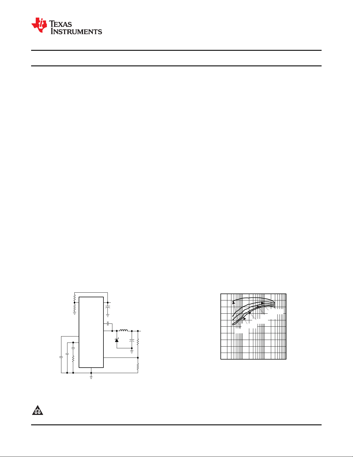
3A, 28V INPUT, STEP DOWN SWIFT™ DC/DC CONVERTER WITH Eco-mode™
1
FEATURES
2
• 3.5V to 28V Input Voltage Range
• Adjustable Output Voltage Down to 0.8V
• Integrated 80 m Ω High Side MOSFET Supports
up to 3A Continuous Output Current
• High Efficiency at Light Loads with a Pulse
Skipping Eco-mode™
• Fixed 570kHz Switching Frequency
• Typical 1 µ A Shutdown Quiescent Current
• Adjustable Slow Start Limits Inrush Currents
• Programmable UVLO Threshold
• Overvoltage Transient Protection
• Cycle by Cycle Current Limit, Frequency Fold
Back and Thermal Shutdown Protection
• Available in Easy-to-Use SOIC8 Package
• Supported by SwitcherPro™ Software Tool
(http://focus.ti.com/docs/toolsw/folders/print/s
witcherpro.html )
• For SWIFT™ Documentation, See the TI
Website at www.ti.com/swift
DESCRIPTION
The TPS54331 is a 28-V, 3-A non-synchronous buck
converter that integrates a low Rds(on) high side
MOSFET. To increase efficiency at light loads, a
pulse skipping Eco-mode™ feature is automatically
activated. Furthermore, the 1 µ A shutdown supply
current allows the device to be used in battery
powered applications. Current mode control with
internal slope compensation simplifies the external
compensation calculations and reduces component
count while allowing the use of ceramic output
capacitors. A resistor divider programs the hysterisis
of the input under-voltage lockout. An overvoltage
transient protection circuit limits voltage overshoots
during startup and transient conditions. A cycle by
cycle current limit scheme, frequency fold back and
thermal shutdown protect the device and the load in
the event of an overload condition. The TPS54331 is
available in an 8-pin SOIC package that has been
internally optimized to improve thermal performance.
APPLICATIONS
• Consumer Applications such as Set-Top
Boxes, CPE Equipment, LCD Displays,
Peripherals, and Battery Chargers
• Industrial and Car Audio Power Supplies
• 5V, 12V and 24V Distributed Power Systems
1
2 SWIFT, Eco-mode, SwitcherPro are trademarks of Texas Instruments.
PRODUCTION DATA information is current as of publication date.
Products conform to specifications per the terms of the Texas
Instruments standard warranty. Production processing does not
necessarily include testing of all parameters.
Please be aware that an important notice concerning availability, standard warranty, and use in critical applications of Texas
Instruments semiconductor products and disclaimers thereto appears at the end of this data sheet.
SIMPLIFIED SCHEMATIC EFFICIENCY
Copyright © 2008, Texas Instruments Incorporated
TPS54331
SLVS839 – JULY 2008 .......................................................................................................................................................................................................
These devices have limited built-in ESD protection. The leads should be shorted together or the device placed in conductive foam
during storage or handling to prevent electrostatic damage to the MOS gates.
ORDERING INFORMATION
T
J
– 40 ° C to 150 ° C 8 pin SOIC 570 kHz TPS54331D
(1) For the most current package and ordering information, see the Package Option Addendum at the end of this document, or see the TI
web site at www.ti.com.
(2) The D package is also available taped and reeled. Add an R suffix to the device type (i.e., TPS54331DR). See applications section of
data sheet for layout information.
ABSOLUTE MAXIMUM RATINGS
PACKAGE SWITCHING FREQUENCY PART NUMBER
(1)
(1)
www.ti.com
(2)
over operating free-air temperature range (unless otherwise noted)
VALUE UNIT
VIN – 0.3 to 30
EN – 0.3 to 5
Input Voltage V
Output Voltage PH – 0.6 to 30 V
Source Current
Sink Current COMP 100
Electrostatic Discharge (HBM) 2 kV
Electrostatic Discharge (CDM) 500 V
Operating Junction Temperature – 40 to 150 ° C
Storage Temperature – 65 to 150 ° C
(1) Stresses beyond those listed under absolute maximum ratings may cause permanent damage to the device. These are stress ratings
only, and functional operation of the device at these or any other conditions beyond those indicated under recommended operating
conditions is not implied. Exposure to absolute-maximum-rated conditions for extended periods may affect device reliabiltiy.
BOOT 38
VSENSE – 0.3 to 3
COMP – 0.3 to 3
SS – 0.3 to 3
BOOT-PH 8
PH (10 ns transient from ground to negtive peak) – 5
EN 100 µ A
BOOT 100 mA
VSENSE 10 µ A
PH 9 A
VIN 9 A
SS 200
µ A
PACKAGE DISSIPATION RATINGS
PACKAGE THERMAL IMPEDANCE JUNCTION TO PSEUDO THERMAL IMPEDANCE JUNCTION TO
SOIC8 100 ° C/W 5 ° C/W
(1) Maximum power dissipation may be limited by overcurrent protection
(2) Power rating at a specific ambient temperature TAshould be determined with a junction temperature of 150 ° C. This is the point where
distortion starts to substantially increase. Thermal management of the PCB should strive to keep the junction temperature at or below
150 ° C for best performance and long-term reliability. See power dissipation estimate in application section of this data sheet for more
information.
(3) Test board conditions:
a. 2 inches x 1.5 inches, 2 layers, thickness: 0.062 inch
b. 2-ounce copper traces located on the top and bottom of the PCB
c. 6 thermal vias located under the device package
2 Submit Documentation Feedback Copyright © 2008, Texas Instruments Incorporated
(1) (2) (3)
AMBIENT TOP
Product Folder Link(s): TPS54331
TPS54331
www.ti.com
....................................................................................................................................................................................................... SLVS839 – JULY 2008
RECOMMENDED OPERATING CONDITIONS
over operating free-air temperature range (unless otherwise noted)
MIN TYP MAX UNIT
Operating Input Voltage on (VIN pin) 3.5 28 V
Operating junction temperature, T
J
– 40 150 ° C
ELECTRICAL CHARACTERISTICS
TJ= – 40 ° C to 150 ° C, VIN = 3.5V to 28V (unless otherwise noted)
DESCRIPTION TEST CONDITIONS MIN TYP MAX UNIT
SUPPLY VOLTAGE (VIN PIN)
Internal undervoltage lockout threshold Rising and Falling 3.5 V
Shutdown supply current EN = 0V, VIN = 12V, 25 ° C 1 10 µ A
Operating – non switching supply current VSENSE = 0.85 V 110 190 µ A
ENABLE AND UVLO (EN PIN)
Enable threshold Rising and Falling 1.25 1.35 V
Input current Enable threshold – 50 mV 1 µ A
Input current Enable threshold + 50 mV 4 µ A
VOLTAGE REFERENCE
Voltage reference 0.772 0.8 0.828 V
HIGH-SIDE MOSFET
On resistance BOOT-PH = 3 V, VIN = 3.5 V 115 200 m Ω
BOOT-PH = 6 V, VIN = 12 V 80 150
ERROR AMPLIFIER
Error amplifier transconductance (gm) – 2 µ A < ICOMP < 2 µ A, V(COMP) = 1 V 92 µ mhos
Error amplifier DC gain
Error amplifier unity gain bandwidth
Error amplifier source/sink current V(COMP) = 1.0 V, 100 mV overdrive ± 7 µ A
Switch current to COMP transconductance VIN = 12 V 12 A/V
SWITCHING FREQUENCY
TPS54331 Switching Frequency VIN = 12V 400 570 740 kHz
Minimum controllable on time Measured at 90% to 90% of VIN, VIN = 12V 110 160 ns
Maximum controllable duty ratio
PULSE SKIPPING ECO-MODE™
Pulse skipping Eco-mode™ switch current threshold 160 mA
CURRENT LIMIT
Current limit threshold VIN = 12 V 3.5 5.8 A
THERMAL SHUTDOWN
Thermal Shutdown 165 ° C
SLOW START (SS PIN)
Charge current V(SS) = 0.4 V 2 µ A
SS to VSENSE matching V(SS) = 0.4 V 10 mV
(1) Specified by design
(1)
(1)
(1)
VSENSE = 0.8 V 800 V/V
5 pF capacitance from COMP to GND pins 2.7 MHz
BOOT-PH = 6 V 90 93 %
Copyright © 2008, Texas Instruments Incorporated Submit Documentation Feedback 3
Product Folder Link(s): TPS54331
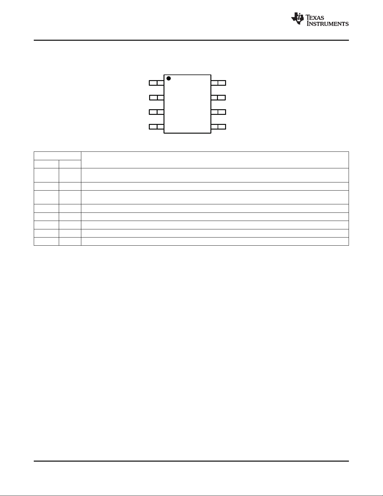
1
2
3
4
5
6
7
8
BOOT
VIN
EN
SS
PH
GND
COMP
VSENSE
TPS54331
SLVS839 – JULY 2008 .......................................................................................................................................................................................................
DEVICE INFORMATION
PIN ASSIGNMENTS
TERMINAL FUNCTIONS
TERMINAL DESCRIPTION
NAME NO.
BOOT 1 A 0.1 µ F bootstrap capacitor is required between BOOT and PH. If the voltage on this capacitor falls below the
minimum requirement, the high-side MOSFET is forced to switch off until the capacitor is refreshed.
VIN 2 Input supply voltage, 3.5 V to 28 V.
EN 3 Enable pin. Pull below 1.25V to disable. Float to enable. Programming the input undervoltage lockout with two
resistors is recommended.
SS 4 Slow start pin. An external capacitor connected to this pin sets the output rise time.
VSENSE 5 Inverting node of the gm error amplifier.
COMP 6 Error amplifier output, and input to the PWM comparator. Connect frequency compensation components to this pin.
GND 7 Ground.
PH 8 The source of the internal high-side power MOSFET.
www.ti.com
4 Submit Documentation Feedback Copyright © 2008, Texas Instruments Incorporated
Product Folder Link(s): TPS54331
Error
Amplifier
RQ
S
Boot
Charge
Boot
UVLO
Current
Sense
Oscillator
Frequency
Shift
Gate
Drive
Logic
Slope
Compensation
PWM
Latch
PWM
Comparator
ECO-MODE
MinimumClamp
™
Maximum
Clamp
Voltage
Reference
Discharge
Logic
VSENSE
COMP
PH
BOOT
VIN
GND
Thermal
Shutdown
EN
Enable
Comparator
Shutdown
Logic
Shutdown
Enable
Threshold
S
1.25V
0.8V
80mW
165C
2.1V
12 A/V
SS
Shutdown
VSENSE
1 Am
3 Am
gm=92 A/V
DCgain=800V/V
BW=2.7MHz
m
2kW
2 Am
60
65
70
75
80
85
90
95
100
105
110
-50 -25 0 25 50 75 100 125 150
T -JunctionTemperature-°C
J
Rdson-OnResistance-mW
VIN=12V
0
1
2
3
4
3 8 13 18 23 28
V -InputVoltage-V
I
Isd-ShutdownCurrent-
Am
EN=0V
T =150°C
J
T =25°C
J
T =-40°C
J
550
555
560
565
570
575
580
585
590
-50 -25 0 25 50 75 100 125 150
fsw-OscillatorFrequency-kHz
T -JunctionTemperature-°C
J
VIN=12V
TPS54331
www.ti.com
....................................................................................................................................................................................................... SLVS839 – JULY 2008
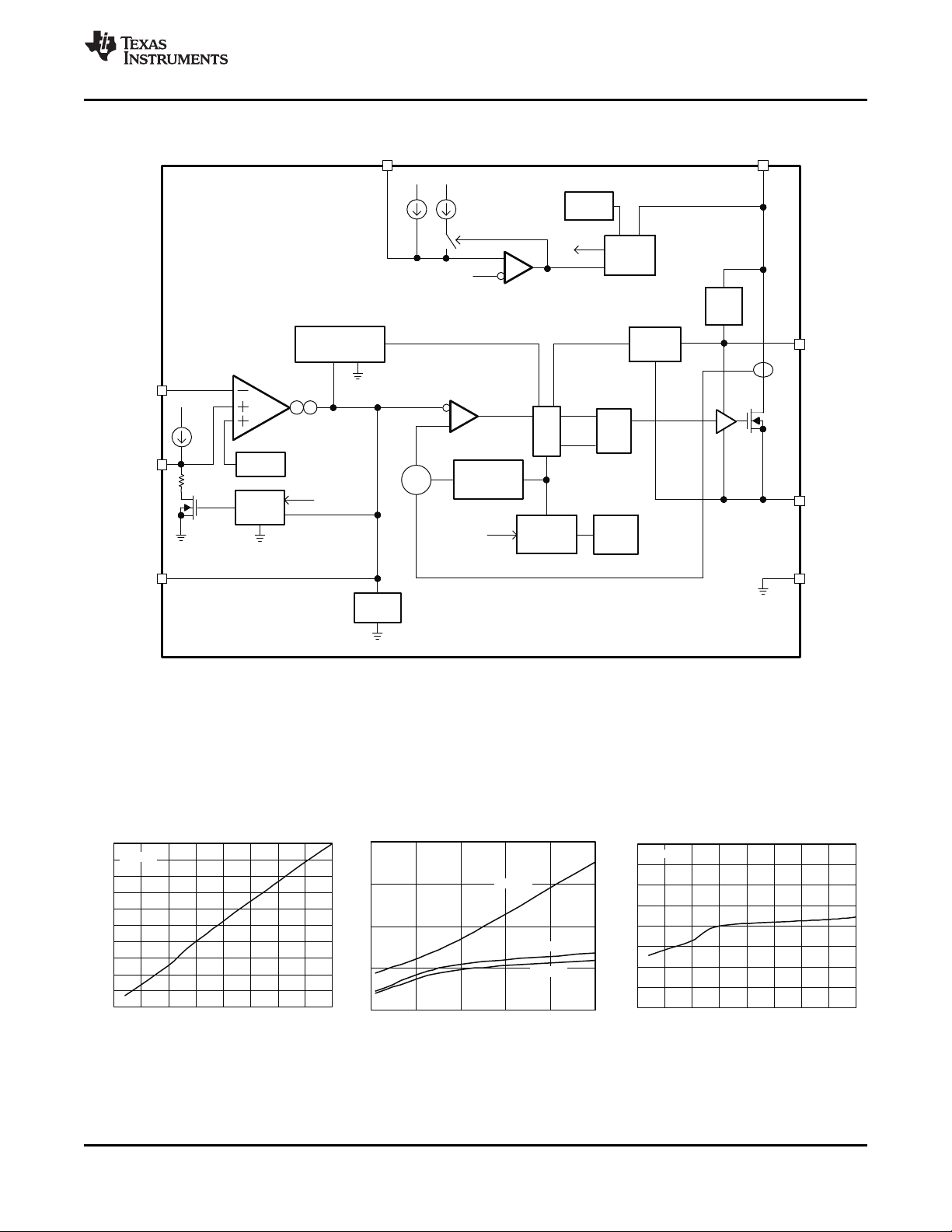
FUNCTIONAL BLOCK DIAGRAM
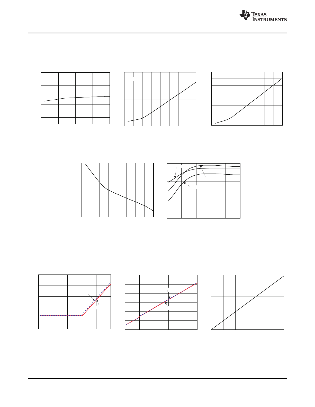
CHARACTERIZATION CURVES
ON RESISTANCE SHUTDOWN QUIESCENT CURRENT SWITCHING FREQUENCY
JUNCTION TEMPERATURE INPUT VOLTAGE JUNCTION TEMPERATURE
Copyright © 2008, Texas Instruments Incorporated Submit Documentation Feedback 5
Figure 1. Figure 2. Figure 3.
TYPICAL CHARACTERISTICS
vs vs vs
Product Folder Link(s): TPS54331
0.7760
0.7820
0.7880
0.7940
0.8000
0.8060
0.8120
0.8180
0.8240
-50 -25 0 25 50 75 100 125 150
Vref-VoltageReference-V
T -JunctionTemperature-°C
J
5.50
5.75
6
6.25
6.50
6.75
7
7.25
7.50
-50 -25 0 25 50 75 100 125 150
MinimumControllableDutyRatio-%
T -JunctionTemperature-°C
J
VIN=12V
100
110
120
130
140
-50 -25 0 25 50 75 100 125 150
Tonmin-MinimumControllableOnTime-ns
T -JunctionTemperature-°C
J
VIN=12V
1.90
2
2.10
-50 -25 0 25 50 75 100 125 150
I
-SlowStartChargeCurrent- A
SS
m
T -JunctionTemperature-°C
J
3
4
5
6
3 8 13 18 23 28
V -InputVoltage-V
I
CurrentLimitThreshold-
A
T =150°C
J
T =25°C
J
T =-40°C
J
3 8 13 18 23 28
0.5
0.75
1
1.25
1.5
1.75
V
-OutputVoltage-V
O
V -InputVolatage-V
I
I =2 A
O
I =3 A
O
3 8 13 18 23 28
0
5
10
15
20
25
30
I =3 A
O
I =2 A
O
V -OutputVoltage-V
O
V -InputVoltage-V
I
25
50
75
100
125
150
0 0.2 0.4 0.6 0.8 1 1.2
P -PowerDissipation-W
D
T -JunctionTemperature-°C
J
TPS54331
SLVS839 – JULY 2008 .......................................................................................................................................................................................................
www.ti.com
TYPICAL CHARACTERISTICS (continued)
VOLTAGE REFERENCE TIME RATIO
vs vs vs
JUNCTION TEMPERATURE JUNCTION TEMPERATURE JUNCTION TEMPERATURE
Figure 4. Figure 5. Figure 6.
SS CHARGE CURRENT CURRENT LIMIT THRESHOLD
JUNCTION TEMPERATURE INPUT VOLTAGE
MINIMUM CONTROLLABLE ON MINIMUM CONTROLLABLE DUTY
vs vs
SUPPLEMENTAL APPLICATION CURVES
TYPICAL MINIMUM OUTPUT TYPICAL MAXIMUM OUTPUT
6 Submit Documentation Feedback Copyright © 2008, Texas Instruments Incorporated
VOLTAGE VOLTAGE MAXIMUM POWER DISSIPATION
INPUT VOLTAGE INPUT VOLTAGE JUNCTION TEMPERATURE
Figure 9. Figure 10. Figure 11.
Figure 7. Figure 8.
vs vs vs
Product Folder Link(s): TPS54331

TPS54331
www.ti.com
....................................................................................................................................................................................................... SLVS839 – JULY 2008
TYPICAL CHARACTERISTICS (continued)
OVERVIEW
The TPS54331 is a 28-V, 3-A, step-down (buck) converter with an integrated high-side n-channel MOSFET. To
improve performance during line and load transients, the device implements a constant frequency, current mode
control which reduces output capacitance and simplifies external frequency compensation design. The
TPS54331 has a pre-set switching frequency of 570kHz.
The TPS54331 needs a minimum input voltage of 3.5V to operate normally. The EN pin has an internal pull-up
current source that can be used to adjust the input voltage under-voltage lockout (UVLO) with two external
resistors. In addition, the pull-up current provides a default condition when the EN pin is floating for the device to
operate. The operating current is 110 µ A typically when not switching and under no load. When the device is
disabled, the supply current is 1 µ A typically.
The integrated 80 m Ω high-side MOSFET allows for high efficiency power supply designs with continuous output
currents up to 3A.
The TPS54331 reduces the external component count by integrating the boot recharge diode. The bias voltage
for the integrated high-side MOSFET is supplied by an external capacitor on the BOOT to PH pin. The boot
capacitor voltage is monitored by an UVLO circuit and will turn the high-side MOSFET off when the voltage falls
below a preset threshold of 2.1V typically. The output voltage can be stepped down to as low as the reference
voltage.
By adding an external capacitor, the slow start time of the TPS54331 can be adjustable which enables flexible
output filter selection.
To improve the efficiency at light load conditions, the TPS54331 enters a special pulse skipping Eco-mode
when the peak inductor current drops below 160mA typically.
The frequency foldback reduces the switching frequency during startup and over current conditions to help
control the inductor current. The thermal shut down gives the additional protection under fault conditions.
TM
DETAILED DESCRIPTION
FIXED FREQUENCY PWM CONTROL
The TPS54331 uses a fixed frequency, peak current mode control. The internal switching frequency of the
TPS54331 is fixed at 570kHz.
ECO-MODE
The TPS54331 is designed to operate in pulse skipping Eco-mode
efficiency. When the peak inductor current is lower than 160 mA typically, the COMP pin voltage falls to 0.5V
typically and the device enters Eco-mode
clamped at 0.5V internally which prevents the high side integrated MOSFET from switching. The peak inductor
current must rise above 160mA for the COMP pin voltage to rise above 0.5V and exit Eco-mode
integrated current comparator catches the peak inductor current only, the average load current entering
Eco-mode
TM
TM
. When the device is in Eco-mode
TM
varies with the applications and external output filters.
TM
at light load currents to boost light load
TM
, the COMP pin voltage is
TM
. Since the
VOLTAGE REFERENCE (Vref)
The voltage reference system produces a ± 2% initial accuracy voltage reference ( ± 3.5% over temperature) by
scaling the output of a temperature stable bandgap circuit. The typical voltage reference is designed at 0.8V.
BOOTSTRAP VOLTAGE (BOOT)
The TPS54331 has an integrated boot regulator and requires a 0.1 µ F ceramic capacitor between the BOOT and
PH pin to provide the gate drive voltage for the high-side MOSFET. A ceramic capacitor with an X7R or X5R
grade dielectric is recommended because of the stable characteristics over temperature and voltage. To improve
drop out, the TPS54331 is designed to operate at 100% duty cycle as long as the BOOT to PH pin voltage is
greater than 2.1V typically.
Copyright © 2008, Texas Instruments Incorporated Submit Documentation Feedback 7
Product Folder Link(s): TPS54331
EN
1.25V
VIN
+
-
Ren1
Ren2
TPS54331
1 Am 3 Am
START STOP
V - V
Ren1 =
3 Am
EN
START EN
V
Ren2 =
V - V
+ 1 A
Ren1
m
( )
( ) ( )
( )
SS ref
SS
SS
C nF V V
T ms =
I A´m
TPS54331
SLVS839 – JULY 2008 .......................................................................................................................................................................................................
www.ti.com
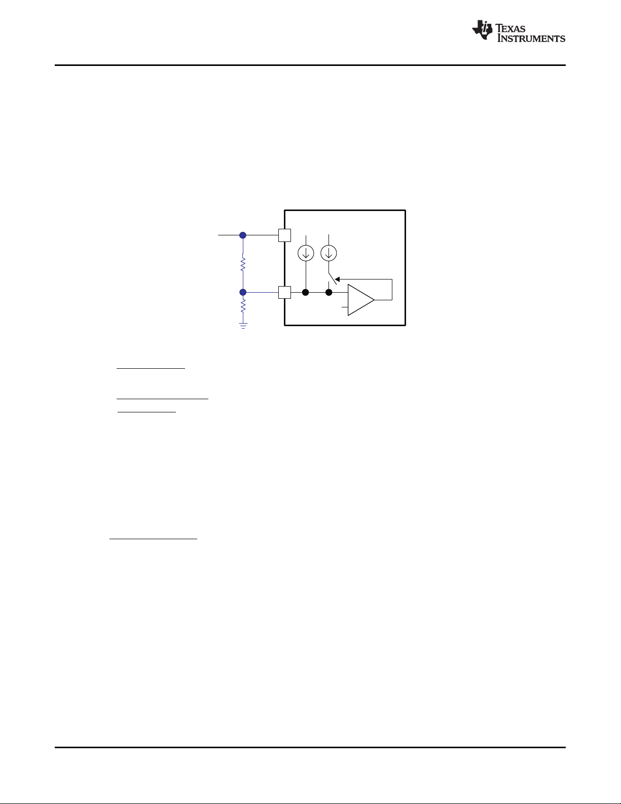
ENABLE AND ADJUSTABLE INPUT UNDER-VOLTAGE LOCKOUT (VIN UVLO)
The EN pin has an internal pull-up current source that provides the default condition of the TPS54331 operating
when the EN pin floats.
The TPS54331 is disabled when the VIN pin voltage falls below internal VIN UVLO threshold. It is recommended
to use an external VIN UVLO to add hysterisis unless VIN is greater than (VOUT + 2V). To adjust the VIN UVLO
with hysterisis, use the external circuitry connected to the EN pin as shown in Figure 12 . Once the EN pin
voltage exceeds 1.25V, an additional 3 µ A of hysteresis is added. Use Equation 1 and Equation 2 to calculate the
resistor values needed for the desired VIN UVLO threshold voltages. The V
voltage, the V
V
should always be greater than 3.5V.
STOP
is the input stop threshold voltage and the V
STOP
is the enable threshold voltage of 1.25V. The
EN
Figure 12. Adjustable Input Under-Voltage Lockout
START
is the input start threshold
PROGRAMMABLE SLOW START USING SS PIN
It is highly recommended to program the slow start time externally because no slow start time is implemented
internally. The TPS54331 effectively uses the lower voltage of the internal voltage reference or the SS pin
voltage as the power supply ’ s reference voltage fed into the error amplifier and will regulate the output
accordingly. A capacitor (Css) on the SS pin to ground implements a slow start time. The TPS54331 has an
internal pull-up current source of 2 µ A that charges the external slow start capacitor. The equation for the slow
start time (10% to 90%) is shown in Equation 3 . The Vref is 0.8V and the Iss current is 2 µ A.
The slow start time should be set between 1ms to 10ms to ensure good start-up behavior. The slow start
capacitor should be no more than 27nF.
If during normal operation, the input voltage drops below the VIN UVLO threshold, or the EN pin is pulled below
1.25V, or a thermal shutdown event occurs, the TPS54331 stops switching.
ERROR AMPLIFIER
The TPS54331 has a transconductance amplifier for the error amplifier. The error amplifier compares the
VSENSE voltage to the internal effective voltage reference presented at the input of the error amplifier. The
transconductance of the error amplifier is 92 µ A/V during normal operation. Frequency compensation
components are connected between the COMP pin and ground.
SLOPE COMPENSATION
In order to prevent the sub-harmonic oscillations when operating the device at duty cycles greater than 50%, the
TPS54331 adds a built-in slope compensation which is a compensating ramp to the switch current signal.
8 Submit Documentation Feedback Copyright © 2008, Texas Instruments Incorporated
Product Folder Link(s): TPS54331
(1)
(2)
(3)
 Loading...