

Page 1
www.ti.com
VIN
NC
NC
ENA
GND
VSENSE
BOOT
PH
TPS5430/31
VIN VOUT
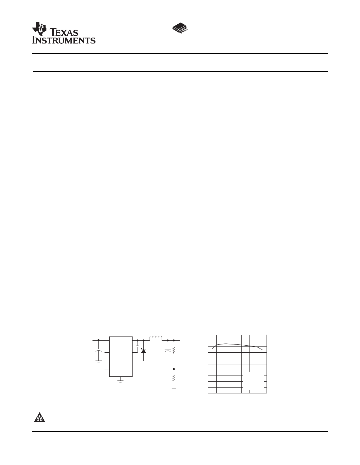
95
60
70
80
90
100
0 0.5 1 1.5 2.5 3 3.5
Efficiency − %
I OutputCurrent AO--
EfficiencyvsOutputCurrent
SimplifiedSchematic
VI=12V
V =5V
f =500kHz
T =25 C
O
s
A
o
2
50
55
65
75
85
3-A, WIDE INPUT RANGE, STEP-DOWN SWIFT™ CONVERTER
FEATURES APPLICATIONS
• Wide Input Voltage Range:
– TPS5430: 5.5 V to 36 V
– TPS5431: 5.5 V to 23 V
• Up to 3-A Continuous (4-A Peak) Output
Current
• High Efficiency up to 95% Enabled by 110-m Ω
Integrated MOSFET Switch
• Wide Output Voltage Range: Adjustable Down
to 1.22 V with 1.5% Initial Accuracy
• Internal Compensation Minimizes External
Parts Count
• Fixed 500 kHz Switching Frequency for Small
Filter Size
• Improved Line Regulation and Transient
Response by Input Voltage Feed Forward
• System Protected by Overcurrent Limiting,
Overvoltage Protection and Thermal
Shutdown
• –40 ° C to 125 ° C Operating Junction
Temperature Range
• Available in Small Thermally Enhanced 8-Pin
SOIC PowerPAD™ Package
• For SWIFT™ Documentation, Application
Notes and Design Software, See the TI
Website at www.ti.com/swift
TPS5430
TPS5431
SLVS632C – JANUARY 2006 – REVISED NOVEMBER 2006
• Consumer: Set-top Box, DVD, LCD Displays
• Industrial and Car Audio Power Supplies
• Battery Chargers, High Power LED Supply
• 12-V/24-V Distributed Power Systems
DESCRIPTION
As a member of the SWIFT™ family of DC/DC
regulators, the TPS5430/TPS5431 is a
high-output-current PWM converter that integrates a
low resistance high side N-channel MOSFET.
Included on the substrate with the listed features are
a high performance voltage error amplifier that
provides tight voltage regulation accuracy under
transient conditions; an undervoltage-lockout circuit
to prevent start-up until the input voltage reaches
5.5 V; an internally set slow-start circuit to limit inrush
currents; and a voltage feed-forward circuit to
improve the transient response. Using the ENA pin,
shutdown supply current is reduced to 18 µ A
typically. Other features include an active-high
enable, overcurrent limiting, overvoltage protection
and thermal shutdown. To reduce design complexity
and external component count, the
TPS5430/TPS5431 feedback loop is internally
compensated. The TPS5431 is intended to operate
from power rails up to 23 V. The TPS5430 regulates
a wide variety of power sources including 24-V bus.
The TPS5430/TPS5431 device is available in a
thermally enhanced, easy to use 8-pin SOIC
PowerPAD™ package. TI provides evaluation
modules and the SWIFT™ Designer software tool to
aid in quickly achieving high-performance power
supply designs to meet aggressive equipment
development cycles.
SWIFT, PowerPAD are trademarks of Texas Instruments.
PRODUCTION DATA information is current as of publication date.
Products conform to specifications per the terms of the Texas
Instruments standard warranty. Production processing does not
necessarily include testing of all parameters.
Please be aware that an important notice concerning availability, standard warranty, and use in critical applications of Texas Instruments semiconductor products and disclaimers thereto appears at the end of this data sheet.
Copyright © 2006, Texas Instruments Incorporated
Page 2
www.ti.com
TPS5430
TPS5431
SLVS632C – JANUARY 2006 – REVISED NOVEMBER 2006
These devices have limited built-in ESD protection. The leads should be shorted together or the device placed in conductive foam
during storage or handling to prevent electrostatic damage to the MOS gates.
ORDERING INFORMATION
T
J
INPUT VOLTAGE OUTPUT VOLTAGE PACKAGE
–40 ° C to 125 ° C 5.5 V to 36 V Adjustable to 1.22 V Thermally Enhanced SOIC (DDA)
–40 ° C to 125 ° C 5.5 V to 23 V Adjustable to 1.22 V Thermally Enhanced SOIC (DDA)
(1) For the most current package and ordering information, see the Package Option Addendum at the end of this document, or see the TI
web site at www.ti.com.
(2) The DDA package is also available taped and reeled. Add an R suffix to the device type (i.e., TPS5430DDAR). See applications section
of data sheet for PowerPAD™ drawing and layout information.
ABSOLUTE MAXIMUM RATINGS
over operating free-air temperature range (unless otherwise noted)
VIN –0.3 to 40
TPS5430 BOOT –0.3 to 50
V
Input voltage range
I
TPS5431 BOOT –0.3 to 35
I
O
I
lkg
T
T
Source current PH Internally Limited
Leakage current PH 10 µ A
Operating virtual junction temperature range –40 to 150 ° C
J
Storage temperature –65 to 150 ° C
stg
(1) Stresses beyond those listed under absolute maximum ratings may cause permanent damage to the device. These are stress ratings
only and functional operation of the device at these or any other conditions beyond those indicated under recommended operating
conditions is not implied. Exposure to absolute-maximum-rated conditions for extended periods may affect device reliability.
(2) All voltage values are with respect to network ground terminal.
(3) Approaching the absolute maximum rating for the VIN pin may cause the voltage on the PH pin to exceed the absolute maximum rating.
PH (steady-state) –0.6 to 40
VIN –0.3 to 25
PH (steady-state) –0.6 to 25
ENA –0.3 to 7
BOOT-PH 10
VSENSE –0.3 to 3
PH (transient < 10 ns) –1.2
(1) (2)
(1)
VALUE UNIT
PART NUMBER
(2)
(2)
TPS5430DDA
TPS5431DDA
(3)
(3)
V
DISSIPATION RATINGS
8 Pin DDA (2-layer board with solder)
8 Pin DDA (4-layer board with solder)
(1) (2)
PACKAGE
(3)
(4)
THERMAL IMPEDANCE
JUNCTION-TO-AMBIENT
33 ° C/W
26 ° C/W
(1) Maximum power dissipation may be limited by overcurrent protection.
(2) Power rating at a specific ambient temperature TAshould be determined with a junction temperature of 125 ° C. This is the point where
distortion starts to substantially increase. Thermal management of the final PCB should strive to keep the junction temperature at or
below 125 ° C for best performance and long-term reliability. See Thermal Calculations in applications section of this data sheet for more
information.
(3) Test board conditions:
a. 3 in x 3 in, 2 layers, thickness: 0.062 inch.
b. 2 oz. copper traces located on the top and bottom of the PCB.
c. 6 thermal vias in the PowerPAD area under the device package.
(4) Test board conditions:
a. 3 in x 3 in, 4 layers, thickness: 0.062 inch.
b. 2 oz. copper traces located on the top and bottom of the PCB.
c. 2 oz. copper ground planes on the 2 internal layers.
d. 6 thermal vias in the PowerPAD area under the device package.
2
Submit Documentation Feedback
Page 3
www.ti.com
TPS5430
TPS5431
SLVS632C – JANUARY 2006 – REVISED NOVEMBER 2006
RECOMMENDED OPERATING CONDITIONS
MIN NOM MAX UNIT
VIN Input voltage range V
T
Operating junction temperature –40 125 ° C
J
ELECTRICAL CHARACTERISTICS
TJ= –40 ° C to 125 ° C, VIN = 12.0 V (unless otherwise noted)
PARAMETER TEST CONDITIONS MIN TYP MAX UNIT
SUPPLY VOLTAGE (VIN PIN)
VSENSE = 2 V, Not switching,
I
Q
UNDERVOLTAGE LOCK OUT (UVLO)
VOLTAGE REFERENCE
OSCILLATOR
ENABLE (ENA PIN)
CURRENT LIMIT
THERMAL SHUTDOWN
OUTPUT MOSFET
r
DS(on)
Quiescent current
Start threshold voltage, UVLO 5.3 5.5 V
Hysteresis voltage, UVLO 330 mV
Voltage reference accuracy V
Internally set free-running frequency 400 500 600 kHz
Minimum controllable on time 150 200 ns
Maximum duty cycle 87 89 %
Start threshold voltage, ENA 1.3 V
Stop threshold voltage, ENA 0.5 V
Hysteresis voltage, ENA 450 mV
Internal slow-start time (0~100%) 6.6 8 10 ms
Current limit 4 5 6 A
Current limit hiccup time 13 16 20 ms
Thermal shutdown trip point 135 162 ° C
Thermal shutdown hysteresis 14 ° C
High-side power MOSFET switch m Ω
PH pin open
Shutdown, ENA = 0 V 18 50 µ A
TJ= 25 ° C 1.202 1.221 1.239
IO= 0 A – 3 A 1.196 1.221 1.245
VIN = 5.5 V 150
TPS5430 5.5 36
TPS5431 5.5 23
3 4.4 mA
110 230
Submit Documentation Feedback
3
Page 4
www.ti.com
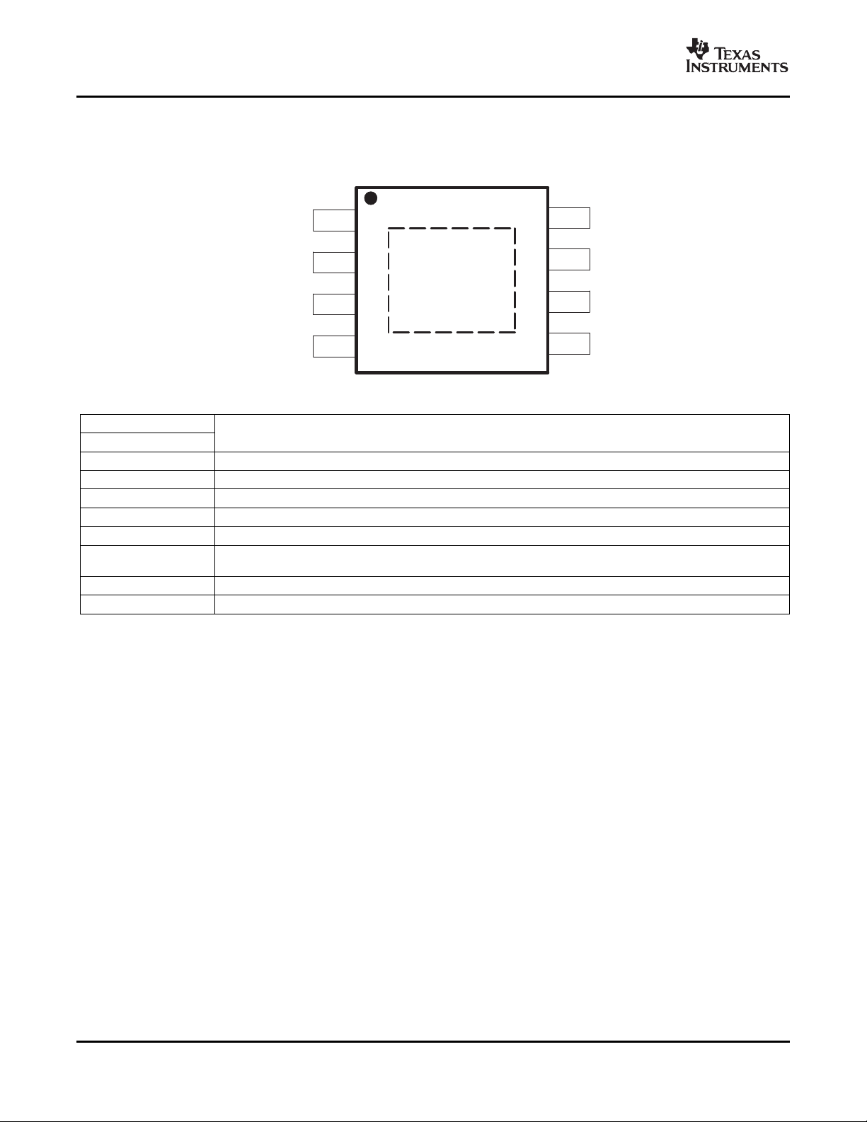
1
2
3
4
8
7
6
5
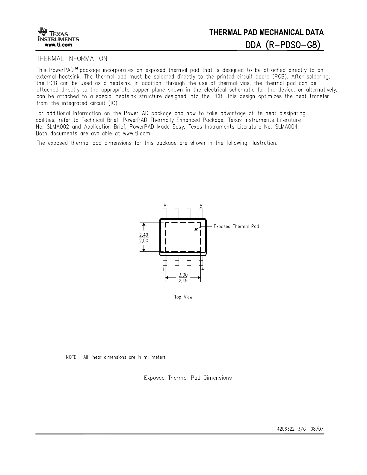
PowerPAD
(Pin9)
BOOT
NC
NC
VSENSE
PH
VIN
GND
ENA
DDAPACKAGE
(TOPVIEW)
TPS5430
TPS5431
SLVS632C – JANUARY 2006 – REVISED NOVEMBER 2006
PIN ASSIGNMENTS
TERMINAL FUNCTIONS
TERMINAL
NAME NO.
BOOT 1 Boost capacitor for the high-side FET gate driver. Connect 0.01 µ F low ESR capacitor from BOOT pin to PH pin.
NC 2, 3 Not connected internally.
VSENSE 4 Feedback voltage for the regulator. Connect to output voltage divider.
ENA 5 On/off control. Below 0.5 V, the device stops switching. Float the pin to enable.
GND 6 Ground. Connect to PowerPAD.
VIN 7
PH 8 Source of the high side power MOSFET. Connected to external inductor and diode.
PowerPAD 9 GND pin must be connected to the exposed pad for proper operation.
Input supply voltage. Bypass VIN pin to GND pin close to device package with a high quality, low ESR ceramic
capacitor.
DESCRIPTION
4
Submit Documentation Feedback
Page 5
www.ti.com
2.5
2.75
3
3.25
3.5
−50 −25 0 25 50 75 100 125
T
J
−JunctionT emperature − °C
I
Q
−QuiescentCurrent
−mA
V =12V
I
460
470
480
490
500
510
520
530
−50 −25 0 25 50 75 100 125
f − OscillatorFrequency − kHz
T − JunctionTemperature − °C
1.210
1.215
1.220
1.225
1.230
-50 -25 0 25 50 75 100 125
T -JunctionTemperature-°C
J
V -VoltageReference-V
REF
5
10
15
20
25
0 5 10 15 20 25 30 35 40
T
J
=125
°C
T
J
=27°C
TJ=
– °40 C
ENA=0V
VI−InputV oltage −V
I
SD
−ShutdownCurrent
−
Aµ
7
7.5
8
8.5
9
−50 −25 0 25 50 75 100 125
T
J
− JunctionTemperature − °C
T
S
S
− InternalSlowStartT
ime − ms
80
90
100
110
120
130
140
150
160
170
180
−50 −25 0 25 50 75 100 125
mΩ
−OnResistance
−
r
DS(on)
TJ−JunctionTemperature − °C
VI=12V
TPS5430
TPS5431
SLVS632C – JANUARY 2006 – REVISED NOVEMBER 2006
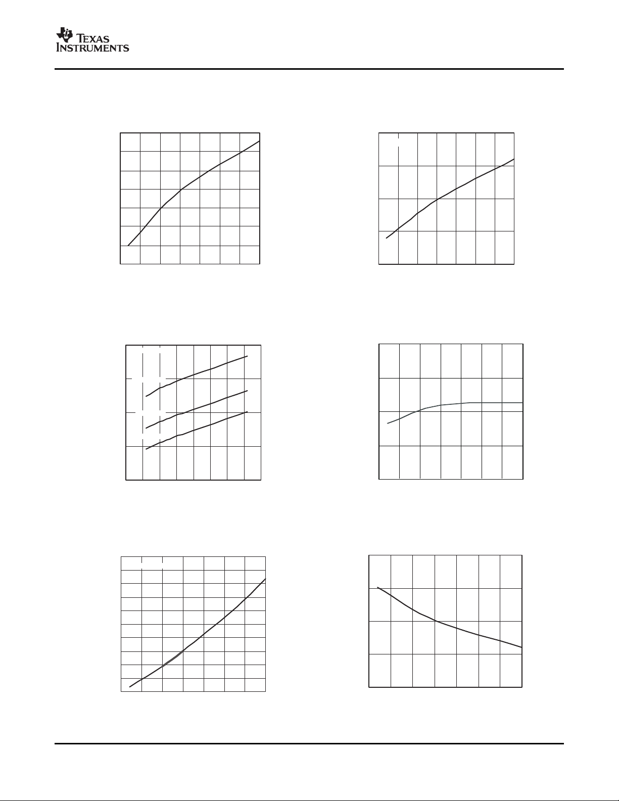
TYPICAL CHARACTERISTICS
OSCILLATOR FREQUENCY NON-SWITCHING QUIESCENT CURRENT
vs vs
JUNCTION TEMPERATURE JUNCTION TEMPERATURE
Figure 1. Figure 2.
SHUTDOWN QUIESCENT CURRENT VOLTAGE REFERENCE
vs vs
INPUT VOLTAGE JUNCTION TEMPERATURE
JUNCTION TEMPERATURE JUNCTION TEMPERATURE
Figure 3. Figure 4.
ON RESISTANCE INTERNAL SLOW START TIME
vs vs
Figure 5. Figure 6.
Submit Documentation Feedback
5
Page 6
www.ti.com
7
7.25
7.50
7.75
8
-50 -25 0 25
50
75 100 125
T -JunctionTemperature-°C
J
MinimumDutyRatio-%
120
130
140
150
160
170
180
−50 −25 0 25 50 75 100 125
T
J
− JunctionTemperature − °C
MinimumControllableOnT
ime
− ns
TPS5430
TPS5431
SLVS632C – JANUARY 2006 – REVISED NOVEMBER 2006
TYPICAL CHARACTERISTICS (continued)
MINIMUM CONTROLLABLE ON TIME MINIMUM CONTROLLABLE DUTY RATIO
vs vs
JUNCTION TEMPERATURE JUNCTION TEMPERATURE
Figure 7. Figure 8.
6
Submit Documentation Feedback
Page 7
www.ti.com
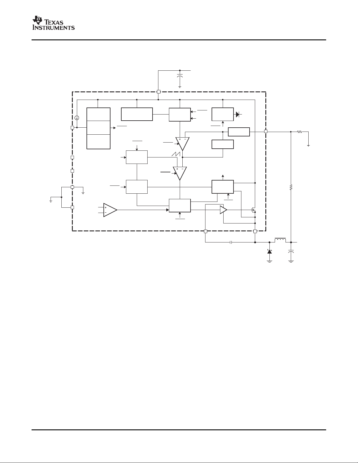
FUNCTIONAL BLOCK DIAGRAM
VIN
UVLO
ENABLE
Thermal
Protection
Reference
Overcurrent
GateDrive
Oscillator
Ramp
Generator
VREF
PH
ENA
GND
BOOT
Z1
Z2
SHDN
SHDN
SHDN
SHDN
SHDN
SHDN
SHDN
SHDN
VIN
112.5%VREF
VSENSE
OVP
HICCUP
HICCUP
SHDN
NC
FeedForward
BOOT
NC
POWERPAD
VIN
VOUT
5 µA
1.221VBandgap
SlowStart
Boot
Regulator
Error
Amplifier
Gain=25
PWM
Comparator
Protection
Gate
Driver
Control
VSENSE
TPS5430
TPS5431
SLVS632C – JANUARY 2006 – REVISED NOVEMBER 2006
APPLICATION INFORMATION
DETAILED DESCRIPTION
Oscillator Frequency
The internal free running oscillator sets the PWM switching frequency at 500 kHz. The 500 kHz switching
frequency allows less output inductance for the same output ripple requirement resulting in a smaller output
inductor.
Voltage Reference
The voltage reference system produces a precision reference signal by scaling the output of a temperature
stable bandgap circuit. The bandgap and scaling circuits are trimmed during production testing to an output of
1.221 V at room temperature.
Enable (ENA) and Internal Slow Start
The ENA pin provides electrical on/off control of the regulator. Once the ENA pin voltage exceeds the threshold
voltage, the regulator starts operation and the internal slow start begins to ramp. If the ENA pin voltage is pulled
below the threshold voltage, the regulator stops switching and the internal slow start resets. Connecting the pin
to ground or to any voltage less than 0.5 V will disable the regulator and activate the shutdown mode. The
quiescent current of the TPS5430/TPS5431 in shutdown mode is typically 18 µ A.
The ENA pin has an internal pullup current source, allowing the user to float the ENA pin. If an application
requires controlling the ENA pin, use open drain or open collector output logic to interface with the pin. To limit
the start-up inrush current, an internal slow-start circuit is used to ramp up the reference voltage from 0 V to its
final value, linearly. The internal slow start time is 8 ms typically.
Submit Documentation Feedback
7
Page 8

www.ti.com
Feed Forward Gain +
VIN
Ramp
pk*pk
TPS5430
TPS5431
SLVS632C – JANUARY 2006 – REVISED NOVEMBER 2006
APPLICATION INFORMATION (continued)
Undervoltage Lockout (UVLO)
The TPS5430/TPS5431 incorporates an undervoltage lockout circuit to keep the device disabled when VIN (the
input voltage) is below the UVLO start voltage threshold. During power up, internal circuits are held inactive and
the internal slow start is grouded until VIN exceeds the UVLO start threshold voltage. Once the UVLO start
threshold voltage is reached, the internal slow start is released and device start-up begins. The device operates
until VIN falls below the UVLO stop threshold voltage. The typical hysteresis in the UVLO comparator is 330
mV.
Boost Capacitor (BOOT)
Connect a 0.01 µ F low-ESR ceramic capacitor between the BOOT pin and PH pin. This capacitor provides the
gate drive voltage for the high-side MOSFET. X7R or X5R grade dielectrics are recommended due to their
stable values over temperature.
Output Feedback (VSENSE) and Internal Compensation
The output voltage of the regulator is set by feeding back the center point voltage of an external resistor divider
network to the VSENSE pin. In steady-state operation, the VSENSE pin voltage should be equal to the voltage
reference 1.221 V.
The TPS5430/TPS5431 implements internal compensation to simplify the regulator design. Since the
TPS5430/TPS5431 uses voltage mode control, a type 3 compensation network has been designed on chip to
provide a high crossover frequency and a high phase margin for good stability. See the Internal Compensation
Network in the applications section for more details.
Voltage Feed Forward
The internal voltage feed forward provides a constant dc power stage gain despite any variations with the input
voltage. This greatly simplifies the stability analysis and improves the transient response. Voltage feed forward
varies the peak ramp voltage inversely with the input voltage so that the modulator and power stage gain are
constant at the feed forward gain, i.e.
The typical feed forward gain of TPS5430/TPS5431 is 25.
Pulse-Width-Modulation (PWM) Control
The regulator employs a fixed frequency pulse-width-modulator (PWM) control method. First, the feedback
voltage (VSENSE pin voltage) is compared to the constant voltage reference by the high gain error amplifier and
compensation network to produce a error voltage. Then, the error voltage is compared to the ramp voltage by
the PWM comparator. In this way, the error voltage magnitude is converted to a pulse width which is the duty
cycle. Finally, the PWM output is fed into the gate drive circuit to control the on-time of the high-side MOSFET.
Overcurrent Limiting
Overcurrent limiting is implemented by sensing the drain-to-source voltage across the high-side MOSFET. The
drain to source voltage is then compared to a voltage level representing the overcurrent threshold limit. If the
drain-to-source voltage exceeds the overcurrent threshold limit, the overcurrent indicator is set true. The system
will ignore the overcurrent indicator for the leading edge blanking time at the beginning of each cycle to avoid
any turn-on noise glitches.
Once overcurrent indicator is set true, overcurrent limiting is triggered. The high-side MOSFET is turned off for
the rest of the cycle after a propagation delay. The overcurrent limiting mode is called cycle-by-cycle current
limiting.
(1)
8
Submit Documentation Feedback
Page 9

www.ti.com
TPS5430
TPS5431
SLVS632C – JANUARY 2006 – REVISED NOVEMBER 2006
APPLICATION INFORMATION (continued)
Sometimes under serious overload conditions such as short-circuit, the overcurrent runaway may still happen
when using cycle-by-cycle current limiting. A second mode of current limiting is used, i.e. hiccup mode
overcurrent limiting. During hiccup mode overcurrent limiting, the voltage reference is grounded and the
high-side MOSFET is turned off for the hiccup time. Once the hiccup time duration is complete, the regulator
restarts under control of the slow start circuit.
Overvoltage Protection
The TPS5430/TPS5431 has an overvoltage protection (OVP) circuit to minimize voltage overshoot when
recovering from output fault conditions. The OVP circuit includes an overvoltage comparator to compare the
VSENSE pin voltage and a threshold of 112.5% x VREF. Once the VSENSE pin voltage is higher than the
threshold, the high-side MOSFET will be forced off. When the VSENSE pin voltage drops lower than the
threshold, the high-side MOSFET will be enabled again.
Thermal Shutdown
The TPS5430/TPS5431 protects itself from overheating with an internal thermal shutdown circuit. If the junction
temperature exceeds the thermal shutdown trip point, the voltage reference is grounded and the high-side
MOSFET is turned off. The part is restarted under control of the slow start circuit automatically when the junction
temperature drops 14 ° C below the thermal shutdown trip point.
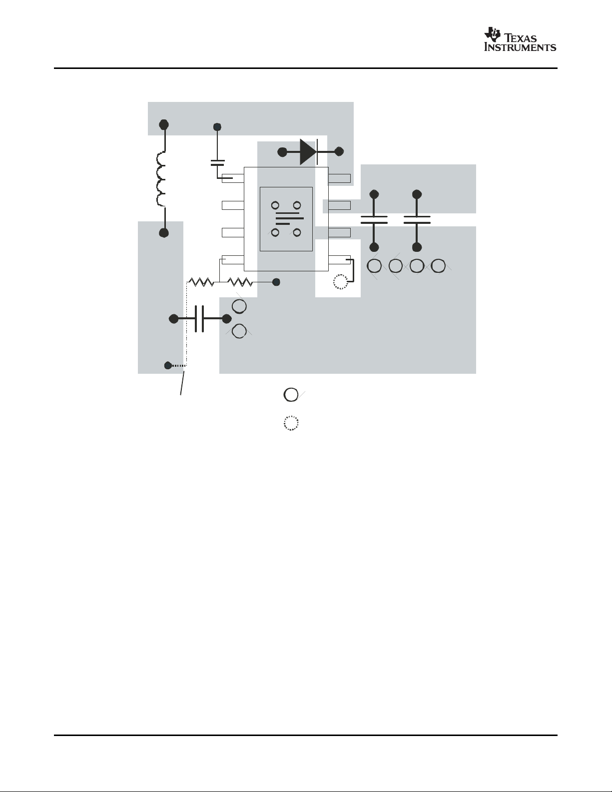
PCB Layout
Connect a low ESR ceramic bypass capacitor to the VIN pin. Care should be taken to minimize the loop area
formed by the bypass capacitor connections, the VIN pin, and the TPS5430/TPS5431 ground pin. The best way
to do this is to extend the top side ground area from under the device adjacent to the VIN trace, and place the
bypass capacitor as close as possible to the VIN pin. The minimum recommended bypass capacitance is 4.7 µ F
ceramic with a X5R or X7R dielectric.
There should be a ground area on the top layer directly underneath the IC, with an exposed area for connection
to the PowerPAD. Use vias to connect this ground area to any internal ground planes. Use additional vias at the
ground side of the input and output filter capacitors as well. The GND pin should be tied to the PCB ground by
connecting it to the ground area under the device as shown below.
The PH pin should be routed to the output inductor, catch diode and boot capacitor. Since the PH connection is
the switching node, the inductor should be located very close to the PH pin and the area of the PCB conductor
minimized to prevent excessive capacitive coupling. The catch diode should also be placed close to the device
to minimize the output current loop area. Connect the boot capacitor between the phase node and the BOOT pin
as shown. Keep the boot capacitor close to the IC and minimize the conductor trace lengths. The component
placements and connections shown work well, but other connection routings may also be effective.
Connect the output filter capacitor(s) as shown between the VOUT trace and GND. It is important to keep the
loop formed by the PH pin, Lout, Cout and GND as small as is practical.
Connect the VOUT trace to the VSENSE pin using the resistor divider network to set the output voltage. Do not
route this trace too close to the PH trace. Due to the size of the IC package and the device pin-out, the trace
may need to be routed under the output capacitor. Alternately, the routing may be done on an alternate layer if a
trace under the output capacitor is not desired.
If using the grounding scheme shown in Figure 9 , use a via connection to a different layer to route to the ENA
pin.
Submit Documentation Feedback
9
Page 10
www.ti.com
BOOT
NC
NC
VSENSE
PH
VIN
GND
ENA
VOUT
PH
Vin
TOPSIDEGROUND AREA
VIA toGroundPlane
OUTPUT
INDUCTOR
OUTPUT
FILTER
CAPACITOR
BOOT
CAPACITOR
INPUT
BYPASS
CAPACITOR
INPUT
BULK
FILTER
CATCH
DIODE
SignalVIA
Routefeedback
traceunderoutput
filtercapacitororon
otherlayer
RESISTOR
DIVIDER
TPS5430
TPS5431
SLVS632C – JANUARY 2006 – REVISED NOVEMBER 2006
APPLICATION INFORMATION (continued)
Figure 9. Design Layout
10
Submit Documentation Feedback
Page 11

www.ti.com
0.080
0.026
0.098
0.118
0.050
0.110
0.220
0.050
0.040
0.013DIA 4PL
Alldimensionsininches
+
PwPd
10.8-19.8V
L1
15 Hm
6
4
9
5
2
3
GND
VSNS
VIN
NC
NC
ENA
BOOT
PH
7
1
8
C1
10 Fm
C3
220 Fm
D1
B340A
C2
0.01 Fm
VOUT
5V
R2
3.24kW
R1
10kW
VIN
EN
U1
TPS5430DDA
APPLICATION INFORMATION (continued)
TPS5430
TPS5431
SLVS632C – JANUARY 2006 – REVISED NOVEMBER 2006
Figure 10. TPS5430 Land Pattern
Application Circuits
Figure 11 shows the schematic for a typical TPS5430 application. The TPS5430 can provide up to 3-A output
current at a nominal output voltage of 5 V. For proper thermal performance, the exposed PowerPAD™
underneath the device must be soldered down to the printed-circuit board.
Figure 11. Application Circuit, 12-V to 5.0-V
Design Procedure
The following design procedure can be used to select component values for the TPS5430. Alternately, the
SWIFT™ Designer Software may be used to generate a complete design. The SWIFT™ Designer Software
uses an iterative design procedure and accesses a comprehensive database of components when generating a
design. This section presents a simplified discussion of the design process.
Submit Documentation Feedback
11
Page 12
www.ti.com
DV
IN
+
I
OUT(MAX)
0.25
C
BULK
ƒ
sw
)
ǒ
I
OUT(MAX)
ESR
MAX
Ǔ
I
CIN
+
I
OUT(MAX)
2
TPS5430
TPS5431
SLVS632C – JANUARY 2006 – REVISED NOVEMBER 2006
APPLICATION INFORMATION (continued)
To begin the design process a few parameters must be decided upon. The designer needs to know the
following:
• Input voltage range
• Output voltage
• Input ripple voltage
• Output ripple voltage
• Output current rating
• Operating frequency
Design Parameters
For this design example, use the following as the input parameters:
DESIGN PARAMETER
Input voltage range 10.8 V to 19.8 V
Output voltage 5 V
Input ripple voltage 300 mV
Output ripple voltage 30 mV
Output current rating 3 A
Operating frequency 500 kHz
(1) As an additional constraint, the design is set up to be small size and low component height.
Switching Frequency
The switching frequency for the TPS5430 is internally set to 500 kHz. It is not possible to adjust the switching
frequency.
(1)
EXAMPLE VALUE
Input Capacitors
The TPS5430 requires an input decoupling capacitor and, depending on the application, a bulk input capacitor.
The recommended value for the decoupling capacitor, C1, is 10 µ F. A high quality ceramic type X5R or X7R is
required. For some applications, a smaller value decoupling capacitor may be used, so long as the input voltage
and current ripple ratings are not exceeded. The voltage rating must be greater than the maximum input voltage,
including ripple.
This input ripple voltage can be approximated by Equation 2 :
Where I
ESR
MAX
OUT(MAX)
is the maximum series resistance of the input capacitor.
is the maximum load current, fSWis the switching frequency, C
is the input capacitor value and
IN
The maximum RMS ripple current also needs to be checked. For worst case conditions, this can be
approximated by Equation 3 :
In this case the input ripple voltage would be 156 mV and the RMS ripple current would be 1.5 A. The maximum
voltage across the input capacitors would be VIN max plus delta VIN/2. The chosen input decoupling capacitor
is rated for 25 V and the ripple current capacity is greater than 3 A, providing ample margin. It is very important
that the maximum ratings for voltage and current are not exceeded under any circumstance.
Additionally some bulk capacitance may be needed, especially if the TPS5430 circuit is not located within about
2 inches from the input voltage source. The value for this capacitor is not critical but it also should be rated to
handle the maximum input voltage including ripple voltage and should filter the output so that input ripple voltage
is acceptable.
(2)
(3)
12
Submit Documentation Feedback
Page 13

www.ti.com
L
MIN
+
V
OUT(MAX)
ǒ
V
IN(MAX)
* V
OUT
Ǔ
V
IN(max)
K
IND
I
OUT
F
SW
I
L(RMS)
+ I
2
OUT(MAX)
)
1
12
ǒ
V
OUT
ǒ
V
IN(MAX)
* V
OUT
Ǔ
V
IN(MAX)
L
OUT
FSW 0.8
Ǔ
2
Ǹ
I
L(PK)
+ I
OUT(MAX)
)
V
OUT
ǒ
V
IN(MAX)
* V
OUT
Ǔ
1.6 V
IN(MAX)
L
OUT
F
SW
f
CO
+
f
LC
2
85 V
OUT
TPS5430
TPS5431
SLVS632C – JANUARY 2006 – REVISED NOVEMBER 2006
Output Filter Components
Two components need to be selected for the output filter, L1 and C2. Since the TPS5430 is an internally
compensated device, a limited range of filter component types and values can be supported.
Inductor Selection
To calculate the minimum value of the output inductor, use Equation 4 :
K
is a coefficient that represents the amount of inductor ripple current relative to the maximum output current.
IND
Three things need to be considered when determining the amount of ripple current in the inductor: the peak to
peak ripple current affects the output ripple voltage amplitude, the ripple current affects the peak switch current
and the amount of ripple current determines at what point the circuit becomes discontinuous. For designs using
the TPS5430, K
with the proper output capacitor, the peak switch current will be well below the current limit set point and
relatively low load currents can be sourced before discontinuous operation.
For this design example use K
highest standard value is 15 µ H, which is used in this design.
For the output filter inductor it is important that the RMS current and saturation current ratings not be exceeded.
The RMS inductor current can be found from Equation 5 :
of 0.2 to 0.3 yields good results. Low output ripple voltages can be obtained when paired
IND
= 0.2 and the minimum inductor value is calculated to be 12.5 µ H. The next
IND
(4)
and the peak inductor current can be determined with Equation 6 :
For this design, the RMS inductor current is 3.003 A, and the peak inductor current is 3.31 A. The chosen
inductor is a Sumida CDRH104R-150 15 µ H. It has a saturation current rating of 3.4 A and a RMS current rating
of 3.6 A, easily meeting these requirements. A lesser rated inductor could be used, however this device was
chosen because of its low profile component height. In general, inductor values for use with the TPS5430 are in
the range of 10 µ H to 100 µ H.
Capacitor Selection
The important design factors for the output capacitor are dc voltage rating, ripple current rating, and equivalent
series resistance (ESR). The dc voltage and ripple current ratings cannot be exceeded. The ESR is important
because along with the inductor ripple current it determines the amount of output ripple voltage. The actual value
of the output capacitor is not critical, but some practical limits do exist. Consider the relationship between the
desired closed loop crossover frequency of the design and LC corner frequency of the output filter. Due to the
design of the internal compensation, it is desirable to keep the closed loop crossover frequency in the range 3
kHz to 30 kHz as this frequency range has adequate phase boost to allow for stable operation. For this design
example, it is assumed that the intended closed loop crossover frequency will be between 2590 Hz and 24 kHz
and also below the ESR zero of the output capacitor. Under these conditions the closed loop crossover
frequency is related to the LC corner frequency by:
(5)
(6)
(7)
And the desired output capacitor value for the output filter to:
Submit Documentation Feedback
13
Page 14

www.ti.com
C
OUT
+
1
3357 L
OUT
fCO V
OUT
ESR
MAX
+
1
2p C
OUT
f
CO
V (MAX)=
PP
()
ESR xV xV -V
MAX OUT IN(MAX) OUT
N xV xL
C IN(MAX) OUT
xF
SW
I
COUT(RMS)
+
1
12
Ǹ
ȧ
ȡ
Ȣ
V
OUT
ǒ
V
IN(MAX)
* V
OUT
Ǔ
V
IN(MAX)
L
OUT
FSW N
C
ȧ
ȣ
Ȥ
R2 +
R1 1.221
V
OUT
* 1.221
TPS5430
TPS5431
SLVS632C – JANUARY 2006 – REVISED NOVEMBER 2006
For a desired crossover of 18 kHz and a 15- µ H inductor, the calculated value for the output capacitor is 220 µ F.
The capacitor type should be chosen so that the ESR zero is above the loop crossover. The maximum ESR
should be:
The maximum ESR of the output capacitor also determines the amount of output ripple as specified in the initial
design parameters. The output ripple voltage is the inductor ripple current times the ESR of the output filter.
Check that the maximum specified ESR as listed in the capacitor data sheet results in an acceptable output
ripple voltage:
Where:
∆ V
is the desired peak-to-peak output ripple.
PP
N
is the number of parallel output capacitors.
C
F
is the switching frequency.
SW
For this design example, a single 220- µ F output capacitor is chosen for C3. The calculated RMS ripple current is
143 mA and the maximum ESR required is 40 m Ω . A capacitor that meets these requirements is a Sanyo
Poscap 10TPB220M, rated at 10 V with a maximum ESR of 40 m Ω and a ripple current rating of 3 A. An
additional small 0.1- µ F ceramic bypass capacitor may also used, but is not included in this design.
The minimum ESR of the output capacitor should also be considered. For good phase margin, the ESR zero
when the ESR is at a minimum should not be too far above the internal compensation poles at 24 kHz and 54
kHz.
The selected output capacitor must also be rated for a voltage greater than the desired output voltage plus one
half the ripple voltage. Any derating amount must also be included. The maximum RMS ripple current in the
output capacitor is given by Equation 11 :
(8)
(9)
(10)
Where:
N
is the number of output capacitors in parallel.
C
F
is the switching frequency.
SW
Other capacitor types can be used with the TPS5430, depending on the needs of the application.
Output Voltage Setpoint
The output voltage of the TPS5430 is set by a resistor divider (R1 and R2) from the output to the VSENSE pin.
Calculate the R2 resistor value for the output voltage of 5 V using Equation 12 :
For any TPS5430 design, start with an R1 value of 10 k Ω . R2 is then 3.24 k Ω .
Boot Capacitor
The boot capacitor should be 0.01 µ F.
14
Submit Documentation Feedback
(11)
(12)
Page 15

www.ti.com
+
10-35V
VIN
C1
4.7 Fm
C4
4.7 Fm
ENA
VIN
ENA
NC
NC
GND
PwPd
BOOT
PH
VSNS
U1
TPS5430DDA
C2
0.01 Fm
L1
22 Hm
D1
B340A
C3
220 Fm
R2
3.24kW
5V
VOUT
R1
10kW
C3=SanyoPOSCAP 10TP220M
+
9-21V
VIN
C1
ENA
VIN
ENA
NC
NC
GND
PwPd
BOOT
PH
VSNS
U1
TPS5431DDA
C2
0.01 Fm
L1
18 Hm
D1
B340A
C3
220 Fm
R2
3.24kW
5V
VOUT
R1
10kW
C3=SanyoPOSCAP 10TP220M
TPS5430
TPS5431
SLVS632C – JANUARY 2006 – REVISED NOVEMBER 2006
Catch Diode
The TPS5430 is designed to operate using an external catch diode between PH and GND. The selected diode
must meet the absolute maximum ratings for the application: Reverse voltage must be higher than the maximum
voltage at the PH pin, which is VINMAX + 0.5 V. Peak current must be greater than IOUTMAX plus on half the
peak to peak inductor current. Forward voltage drop should be small for higher efficiencies. It is important to
note that the catch diode conduction time is typically longer than the high-side FET on time, so attention paid to
diode parameters can make a marked improvement in overall efficiency. Additionally, check that the device
chosen is capable of dissipating the power losses. For this design, a Diodes, Inc. B340A is chosen, with a
reverse voltage of 40 V, forward current of 3 A, and a forward voltage drop of 0.5 V.
Additional Circuits
Figure 12 and Figure 13 show application circuits using wide input voltage ranges. The design parameters are
similar to those given for the design example, with a larger value output inductor and a lower closed loop
crossover frequency.
Figure 12. 10–35 V Input to 5 V Output Application Circuit
Figure 13. 9–21 V Input to 5 V Output Application Circuit
Circuit Using Ceramic Output Filter Capacitors
Figure 14 shows an application circuit using all ceramic capacitors for the input and output filters which
generates a 3.3-V output from a 10-V to 24-V input. The design procedure is similar to those given for the
design example, except for the selection of the output filter capacitor values and the design of the additional
compensation components required to stabilize the circuit.
Submit Documentation Feedback
15
Page 16

www.ti.com
VIN10 24V-
C1
4.7 Fm
L1
15 Hm
R1
10kW
R2
5.9kW
R3
549 W
C6
1500pF
U1
TPS5430DDA
VIN
GND
VSNS
PH
BOOT
PwPd
EN
3.3V
VOUT
C2
0.01 Fm
D1
MRBS340
C3
100 Fm
C7
0.1 Fm
C4
150pF
VIN
7
1
2
4
5
8
3
6
9
ENA
NC
NC
C (MIN)
O
³
1
2
(2 x7000)xLp
O
F =
LC
1
2 Lp
O O
xC (EFF)Ö
TPS5430
TPS5431
SLVS632C – JANUARY 2006 – REVISED NOVEMBER 2006
Figure 14. Ceramic Output Filter Capacitors Circuit
Output Filter Component Selection
Using Equation 11 , the minimum inductor value is 12 µ H. A value of 15 µ H is chosen for this design.
When using ceramic output filer capacitors, the recommended LC resonant frequency should be no more than
7 kHz. Since the output inductor is already selected at 15 µ H, this limits the minimum output capacitor value to:
The minimum capacitor value is calculated to be 34 µ F. For this circuit a larger value of capacitor yields better
transient response. A single 100- µ F output capacitor is used for C3. It is important to note that the actual
capacitance of ceramic capacitors decreases with applied voltage. In this example, the output voltage is set to
3.3 V, minimizing this effect.
External Compensation Network
When using ceramic output capacitors, additional circuitry is required to stabilize the closed loop system. For
this circuit, the external components are R3, C4, C6, and C7. To determine the value of these components, first
calculate the LC resonant frequency of the output filter:
For this example the effective resonant frequency is calculated as 4109 Hz
The network composed of R1, R2, R3, C5, C6, and C7 has two poles and two zeros that are used to tailor the
overall response of the feedback network to accommodate the use of the ceramic output capacitors. The pole
and zero locations are given by the following equations:
16
Submit Documentation Feedback
(13)
(14)
Page 17

www.ti.com
Fp1=500000x
V
O
F
LC
Fz1=0.7xF
LC
Fz2=2.5xF
LC
C7=
1
2 xFp1x(R1||R2)p
R3=
1
2 xFz1xC7p
C6=
1
2 xFz2xR1p
V
OUTMAX
+ 0.87 ǒǒV
INMIN
* I
OMAX
0.230Ǔ) V
D
Ǔ
*
ǒ
I
OMAX
R
L
Ǔ
* V
D
V
OUTMIN
+ 0.12 ǒǒV
INMAX
* I
OMIN
0.110Ǔ) V
D
Ǔ
*
ǒ
I
OMIN
R
L
Ǔ
* V
D
TPS5430
TPS5431
SLVS632C – JANUARY 2006 – REVISED NOVEMBER 2006
The final pole is located at a frequency too high to be of concern. The second zero, Fz2 as defined by
Equation 17 uses 2.5 for the frequency multiplier. In some cases this may need to be slightly higher or lower.
Values in the range of 2.3 to 2.7 work well. The values for R1 and R2 are fixed by the 3.3-V output voltage as
calculated usingEquation 12 . For this design R1 = 10 k Ω and R2 = 5.90 k Ω . With Fp1 = 401 Hz, Fz1 = 2876 Hz
and Fz2 = 10.3 kHz, the values of R3, C6 and C7 are determined using Equation 18 , Equation 19 , and
Equation 20 :
For this design, using the closest standard values, C7 is 0.1 µ F, R3 is 549 Ω , and C6 is 1500 pF. C4 is added to
improve load regulation performance. It is effectively in parallel with C6 in the location of the second pole
frequency, so it should be small in relationship to C6. C4 should be less the 1/10 the value of C6. For this
example, 150 pF works well.
For additional information on external compensation of the TPS5430, TPS5431 or other wide voltage range
SWIFT devices, see SLVA237 Using TPS5410/20/30/31 With Aluminum/Ceramic Output Capacitors
(15)
(16)
(17)
(18)
(19)
(20)
ADVANCED INFORMATION
Output Voltage Limitations
Due to the internal design of the TPS5430, there are both upper and lower output voltage limits for any given
input voltage. The upper limit of the output voltage set point is constrained by the maximum duty cycle of 87%
and is given by:
Where
V
= minimum input voltage
INMIN
I
= maximum load current
OMAX
V
= catch diode forward voltage.
D
RL= output inductor series resistance.
This equation assumes maximum on resistance for the internal high side FET.
The lower limit is constrained by the minimum controllable on time which may be as high as 200 ns. The
approximate minimum output voltage for a given input voltage and minimum load current is given by:
Where
V
I
V
RL= output inductor series resistance.
This equation assumes nominal on resistance for the high side FET and accounts for worst case variation of
operating frequency set point. Any design operating near the operational limits of the device should be
carefully checked to assure proper functionality.
= maximum input voltage
INMAX
= minimum load current
OMIN
= catch diode forward voltage.
D
(21)
(22)
Submit Documentation Feedback
17
Page 18

www.ti.com
H(s) +
ǒ
1 )
s
2p Fz1
Ǔ ǒ
1 )
s
2p Fz2
Ǔ
ǒ
s
2p Fp0
Ǔ ǒ
1 )
s
2p Fp1
Ǔ ǒ
1 )
s
2p Fp2
Ǔ ǒ
1 )
s
2p Fp3
Ǔ
TPS5430
TPS5431
SLVS632C – JANUARY 2006 – REVISED NOVEMBER 2006
Internal Compensation Network
The design equations given in the example circuit can be used to generate circuits using the
TPS5430/TPS5431. These designs are based on certain assumptions and will tend to always select output
capacitors within a limited range of ESR values. If a different capacitor type is desired, it may be possible to fit
one to the internal compensation of the TPS5430/TPS5431. Equation 23 gives the nominal frequency response
of the internal voltage-mode type III compensation network:
Where
Fp0 = 2165 Hz, Fz1 = 2170 Hz, Fz2 = 2590 Hz
Fp1 = 24 kHz, Fp2 = 54 kHz, Fp3 = 440 kHz
Fp3 represents the non-ideal parasitics effect.
Using this information along with the desired output voltage, feed forward gain and output filter characteristics,
the closed loop transfer function can be derived.
Thermal Calculations
The following formulas show how to estimate the device power dissipation under continuous conduction mode
operations. They should not be used if the device is working at light loads in the discontinuous conduction mode.
Conduction Loss: Pcon = I
Switching Loss: Psw = V
Quiescent Current Loss: Pq = V
Total Loss: Ptot = Pcon + Psw + Pq
Given TA=> Estimated Junction Temperature: TJ= TA+ Rth x Ptot
Given T
= 125 ° C => Estimated Maximum Ambient Temperature: T
JMAX
2
x Rds(on) x V
OUT
x I
IN
x 0.01
OUT
x 0.01
IN
/V
OUT
IN
= T
AMAX
– Rth x Ptot
JMAX
(23)
18
Submit Documentation Feedback
Page 19

www.ti.com
-0.3
-0.2
-0.1
0
0.1
0.2
0.3
0 0.5 1 1.5
2
2.5 3
I -OutputCurrent- A
O
OutputRegulation-%
75
80
85
90
95
100
0 0.5 1 1.5 2 2.5 3 3.5
I -OutputCurrent- A
O
Efficiency-%
V =15V
I
V =10.8V
I
V =12V
I
V =18V
I
V =19.8V
I
t-Time-500ns/Div
PH=5V/Div
V =100mV/Div(ACCoupled)
IN
-0.1
-0.08
-0.06
-0.04
-0.02
0
0.02
0.04
0.06
0.08
0.1
10.8 13.8 16.8 19.8
V -InputVoltage-V
I
InputRegulation-%
I =0 A
O
I =3 A
O
I =1.5 A
O
TPS5430
TPS5431
SLVS632C – JANUARY 2006 – REVISED NOVEMBER 2006
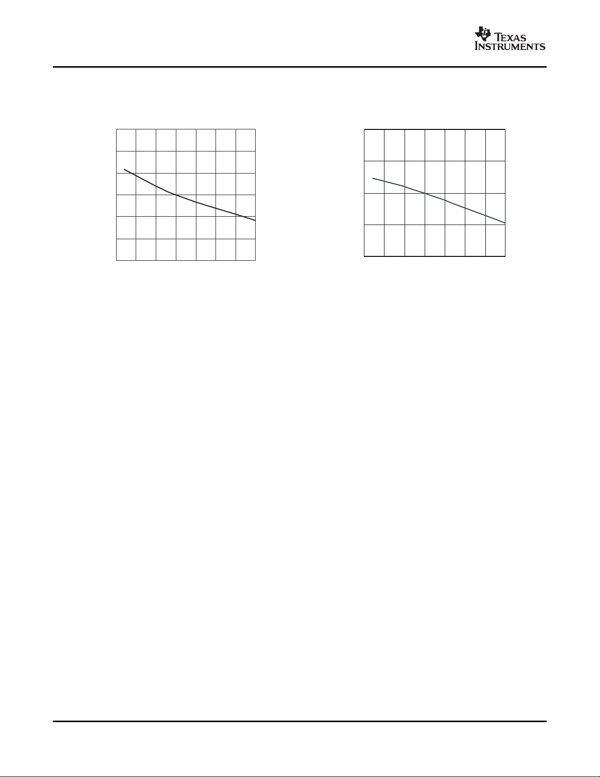
PERFORMANCE GRAPHS
The performance graphs (Figure 15 through Figure 21 ) are applicable to the circuit in Figure 11 . Ta = 25 ° C.
unless otherwise specified.
Figure 15. Efficiency vs. Output Current Figure 16. Output Regulation % vs. Output Current
Figure 17. Input Regulation % vs. Input Voltage Figure 18. Input Voltage Ripple and PH Node, Io = 3 A.
Submit Documentation Feedback
19
Page 20

www.ti.com
t-Time=500ns/Div
PH=5V/Div
V =20mV/Div(ACCoupled)
OUT
t-Time=200 μs/Div
I =1 A /Div
OUT
V =50mV/Div(ACCoupled)
OUT
t-Time=2ms/Div
V =2V/Div
OUT
V =5V/Div
IN
TPS5430
TPS5431
SLVS632C – JANUARY 2006 – REVISED NOVEMBER 2006
Figure 19. Output Voltage Ripple and PH Node, Io = 3 A Figure 20. Transient Response, Io Step 0.75 to 2.25 A.
20
Figure 21. Startup Waveform, Vin and Vout.
Submit Documentation Feedback
Page 21

PACKAGE OPTION ADDENDUM
www.ti.com
31-Oct-2008
PACKAGING INFORMATION
Orderable Device Status
TPS5430DDA ACTIVE SO
(1)
Package
Type
Power
Package
Drawing
Pins Package
Qty
Eco Plan
DDA 8 100 Green (RoHS &
no Sb/Br)
PAD
TPS5430DDAG4 ACTIVE SO
Power
DDA 8 100 Green (RoHS &
no Sb/Br)
PAD
TPS5430DDAR ACTIVE SO
Power
DDA 8 2500 Green (RoHS &
no Sb/Br)
PAD
TPS5430DDARG4 ACTIVE SO
Power
DDA 8 2500 Green (RoHS &
no Sb/Br)
PAD
TPS5431DDA ACTIVE SO
Power
DDA 8 100 Green (RoHS &
no Sb/Br)
PAD
TPS5431DDAG4 ACTIVE SO
Power
DDA 8 100 Green (RoHS &
no Sb/Br)
PAD
TPS5431DDAR ACTIVE SO
Power
DDA 8 2500 Green (RoHS &
no Sb/Br)
PAD
TPS5431DDARG4 ACTIVE SO
Power
DDA 8 2500 Green (RoHS &
no Sb/Br)
PAD
(1)
The marketing status values are defined as follows:
ACTIVE: Product device recommended for new designs.
LIFEBUY: TI has announced that the device will be discontinued, and a lifetime-buy period is in effect.
NRND: Not recommended for new designs. Device is in production to support existing customers, but TI does not recommend using this part in
a new design.
PREVIEW: Device has been announced but is not in production. Samples may or may not be available.
OBSOLETE: TI has discontinued the production of the device.
(2)
Lead/Ball Finish MSL Peak Temp
CU NIPDAU Level-1-260C-UNLIM
CU NIPDAU Level-1-260C-UNLIM
CU NIPDAU Level-1-260C-UNLIM
CU NIPDAU Level-1-260C-UNLIM
CU NIPDAU Level-1-260C-UNLIM
CU NIPDAU Level-1-260C-UNLIM
CU NIPDAU Level-1-260C-UNLIM
CU NIPDAU Level-1-260C-UNLIM
(3)
(2)
Eco Plan - The planned eco-friendly classification: Pb-Free (RoHS), Pb-Free (RoHS Exempt), or Green (RoHS & no Sb/Br) - please check
http://www.ti.com/productcontent for the latest availability information and additional product content details.
TBD: The Pb-Free/Green conversion plan has not been defined.
Pb-Free (RoHS): TI's terms "Lead-Free" or "Pb-Free" mean semiconductor products that are compatible with the current RoHS requirements
for all 6 substances, including the requirement that lead not exceed 0.1% by weight in homogeneous materials. Where designed to be soldered
at high temperatures, TI Pb-Free products are suitable for use in specified lead-free processes.
Pb-Free (RoHS Exempt): This component has a RoHS exemption for either 1) lead-based flip-chip solder bumps used between the die and
package, or 2) lead-based die adhesive used between the die and leadframe. The component is otherwise considered Pb-Free (RoHS
compatible) as defined above.
Green (RoHS & no Sb/Br): TI defines "Green" to mean Pb-Free (RoHS compatible), and free of Bromine (Br) and Antimony (Sb) based flame
retardants (Br or Sb do not exceed 0.1% by weight in homogeneous material)
(3)
MSL, Peak Temp. -- The Moisture Sensitivity Level rating according to the JEDEC industry standard classifications, and peak solder
temperature.
Important Information and Disclaimer:The information provided on this page represents TI's knowledge and belief as of the date that it is
provided. TI bases its knowledge and belief on information provided by third parties, and makes no representation or warranty as to the
accuracy of such information. Efforts are underway to better integrate information from third parties. TI has taken and continues to take
reasonable steps to provide representative and accurate information but may not have conducted destructive testing or chemical analysis on
incoming materials and chemicals. TI and TI suppliers consider certain information to be proprietary, and thus CAS numbers and other limited
information may not be available for release.
Addendum-Page 1
Page 22

PACKAGE OPTION ADDENDUM
www.ti.com
In no event shall TI's liability arising out of such information exceed the total purchase price of the TI part(s) at issue in this document sold by TI
to Customer on an annual basis.
OTHER QUALIFIED VERSIONS OF TPS5430 :
Automotive: TPS5430-Q1
•
NOTE: Qualified Version Definitions:
Automotive - Q100 devices qualified for high-reliability automotive applications targeting zero defects
•
31-Oct-2008
Addendum-Page 2
Page 23

PACKAGE MATERIALS INFORMATION
www.ti.com
TAPE AND REEL INFORMATION
31-Oct-2008
*All dimensions are nominal
Device Package
TPS5430DDAR SO
TPS5431DDAR SO
Type
Power
PAD
Power
PAD
Package
Drawing
Pins SPQ Reel
Diameter
(mm)
DDA 8 2500 330.0 12.4 6.4 5.2 2.1 8.0 12.0 Q1
DDA 8 2500 330.0 12.4 6.4 5.2 2.1 8.0 12.0 Q1
Reel
Width
W1 (mm)
A0 (mm) B0 (mm) K0 (mm) P1
(mm)W(mm)
Pin1
Quadrant
Pack Materials-Page 1
Page 24
PACKAGE MATERIALS INFORMATION
www.ti.com
31-Oct-2008
*All dimensions are nominal
Device Package Type Package Drawing Pins SPQ Length (mm) Width (mm) Height (mm)
TPS5430DDAR SO PowerPAD DDA 8 2500 346.0 346.0 29.0
TPS5431DDAR SO PowerPAD DDA 8 2500 346.0 346.0 29.0
Pack Materials-Page 2
Page 25

Page 26
Page 27

IMPORTANT NOTICE
Texas Instruments Incorporated and its subsidiaries (TI) reserve the right to make corrections, modifications, enhancements, improvements,
and other changes to its products and services at any time and to discontinue any product or service without notice. Customers should
obtain the latest relevant information before placing orders and should verify that such information is current and complete. All products are
sold subject to TI’s terms and conditions of sale supplied at the time of order acknowledgment.
TI warrants performance of its hardware products to the specifications applicable at the time of sale in accordance with TI’s standard
warranty. Testing and other quality control techniques are used to the extent TI deems necessary to support this warranty. Except where
mandated by government requirements, testing of all parameters of each product is not necessarily performed.
TI assumes no liability for applications assistance or customer product design. Customers are responsible for their products and
applications using TI components. To minimize the risks associated with customer products and applications, customers should provide
adequate design and operating safeguards.
TI does not warrant or represent that any license, either express or implied, is granted under any TI patent right, copyright, mask work right,
or other TI intellectual property right relating to any combination, machine, or process in which TI products or services are used. Information
published by TI regarding third-party products or services does not constitute a license from TI to use such products or services or a
warranty or endorsement thereof. Use of such information may require a license from a third party under the patents or other intellectual
property of the third party, or a license from TI under the patents or other intellectual property of TI.
Reproduction of TI information in TI data books or data sheets is permissible only if reproduction is without alteration and is accompanied
by all associated warranties, conditions, limitations, and notices. Reproduction of this information with alteration is an unfair and deceptive
business practice. TI is not responsible or liable for such altered documentation. Information of third parties may be subject to additional
restrictions.
Resale of TI products or services with statements different from or beyond the parameters stated by TI for that product or service voids all
express and any implied warranties for the associated TI product or service and is an unfair and deceptive business practice. TI is not
responsible or liable for any such statements.
TI products are not authorized for use in safety-critical applications (such as life support) where a failure of the TI product would reasonably
be expected to cause severe personal injury or death, unless officers of the parties have executed an agreement specifically governing
such use. Buyers represent that they have all necessary expertise in the safety and regulatory ramifications of their applications, and
acknowledge and agree that they are solely responsible for all legal, regulatory and safety-related requirements concerning their products
and any use of TI products in such safety-critical applications, notwithstanding any applications-related information or support that may be
provided by TI. Further, Buyers must fully indemnify TI and its representatives against any damages arising out of the use of TI products in
such safety-critical applications.
TI products are neither designed nor intended for use in military/aerospace applications or environments unless the TI products are
specifically designated by TI as military-grade or "enhanced plastic." Only products designated by TI as military-grade meet military
specifications. Buyers acknowledge and agree that any such use of TI products which TI has not designated as military-grade is solely at
the Buyer's risk, and that they are solely responsible for compliance with all legal and regulatory requirements in connection with such use.
TI products are neither designed nor intended for use in automotive applications or environments unless the specific TI products are
designated by TI as compliant with ISO/TS 16949 requirements. Buyers acknowledge and agree that, if they use any non-designated
products in automotive applications, TI will not be responsible for any failure to meet such requirements.
Following are URLs where you can obtain information on other Texas Instruments products and application solutions:
Products Applications
Amplifiers amplifier.ti.com Audio www.ti.com/audio
Data Converters dataconverter.ti.com Automotive www.ti.com/automotive
DSP dsp.ti.com Broadband www.ti.com/broadband
Clocks and Timers www.ti.com/clocks Digital Control www.ti.com/digitalcontrol
Interface interface.ti.com Medical www.ti.com/medical
Logic logic.ti.com Military www.ti.com/military
Power Mgmt power.ti.com Optical Networking www.ti.com/opticalnetwork
Microcontrollers microcontroller.ti.com Security www.ti.com/security
RFID www.ti-rfid.com Telephony www.ti.com/telephony
RF/IF and ZigBee® Solutions www.ti.com/lprf Video & Imaging www.ti.com/video
Mailing Address: Texas Instruments, Post Office Box 655303, Dallas, Texas 75265
Copyright © 2008, Texas Instruments Incorporated
Wireless www.ti.com/wireless
 Loading...