

Texas Instruments TPS3831A09DQNR, TPS3831E16DQNR, TPS3831G12DQNR, TPS3831G18DQNR, TPS3831G33DQNR Schematic [ru]
...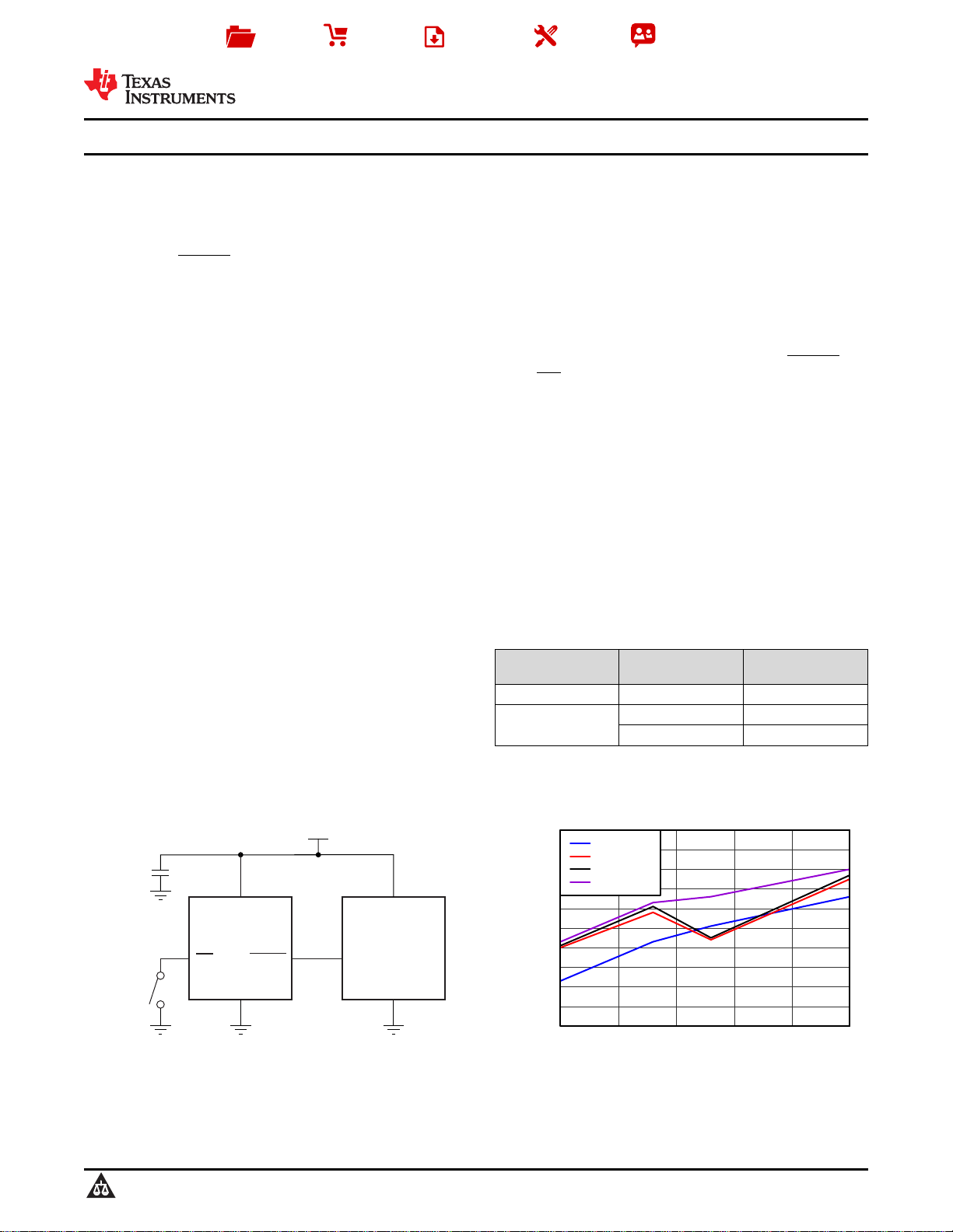
100
110
120
130
140
150
160
170
180
190
200
−40 −15 10 35 60 85
Temperature (°C)
Supply Current (nA)
VDD = 1.2 V
VDD = 3.3 V
VDD = 5.0 V
VDD = 6.5 V
G001
VDD
RESET
GND
TPS383xK33
RST
Microprocessor
3.3 V
C
0.1 F1m
MR
TPS3831
Only
Product
Folder
Sample &
Buy
Technical
Documents
Tools &
Software
Support &
Community
TPS3831, TPS3839
SBVS193D –JUNE 2012–REVISED JULY 2015
TPS383x 150-nA, Ultralow Power, Supply Voltage Monitor
1 Features 3 Description
1
• Ultralow Supply Current: 150 nA (Typical)
• Operating Supply Voltage: 0.9 V to 6.5 V
• Valid Reset for VDD> 0.6 V
• Push-Pull RESET Output
• Factory-Trimmed Reset Threshold Voltages
• Temperature Range: –40°C to 85°C
• Packages: 1-mm × 1-mm X2SON or 3-Pin SOT23
2 Applications
• Portable and Battery-Powered Equipment
• Metering
• Industrial Equipment
• Cell Phones specified to have the correct output logic state for
• Glucose Monitors
• Tablets
• Wearables
The TPS3831 and TPS3839 devices (both referred to
as TPS383x) are ultralow current (150 nA, typical),
voltage supervisory circuits that monitor a single
voltage. Both devices initiate an active-low reset
signal whenever the VDDsupply voltage drops below
the factory-trimmed reset threshold voltage. The reset
output remains low for 200 ms (typical) after the V
DD
voltage rises above the threshold voltage and
hysteresis. These devices are designed to ignore fast
transients on the VDD pin. The TPS3831 device
includes a manual reset input that forces RESET low
when MR is low.
The ultralow current consumption of 150 nA makes
these voltage supervisors ideal for use in low-power
and portable applications. The TPS383x devices are
supply voltages down to 0.6 V.
The TPS383x devices feature precision factory-
trimmed threshold voltages and extremely low-power
operation. The TPS3831 device is available in a 4pin, 1-mm × 1-mm (DQN) X2SON package. The
TPS3839 device is available in a 3-pin SOT23 (DBZ)
package or a 4-pin, 1-mm × 1-mm (DQN) X2SON
package.
Device Information
PART NUMBER PACKAGE
TPS3831 X2SON (4) 1.00 mm x 1.00 mm
TPS3839
(1) For all available packages, see the orderable addendum at
the end of the data sheet.
SOT-23 (3) 2.92 mm x 2.37 mm
X2SON (4) 1.00 mm x 1.00 mm
(1)
PACKAGE SIZE
Typical Application Circuit Supply Current vs Temperature
1
An IMPORTANT NOTICE at the end of this data sheet addresses availability, warranty, changes, use in safety-critical applications,
intellectual property matters and other important disclaimers. PRODUCTION DATA.
(NOM)

TPS3831, TPS3839
SBVS193D –JUNE 2012–REVISED JULY 2015
www.ti.com
Table of Contents
1 Features.................................................................. 1
2 Applications ........................................................... 1
3 Description ............................................................. 1
4 Revision History..................................................... 2
5 Device Options....................................................... 4
6 Pin Configuration and Functions......................... 5
7 Specifications......................................................... 6
7.1 Absolute Maximum Ratings...................................... 6
7.2 ESD Ratings.............................................................. 6
7.3 Recommended Operating Conditions....................... 6
7.4 Thermal Information.................................................. 6
7.5 Electrical Characteristics........................................... 7
7.6 Timing Requirements................................................ 8
7.7 Typical Characteristics.............................................. 9
8 Detailed Description............................................ 11
8.1 Overview ................................................................. 11
8.2 Functional Block Diagram....................................... 11
8.3 Feature Description................................................. 11
8.4 Device Functional Modes........................................ 12
9 Applications and Implementation ...................... 13
9.1 Application Information............................................ 13
9.2 Typical Application .................................................. 13
10 Power Supply Recommendations ..................... 15
11 Layout................................................................... 15
11.1 Layout Guidelines ................................................. 15
11.2 Layout Example .................................................... 15
12 Device and Documentation Support ................. 16
12.1 Device Support...................................................... 16
12.2 Documentation Support ........................................ 16
12.3 Related Links ........................................................ 16
12.4 Community Resources.......................................... 16
12.5 Trademarks ........................................................... 16
12.6 Electrostatic Discharge Caution............................ 16
12.7 Glossary ................................................................ 17
13 Mechanical, Packaging, and Orderable
Information........................................................... 17
4 Revision History
NOTE: Page numbers for previous revisions may differ from page numbers in the current version.
Changes from Revision C (February 2015) to Revision D Page
• Changed µA to nA in document title....................................................................................................................................... 1
• Added TPS3839G25 to document ......................................................................................................................................... 1
• Changed Applications section: moved Metering bullet to second in list, changed Tablets bullet, added Wearables bullet .. 1
• Changed first paragraph of Description section .................................................................................................................... 1
• Changed Device Information table: changed Package Size column heading and value of SOT-23 row ............................. 1
• Added TPS3839G25 row to Device Options table ................................................................................................................ 4
• Changed Thermal Information table ...................................................................................................................................... 6
• Changed V
IT–
and V
parameters in Electrical Characteristics table: changed test conditions, added TPS3839G25 rows 7
hys
Changes from Revision B (April 2013) to Revision C Page
• Added ESD Ratings table, Feature Description section, Device Functional Modes, Application and Implementation
section, Power Supply Recommendations section, Layout section, Device and Documentation Support section, and
Mechanical, Packaging, and Orderable Information section ................................................................................................. 1
• Changed title of data sheet ................................................................................................................................................... 1
• Changed Operating Supply Voltage bullet from 0.6 V to 0.9 V.............................................................................................. 1
• Changed last sentence of Description section ...................................................................................................................... 1
• Changed front page figure ..................................................................................................................................................... 1
• Added MR parameter to Absolute Maximum Ratings ........................................................................................................... 6
• Changed condition statement for Electrical Characteristics .................................................................................................. 7
• Changed V
parameter symbol to V
(VO)
............................................................................................................................. 7
POR
• Changed Figure 1................................................................................................................................................................... 8
• Changed Functional Block Diagram; added hysteresis symbol to op amp.......................................................................... 11
• Deleted Typical Application Circuit figure............................................................................................................................. 13
2 Submit Documentation Feedback Copyright © 2012–2015, Texas Instruments Incorporated

TPS3831, TPS3839
www.ti.com
Changes from Revision A (September 2012) to Revision B Page
• Changed VDDtest conditions for high-level output voltage parameter................................................................................... 7
Changes from Original (June 2012) to Revision A Page
• Changed data sheet status from product preview to production data.................................................................................... 1
SBVS193D –JUNE 2012–REVISED JULY 2015
Copyright © 2012–2015, Texas Instruments Incorporated Submit Documentation Feedback 3
TPS3831, TPS3839
SBVS193D –JUNE 2012–REVISED JULY 2015
5 Device Options
www.ti.com
PRODUCT PACKAGE-LEAD
TPS3831A09 0.9 X2SON-4 DQN
TPS3831G12 1.1 X2SON-4 DQN
TPS3831E16 1.52 X2SON-4 DQN
TPS3831G18 1.67 X2SON-4 DQN
TPS3831L30 2.63 X2SON-4 DQN
TPS3831K33 2.93 X2SON-4 DQN
TPS3831G33 3.08 X2SON-4 DQN
TPS3831K50 4.38 X2SON-4 DQN
TPS3839A09 0.9
TPS3839G12 1.1
TPS3839E16 1.52
TPS3839G18 1.67
TPS3839G25 2.325 SOT23-3 DBZ
TPS3839L30 2.63
TPS3839K33 2.93
TPS3839G33 3.08
TPS3839K50 4.38
(1) For the most current package and ordering information see the Package Option Addendum at the end of this document, or visit the
device product folder at www.ti.com.
THRESHOLD PACKAGE
VOLTAGE (V) DESIGNATOR
SOT23-3 DBZ
X2SON-4 DQN
SOT23-3 DBZ
X2SON-4 DQN
SOT23-3 DBZ
X2SON-4 DQN
SOT23-3 DBZ
X2SON-4 DQN
SOT23-3 DBZ
X2SON-4 DQN
SOT23-3 DBZ
X2SON-4 DQN
SOT23-3 DBZ
X2SON-4 DQN
SOT23-3 DBZ
X2SON-4 DQN
(1)
4 Submit Documentation Feedback Copyright © 2012–2015, Texas Instruments Incorporated
GND
RESET
1
2
3
VDD
VDD
GND
RESET
NC
1
2
3
4
Thermal
Pad
VDD
GND
RESET
MR
1
2
3
4
Thermal
Pad
www.ti.com
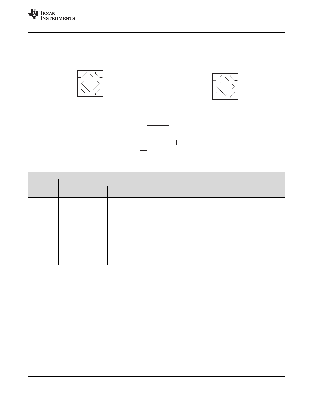
6 Pin Configuration and Functions
TPS3831, TPS3839
SBVS193D –JUNE 2012–REVISED JULY 2015
TPS3831 DQN Package
1-mm × 1-mm X2SON
Top View
TPS3839 DQN Package
1-mm × 1-mm X2SON
Top View
TPS3839 DBZ Package
SOT23-3
Top View
Pin Functions
PIN
NO.
NAME
TPS3839 TPS3839 TPS3831
(SOT23-3) (X2SON) (X2SON)
GND 1 3 3 — Ground
MR N/A N/A 2 I After the MR pin is deasserted, the RESET output deasserts after the
NC N/A 2 N/A — No internal connection.
RESET 2 1 1 O
Thermal pad N/A Available Available —
VDD 3 4 4 I Supply voltage
I/O DESCRIPTION
Manual reset. Pull this pin to a logic low to assert the RESET output.
reset delay (td) elapses.
Active-low reset output. RESET has a push-pull output drive and is
capable of directly driving input pins. RESET is low as long as V
remains below the factory threshold voltage, and until the delay time
(td) elapses after VDDrises above the threshold voltage.
Connect to ground or to a floating copper plane for mechanical
stability.
DD
Copyright © 2012–2015, Texas Instruments Incorporated Submit Documentation Feedback 5
TPS3831, TPS3839
SBVS193D –JUNE 2012–REVISED JULY 2015
www.ti.com
7 Specifications
7.1 Absolute Maximum Ratings
over operating free-air temperature range, unless otherwise noted
Voltage
Current RESET pin –10 10 mA
Temperature
(2)
(1) Stresses beyond those listed under Absolute Maximum Ratings may cause permanent damage to the device. These are stress ratings
only, and functional operation of the device at these or any other conditions beyond those indicated under Recommended Operating
Conditions is not implied. Exposure to absolute-maximum-rated conditions for extended periods may affect device reliability.
(2) As a result of the low dissipated power in this device, the junction temperature is assumed to be equal to the ambient temperature.
VDD, RESET –0.3 7 V
MR –0.3 VDD+ 0.3 V
Operating ambient, T
Storage, T
stg
A
7.2 ESD Ratings
V
(ESD)
Electrostatic discharge V
(1) JEDEC document JEP155 states that 500-V HBM allows safe manufacturing with a standard ESD control process.
(2) JEDEC document JEP157 states that 250-V CDM allows safe manufacturing with a standard ESD control process.
Human body model (HBM), per ANSI/ESDA/JEDEC JS-001
Charged device model (CDM), per JEDEC specification JESD22-C101
(1)
MIN MAX UNIT
–40 85
–65 150
°C
VALUE UNIT
(1)
(2)
±2000
±500
7.3 Recommended Operating Conditions
over operating free-air temperature range (unless otherwise noted)
MIN NOM MAX UNIT
V
DD
V
MR
V
RESET
I
RESET
Input supply voltage 0.9 6.5 V
Manual reset pin voltage 0 V
DD
V
RESET pin voltage 0 6.5 V
RESET pin current 0 8 mA
7.4 Thermal Information
TPS3839
THERMAL METRIC
(1)
DBZ (SOT23-3) DQN (X2SON)
3 PINS 4 PINS
R
θJA
R
θJC(top)
R
θJB
ψ
JT
ψ
JB
R
θJC(bot)
Junction-to-ambient thermal resistance 346.6 216.1 °C/W
Junction-to-case (top) thermal resistance 124.4 161.7 °C/W
Junction-to-board thermal resistance 78.9 162.1 °C/W
Junction-to-top characterization parameter 11.5 5.1 °C/W
Junction-to-board characterization parameter 77.3 161.7 °C/W
Junction-to-case (bottom) thermal resistance N/A 123.0 °C/W
(1) For more information about traditional and new thermal metrics, see the Semiconductor and IC Package Thermal Metrics application
report, SPRA953.
TPS3831,
TPS3839
UNIT
6 Submit Documentation Feedback Copyright © 2012–2015, Texas Instruments Incorporated
TPS3831, TPS3839
www.ti.com
SBVS193D –JUNE 2012–REVISED JULY 2015
7.5 Electrical Characteristics
At TA= –40°C to 85°C, 0.9 V < VDD< 6.5 V, and C1 = 0.1 µF, unless otherwise noted. Typical values are at 25°C.
PARAMETER TEST CONDITIONS MIN TYP MAX UNIT
V
V
I
DD
V
V
V
V
R
V
V
Input supply voltage 0.9 6.5 V
DD
Minimum VDDvoltage for valid output IOL= 1 µA 0.6 V
(POR)
Supply current (into VDD pin) Output not connected 150 500 nA
VDD= 0.9 V to 1.2 V, IOL= 120 µA 0.4
Low-level output voltage (RESET pin) VDD= 1.2 V to 2.8 V, IOL= 0.5 mA 0.4 V
OL
VDD= 2.8 V to 6.5 V, IOL= 2 mA 0.4
VDD= 0.9 V to 1.2 V, IOH= –50 µA VDD– 0.4
High-level output voltage (RESET pin) VDD= 1.2 V to 3.3 V, IOH= –0.5 mA VDD– 0.4 V
OH
VDD= 3.3 V to 6.5 V, IOH= –2 mA VDD– 0.4
Low-level input voltage (MR pin) 0.3V
IL
High-level input voltage (MR pin) 0.7V
IH
MR pin pullup resistance 10 20 30 kΩ
MR
DD
Negative-going input threshold accuracy TA= 25°C ±1%
TPS383xA09 0.874 0.9 0.914
TPS383xG12 1.073 1.1 1.117
TPS383xE16 1.482 1.52 1.543
TPS383xG18 1.628 1.67 1.695
Negative-going threshold voltage TPS3839G25 2.267 2.325 2.360 V
IT–
TPS383xL30 2.564 2.63 2.669
TPS383xK33 2.857 2.93 2.974
TPS383xG33 3.003 3.08 3.126
TPS383xK50 4.271 4.38 4.446
TPS383xA09 54
TPS383xG12 11
TPS383xE16 15
TPS383xG18 17
Hysteresis voltage TPS383xL30 26 mV
hys
TPS3839G25 23
TPS383xK33 29
TPS383xG33 31
TPS383xK50 44
DD
V
V
Copyright © 2012–2015, Texas Instruments Incorporated Submit Documentation Feedback 7
Time
V
IT-
+ V
HYS
V
IT-
0.7V
DD
0.3V
DD
MR
VDD
0.6 V
RESET
t
d
t
d
t
d
td= Reset Delay
= Undefined State
TPS3831, TPS3839
SBVS193D –JUNE 2012–REVISED JULY 2015
7.6 Timing Requirements
At TA= –40°C to 85°C, 0.9 V < VDD< 6.5 V, and C1 = 0.1 µF, unless otherwise noted. Typical values are at 25°C.
MIN TYP MAX UNIT
t
d
t
PD_VDD
t
PD_MR
RESET delay time (power-up delay) 120 200 350 ms
Propagation delay, VDDfalling (power-down delay) 20 µs
Propagation delay from MR low to RESET low 46 ns
www.ti.com
Figure 1. MR and VDD Reset Timing
8 Submit Documentation Feedback Copyright © 2012–2015, Texas Instruments Incorporated
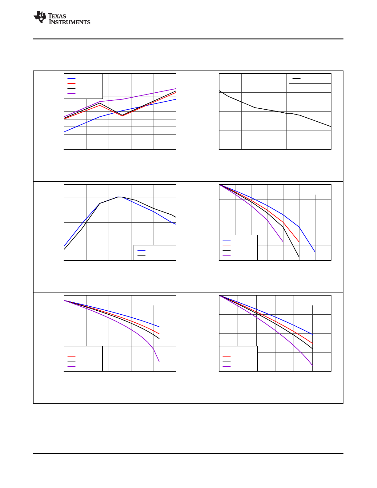
0.5
1.5
2.5
3.5
0 2 4 6 8 10
IOH (mA)
V
OH
(V)
TA = −40°C
TA = 0°C
TA = +25°C
TA = +85°C
VDD = 3.3 V
G005
2
2.5
3
3.5
4
0 2 4 6 8 10 12
IOH (mA)
V
OH
(V)
TA = −40°C
TA = 0°C
TA = +25°C
TA = +85°C
VDD =4.0 V
G006
−1
−0.8
−0.6
−0.4
−0.2
0
0.2
−40 −15 10 35 60 85
Temperature (°C)
Change in V
IT–
(%)
TPS3839A09
TPS3839K50
G003
0.8
1
1.2
1.4
1.6
1.8
0 0.5 1 1.5 2 2.5 3 3.5
IOH (mA)
V
OH
(V)
TA = −40°C
TA = 0°C
TA = +25°C
TA = +85°C
VDD = 1.8 V
G004
100
110
120
130
140
150
160
170
180
190
200
−40 −15 10 35 60 85
Temperature (°C)
Supply Current (nA)
VDD = 1.2 V
VDD = 3.3 V
VDD = 5.0 V
VDD = 6.5 V
G001
180
190
200
210
220
−40 −15 10 35 60 85
Temperature (°C)
Reset Delay Time (ms)
TPS3839K33
G002
www.ti.com
7.7 Typical Characteristics
At TA= 25°C and C1= 0.1 µF, unless otherwise noted.
Figure 2. Supply Current vs Temperature Figure 3. Reset Delay vs Temperature
TPS3831, TPS3839
SBVS193D –JUNE 2012–REVISED JULY 2015
Figure 4. Threshold Voltage vs Temperature Figure 5. VOHvs IOHand Temperature for VDD= 1.8 V
Copyright © 2012–2015, Texas Instruments Incorporated Submit Documentation Feedback 9
Figure 6. VOHvs IOHand Temperature for VDD= 3.3 V Figure 7. VOHvs IOHand Temperature for VDD= 4.0 V
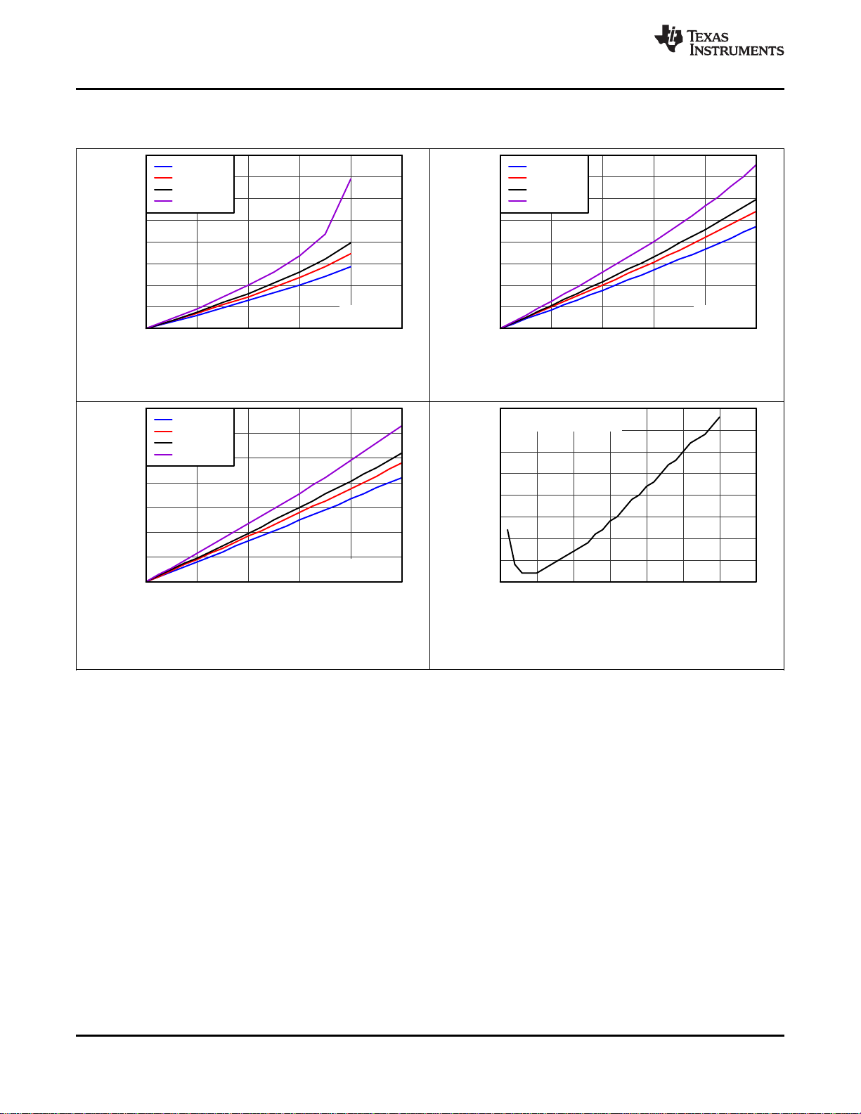
0
0.2
0.4
0.6
0.8
1
1.2
1.4
0 2 4 6 8 10
IOL (mA)
V
OL
(V)
TA = −40°C
TA = 0°C
TA = +25°C
TA = +85°C
VDD = 4.0 V
G009
10
15
20
25
30
35
40
45
50
0 5 10 15 20 25 30 35
VDD voltage drop below V
IT−
(%)
Minimum Pulse Duration Trigger Reset (µs)
Reset Occurs Above Line
G010
0
0.2
0.4
0.6
0.8
1
1.2
1.4
1.6
0 1 2 3 4 5
IOL (mA)
V
OL
(V)
TA = −40°C
TA = 0°C
TA = +25°C
TA = +25°C
VDD = 1.8 V
G007
0
0.2
0.4
0.6
0.8
1
1.2
1.4
1.6
0 2 4 6 8 10
IOL (mA)
V
OL
(V)
TA = −40°C
TA = 0°C
TA = +25°C
TA = +85°C
VDD = 3.3 V
G008
TPS3831, TPS3839
SBVS193D –JUNE 2012–REVISED JULY 2015
Typical Characteristics (continued)
At TA= 25°C and C1= 0.1 µF, unless otherwise noted.
Figure 8. VOLvs IOLand Temperature for VDD= 1.8 V Figure 9. VOLvs IOLand Temperature for VDD= 3.3 V
www.ti.com
Figure 10. VOLvs IOLand Temperature for VDD= 4.0 V Figure 11. Maximum Pulse Duration vs Percent of
10 Submit Documentation Feedback Copyright © 2012–2015, Texas Instruments Incorporated
Threshold Overdrive

Transient
Duration
(t )
Transient
Amplitude
V
DD
V
IT-
Delay
V
REF
VDD
GND
RESET
MR
( Only)TPS3831
VDD
TPS3831, TPS3839
www.ti.com
SBVS193D –JUNE 2012–REVISED JULY 2015
8 Detailed Description
8.1 Overview
The TPS3831 and TPS3839 are ultralow current voltage supervisory circuits that monitor the input supply voltage
of these devices. Both devices assert an active-low reset whenever the VDDsupply voltage drops below the
negative-going threshold voltage (V
200 ms after the VDDvoltage rises above the positive-going threshold voltage (V
designed to ignore fast transients on the VDD pin.
The TPS3831 device includes a manual reset input (MR) that can be used to force the RESET signal low, even if
the supply voltage is above V
IT–
.
8.2 Functional Block Diagram
). The output, RESET, remains asserted for approximately
IT–
IT–
+ V
). These devices are
hys
8.3 Feature Description
8.3.1 VDD Transient Rejection
The TPS383x (TPS3831 and TPS3839) devices have built-in rejection of fast transients on the VDD pin.
Transient rejection depends on both the duration and amplitude of the transient. Transient amplitude is measured
from the bottom of the transient to the negative threshold voltage (V
Figure 12. Voltage Transient Measurement
Copyright © 2012–2015, Texas Instruments Incorporated Submit Documentation Feedback 11
) of the device, as shown in Figure 12.
IT–

VDD
GND
TPS3831
20 kW
MR
10
15
20
25
30
35
40
45
50
0 5 10 15 20 25 30 35
VDD voltage drop below V
IT−
(%)
Minimum Pulse Duration Trigger Reset (µs)
Reset Occurs Above Line
G010
TPS3831, TPS3839
SBVS193D –JUNE 2012–REVISED JULY 2015
www.ti.com
Feature Description (continued)
Figure 13 shows the relationship between the transient amplitude and duration required to trigger a reset. Any
combination of duration and amplitude greater than that shown in Figure 13 generates a reset signal.
Figure 13. TPS3839 Transient Rejection
8.3.2 Manual Reset (MR) Input (TPS3831 Only)
The manual reset (MR) input allows a processor, or other logic devices, to initiate a reset (TPS3831 device only).
A logic low (0.3 VDD) on MR causes RESET to assert. After MR returns to a logic high and VDDis greater than
the threshold voltage, RESET is deasserted after the reset delay time, td, elapses. MR is internally tied to VDD
with a 20-kΩ resistor; therefore, this pin can be left unconnected if MR is not used. If a logic signal driving MR
does not go fully to VDD, some additional current draws into VDD as a result of the internal pullup resistor on MR.
To minimize current draw, a logic-level FET can be used, as shown in Figure 14.
Figure 14. Using a Logic-Level FET to Minimize Current Draw
8.4 Device Functional Modes
8.4.1 Normal Operation (VDD> V
When the voltage on VDD is greater than V
relative to V
8.4.2 Below V
When the voltage on VDD is less than V
output is asserted.
8.4.3 Below Power-On Reset (VDD< V
When the voltage on VDD is lower than the power-on reset voltage (V
not rely on the RESET output for proper device function under this condition.
12 Submit Documentation Feedback Copyright © 2012–2015, Texas Instruments Incorporated
.
IT–
DD(min)(V(POR)
DD(min)
< VDD< V
DD(min)
DD(min)
(POR)
)
, the RESET output corresponds to the voltage on the VDD pin
DD(min)
but greater than the power-on reset voltage (V
), the RESET output is undefined. Do
(POR)
), the RESET
(POR)

4.7 PH
10 PF
10 PF
5 k:
L
VIN VOUT
RI
GND
FB
EN
One-Cell
Alkaline
VDD
GND
RESET
TPS3839A09
3.3 V at 40 mA
TPS61261
TPS3831, TPS3839
www.ti.com
SBVS193D –JUNE 2012–REVISED JULY 2015
9 Applications and Implementation
NOTE
Information in the following applications sections is not part of the TI component
specification, and TI does not warrant its accuracy or completeness. TI’s customers are
responsible for determining suitability of components for their purposes. Customers should
validate and test their design implementation to confirm system functionality.
9.1 Application Information
Low operating voltage and threshold options make the TPS383x devices well-suited for monitoring single-cell,
alkaline-battery applications.
9.2 Typical Application
Figure 15 shows the TPS3839A09 used to disable a boost converter when the cell voltage reaches 0.9 V, which
is the end of the discharge voltage for a single alkaline battery cell. When the cell voltage reaches 0.9 V, the
TPS61261 enable pin is driven low. This setting disables the TPS61261 and places it in a low-current shutdown
state. The combination of the TPS3839 and TPS61261 devices consumes only 250 nA (typical) from the
discharged battery.
Figure 15. Disabled Boost Converter
9.2.1 Design Requirements
Table 1 lists the design requirements for Figure 15.
Table 1. Design Requirements and Results
DESIGN REQUIREMENTS
Input voltage range of 0.9 V to 1.7 V 0.9 V to 6.5 V 0.8 V to 4 V 0.9 V to 4 V
Shutdown current < 3 µA 0.5 μA (maximum) 1.5 μA (maximum) 2.0 μA (maximum)
Output voltage of 3.3 V N/A 3.3 V 3.3 V
Output current of 50 mA N/A 100 mA 100 mA
Switching frequency ≥ 1 MHz N/A 2.5 MHz 2.5 MHz
Copyright © 2012–2015, Texas Instruments Incorporated Submit Documentation Feedback 13
TPS3839A09 TPS61261 COMBINED
DESIGN RESULT

100
110
120
130
140
150
160
170
180
190
200
−40 −15 10 35 60 85
Temperature (°C)
Supply Current (nA)
VDD = 1.2 V
VDD = 3.3 V
VDD = 5.0 V
VDD = 6.5 V
G001
RESET
GND
TPS3839K33
VDD
RST
Microprocessor
3.3 V
V
CC
47 k:
TPS3831, TPS3839
SBVS193D –JUNE 2012–REVISED JULY 2015
www.ti.com
9.2.2 Detailed Design Procedure
9.2.2.1 Input Capacitor
The TPS383x devices use a unique sampling scheme to maintain an extremely low average quiescent current of
150 nA. The TPS383x devices typically consume only approximately 100 nA of dc current. However, this current
rises to approximately 15 µA for about 200 µs when the TPS383x devices sample the input voltage. If the source
impedance back to the supply voltage is high, then the additional current during sampling may trigger a false
reset as a result of the apparent voltage drop at VDD. For applications with high-impedance input supplies
(including trace impedance), TI recommends adding a small 0.1-µF bypass capacitor near the TPS3839 VDD
pin. This bypass capacitor effectively keeps the average current at 150 nA and reduces the effects of a highimpedance voltage source.
9.2.2.2 Bidirectional Reset Pins
Some devices have bidirectional reset pins that act both as an input and an output. For applications where the
TPS383x devices drive a bidirectional reset pin, place a series resistor between the TPS383x output and the
reset pin to protect against excessive current flow when both the TPS383x devices and the reset pin attempt to
drive the reset line. Figure 16 shows the connection of the TPS3839K33 to a bidirectional reset pin of a
microcontroller using a series resistor.
9.2.3 Application Curve
14 Submit Documentation Feedback Copyright © 2012–2015, Texas Instruments Incorporated
Figure 16. Connection to a Bidirectional Reset Pin
Figure 17. Supply Current vs Temperature

Input
Supply
1
2
RESET
Flag
3
C
VDD
TPS3831, TPS3839
www.ti.com
SBVS193D –JUNE 2012–REVISED JULY 2015
10 Power Supply Recommendations
These devices are designed to operate from an input supply with a voltage range between 0.9 V and 6.5 V. Use
a low-impedance power supply to eliminate inaccuracies caused by the extra current during the input-voltage
sampling discussed in the Input Capacitor section.
11 Layout
11.1 Layout Guidelines
Make sure the connection to the VDD pin is low impedance and able to carry 15 µA without a significant voltage
drop. Place a 0.1-µF bypass capacitor near the VDD pin if the 15-µA sampling current causes too much voltage
droop.
11.2 Layout Example
Figure 18. Recommended Layout
Copyright © 2012–2015, Texas Instruments Incorporated Submit Documentation Feedback 15

TPS3831, TPS3839
SBVS193D –JUNE 2012–REVISED JULY 2015
www.ti.com
12 Device and Documentation Support
12.1 Device Support
12.1.1 Development Support
12.1.1.1 Evaluation Modules
Two evaluation modules (EVMs) are available to assist in the initial circuit performance evaluation using the
TPS3831 and TPS3839. The TPS3831G33EVM-187 and TPS3839K33EVM-112 evaluation modules (and
related user's guides) can be requested at the TI website through the product folders or purchased directly from
the TI eStore.
12.1.1.2 Spice Models
Computer simulation of circuit performance using SPICE is often useful when analyzing the performance of
analog circuits and systems. SPICE models for the TPS3831 and TPS3839 devices are available through each
of the product folders under Tools & Software.
12.2 Documentation Support
12.2.1 Related Documentation
• TPS3831G33EVM-187 User's Guide, SLVU774
• TPS3839K33EVM-112 User's Guide, SLVU758.
• TPS61261 Data Sheet, SLVSA99
12.3 Related Links
Table 2 lists quick access links. Categories include technical documents, support and community resources,
tools and software, and quick access to sample or buy.
Table 2. Related Links
PARTS PRODUCT FOLDER SAMPLE & BUY
TPS3831 Click here Click here Click here Click here Click here
TPS3839 Click here Click here Click here Click here Click here
TECHNICAL TOOLS & SUPPORT &
DOCUMENTS SOFTWARE COMMUNITY
12.4 Community Resources
The following links connect to TI community resources. Linked contents are provided "AS IS" by the respective
contributors. They do not constitute TI specifications and do not necessarily reflect TI's views; see TI's Terms of
Use.
TI E2E™ Online Community TI's Engineer-to-Engineer (E2E) Community. Created to foster collaboration
among engineers. At e2e.ti.com, you can ask questions, share knowledge, explore ideas and help
solve problems with fellow engineers.
Design Support TI's Design Support Quickly find helpful E2E forums along with design support tools and
contact information for technical support.
12.5 Trademarks
E2E is a trademark of Texas Instruments.
All other trademarks are the property of their respective owners.
12.6 Electrostatic Discharge Caution
These devices have limited built-in ESD protection. The leads should be shorted together or the device placed in conductive foam
during storage or handling to prevent electrostatic damage to the MOS gates.
16 Submit Documentation Feedback Copyright © 2012–2015, Texas Instruments Incorporated

TPS3831, TPS3839
www.ti.com
SBVS193D –JUNE 2012–REVISED JULY 2015
12.7 Glossary
SLYZ022 — TI Glossary.
This glossary lists and explains terms, acronyms, and definitions.
13 Mechanical, Packaging, and Orderable Information
The following pages include mechanical, packaging, and orderable information. This information is the most
current data available for the designated devices. This data is subject to change without notice and revision of
this document. For browser-based versions of this data sheet, refer to the left-hand navigation.
Copyright © 2012–2015, Texas Instruments Incorporated Submit Documentation Feedback 17

PACKAGE OPTION ADDENDUM
www.ti.com
PACKAGING INFORMATION
Orderable Device Status
TPS3831A09DQNR ACTIVE X2SON DQN 4 3000 Green (RoHS
TPS3831A09DQNT ACTIVE X2SON DQN 4 250 Green (RoHS
TPS3831E16DQNR ACTIVE X2SON DQN 4 3000 Green (RoHS
TPS3831E16DQNT ACTIVE X2SON DQN 4 250 Green (RoHS
TPS3831G12DQNR ACTIVE X2SON DQN 4 3000 Green (RoHS
TPS3831G12DQNT ACTIVE X2SON DQN 4 250 Green (RoHS
TPS3831G18DQNR ACTIVE X2SON DQN 4 3000 Green (RoHS
TPS3831G18DQNT ACTIVE X2SON DQN 4 250 Green (RoHS
TPS3831G33DQNR ACTIVE X2SON DQN 4 3000 Green (RoHS
TPS3831G33DQNT ACTIVE X2SON DQN 4 250 Green (RoHS
TPS3831K33DQNR ACTIVE X2SON DQN 4 3000 Green (RoHS
TPS3831K33DQNT ACTIVE X2SON DQN 4 250 Green (RoHS
TPS3831K50DQNR ACTIVE X2SON DQN 4 3000 Green (RoHS
TPS3831K50DQNT ACTIVE X2SON DQN 4 250 Green (RoHS
TPS3831L30DQNR ACTIVE X2SON DQN 4 3000 Green (RoHS
TPS3831L30DQNT ACTIVE X2SON DQN 4 250 Green (RoHS
TPS3839A09DBZR ACTIVE SOT-23 DBZ 3 3000 Green (RoHS
Package Type Package
(1)
Drawing
Pins Package
Qty
Eco Plan
(2)
& no Sb/Br)
& no Sb/Br)
& no Sb/Br)
& no Sb/Br)
& no Sb/Br)
& no Sb/Br)
& no Sb/Br)
& no Sb/Br)
& no Sb/Br)
& no Sb/Br)
& no Sb/Br)
& no Sb/Br)
& no Sb/Br)
& no Sb/Br)
& no Sb/Br)
& no Sb/Br)
& no Sb/Br)
Lead/Ball Finish
(6)
MSL Peak Temp
(3)
Op Temp (°C) Device Marking
CU NIPDAU Level-1-260C-UNLIM -40 to 85 A3
CU NIPDAU Level-1-260C-UNLIM -40 to 85 A3
CU NIPDAU Level-1-260C-UNLIM -40 to 85 A5
CU NIPDAU Level-1-260C-UNLIM -40 to 85 A5
CU NIPDAU Level-1-260C-UNLIM -40 to 85 A4
CU NIPDAU Level-1-260C-UNLIM -40 to 85 A4
CU NIPDAU Level-1-260C-UNLIM -40 to 85 A6
CU NIPDAU Level-1-260C-UNLIM -40 to 85 A6
CU NIPDAU Level-1-260C-UNLIM -40 to 85 A7
CU NIPDAU Level-1-260C-UNLIM -40 to 85 A7
CU NIPDAU Level-1-260C-UNLIM -40 to 85 A8
CU NIPDAU Level-1-260C-UNLIM -40 to 85 A8
CU NIPDAU Level-1-260C-UNLIM -40 to 85 A9
CU NIPDAU Level-1-260C-UNLIM -40 to 85 A9
CU NIPDAU Level-1-260C-UNLIM -40 to 85 BA
CU NIPDAU Level-1-260C-UNLIM -40 to 85 BA
CU NIPDAU Level-1-260C-UNLIM -40 to 85 PZDI
9-Jul-2015
Samples
(4/5)
Addendum-Page 1

PACKAGE OPTION ADDENDUM
www.ti.com
Orderable Device Status
Package Type Package
(1)
Drawing
Pins Package
Qty
TPS3839A09DBZT ACTIVE SOT-23 DBZ 3 250 Green (RoHS
TPS3839A09DQNR ACTIVE X2SON DQN 4 3000 Green (RoHS
TPS3839A09DQNT ACTIVE X2SON DQN 4 250 Green (RoHS
TPS3839E16DBZR ACTIVE SOT-23 DBZ 3 3000 Green (RoHS
TPS3839E16DBZT ACTIVE SOT-23 DBZ 3 250 Green (RoHS
TPS3839E16DQNR ACTIVE X2SON DQN 4 3000 Green (RoHS
TPS3839E16DQNT ACTIVE X2SON DQN 4 250 Green (RoHS
TPS3839G12DBZR ACTIVE SOT-23 DBZ 3 3000 Green (RoHS
TPS3839G12DBZT ACTIVE SOT-23 DBZ 3 250 Green (RoHS
TPS3839G12DQNR ACTIVE X2SON DQN 4 3000 Green (RoHS
TPS3839G12DQNT ACTIVE X2SON DQN 4 250 Green (RoHS
TPS3839G18DBZR ACTIVE SOT-23 DBZ 3 3000 Green (RoHS
TPS3839G18DBZT ACTIVE SOT-23 DBZ 3 250 Green (RoHS
TPS3839G18DQNR ACTIVE X2SON DQN 4 3000 Green (RoHS
TPS3839G18DQNT ACTIVE X2SON DQN 4 250 Green (RoHS
TPS3839G25DBZR ACTIVE SOT-23 DBZ 3 3000 Green (RoHS
TPS3839G25DBZT ACTIVE SOT-23 DBZ 3 250 Green (RoHS
TPS3839G33DBZR ACTIVE SOT-23 DBZ 3 3000 Green (RoHS
Eco Plan
(2)
& no Sb/Br)
& no Sb/Br)
& no Sb/Br)
& no Sb/Br)
& no Sb/Br)
& no Sb/Br)
& no Sb/Br)
& no Sb/Br)
& no Sb/Br)
& no Sb/Br)
& no Sb/Br)
& no Sb/Br)
& no Sb/Br)
& no Sb/Br)
& no Sb/Br)
& no Sb/Br)
& no Sb/Br)
& no Sb/Br)
Lead/Ball Finish
(6)
MSL Peak Temp
(3)
Op Temp (°C) Device Marking
CU NIPDAU Level-1-260C-UNLIM -40 to 85 PZDI
CU NIPDAU Level-1-260C-UNLIM -40 to 85 ZJ
CU NIPDAU Level-1-260C-UNLIM -40 to 85 ZJ
CU NIPDAU Level-1-260C-UNLIM -40 to 85 PZCI
CU NIPDAU Level-1-260C-UNLIM -40 to 85 PZCI
CU NIPDAU Level-1-260C-UNLIM -40 to 85 ZK
CU NIPDAU Level-1-260C-UNLIM -40 to 85 ZK
CU NIPDAU Level-1-260C-UNLIM -40 to 85 PZBI
CU NIPDAU Level-1-260C-UNLIM -40 to 85 PZBI
CU NIPDAU Level-1-260C-UNLIM -40 to 85 ZE
CU NIPDAU Level-1-260C-UNLIM -40 to 85 ZE
CU NIPDAU Level-1-260C-UNLIM -40 to 85 PZAI
CU NIPDAU Level-1-260C-UNLIM -40 to 85 PZAI
CU NIPDAU Level-1-260C-UNLIM -40 to 85 ZL
CU NIPDAU Level-1-260C-UNLIM -40 to 85 ZL
CU NIPDAU Level-1-260C-UNLIM -40 to 85 PZNI
CU NIPDAU Level-1-260C-UNLIM -40 to 85 PZNI
CU NIPDAU Level-1-260C-UNLIM -40 to 85 PYZI
9-Jul-2015
Samples
(4/5)
Addendum-Page 2

PACKAGE OPTION ADDENDUM
www.ti.com
Orderable Device Status
TPS3839G33DBZT ACTIVE SOT-23 DBZ 3 250 Green (RoHS
Package Type Package
(1)
Drawing
Pins Package
Qty
Eco Plan
(2)
Lead/Ball Finish
(6)
MSL Peak Temp
(3)
CU NIPDAU Level-1-260C-UNLIM -40 to 85 PYZI
& no Sb/Br)
TPS3839G33DQNR ACTIVE X2SON DQN 4 3000 Green (RoHS
CU NIPDAU Level-1-260C-UNLIM -40 to 85 ZG
& no Sb/Br)
TPS3839G33DQNT ACTIVE X2SON DQN 4 250 Green (RoHS
CU NIPDAU Level-1-260C-UNLIM -40 to 85 ZG
& no Sb/Br)
TPS3839K33DBZR ACTIVE SOT-23 DBZ 3 3000 Green (RoHS
CU NIPDAU Level-1-260C-UNLIM -40 to 85 PYYI
& no Sb/Br)
TPS3839K33DBZT ACTIVE SOT-23 DBZ 3 250 Green (RoHS
CU NIPDAU Level-1-260C-UNLIM -40 to 85 PYYI
& no Sb/Br)
TPS3839K33DQNR ACTIVE X2SON DQN 4 3000 Green (RoHS
CU NIPDAU Level-1-260C-UNLIM -40 to 85 ZF
& no Sb/Br)
TPS3839K33DQNT ACTIVE X2SON DQN 4 250 Green (RoHS
CU NIPDAU Level-1-260C-UNLIM -40 to 85 ZF
& no Sb/Br)
TPS3839K50DBZR ACTIVE SOT-23 DBZ 3 3000 Green (RoHS
CU NIPDAU Level-1-260C-UNLIM -40 to 85 PYXI
& no Sb/Br)
TPS3839K50DBZT ACTIVE SOT-23 DBZ 3 250 Green (RoHS
CU NIPDAU Level-1-260C-UNLIM -40 to 85 PYXI
& no Sb/Br)
TPS3839K50DQNR ACTIVE X2SON DQN 4 3000 Green (RoHS
CU NIPDAU Level-1-260C-UNLIM -40 to 85 ZH
& no Sb/Br)
TPS3839K50DQNT ACTIVE X2SON DQN 4 250 Green (RoHS
CU NIPDAU Level-1-260C-UNLIM -40 to 85 ZH
& no Sb/Br)
TPS3839L30DBZR ACTIVE SOT-23 DBZ 3 3000 Green (RoHS
CU NIPDAU Level-1-260C-UNLIM -40 to 85 PYWI
& no Sb/Br)
TPS3839L30DBZT ACTIVE SOT-23 DBZ 3 250 Green (RoHS
CU NIPDAU Level-1-260C-UNLIM -40 to 85 PYWI
& no Sb/Br)
TPS3839L30DQNR ACTIVE X2SON DQN 4 3000 Green (RoHS
CU NIPDAU Level-1-260C-UNLIM -40 to 85 ZI
& no Sb/Br)
TPS3839L30DQNT ACTIVE X2SON DQN 4 250 Green (RoHS
CU NIPDAU Level-1-260C-UNLIM -40 to 85 ZI
& no Sb/Br)
(1)
The marketing status values are defined as follows:
ACTIVE: Product device recommended for new designs.
LIFEBUY: TI has announced that the device will be discontinued, and a lifetime-buy period is in effect.
NRND: Not recommended for new designs. Device is in production to support existing customers, but TI does not recommend using this part in a new design.
PREVIEW: Device has been announced but is not in production. Samples may or may not be available.
OBSOLETE: TI has discontinued the production of the device.
9-Jul-2015
Op Temp (°C) Device Marking
(4/5)
Samples
Addendum-Page 3

PACKAGE OPTION ADDENDUM
www.ti.com
(2)
Eco Plan - The planned eco-friendly classification: Pb-Free (RoHS), Pb-Free (RoHS Exempt), or Green (RoHS & no Sb/Br) - please check http://www.ti.com/productcontent for the latest availability
information and additional product content details.
TBD: The Pb-Free/Green conversion plan has not been defined.
Pb-Free (RoHS): TI's terms "Lead-Free" or "Pb-Free" mean semiconductor products that are compatible with the current RoHS requirements for all 6 substances, including the requirement that
lead not exceed 0.1% by weight in homogeneous materials. Where designed to be soldered at high temperatures, TI Pb-Free products are suitable for use in specified lead-free processes.
Pb-Free (RoHS Exempt): This component has a RoHS exemption for either 1) lead-based flip-chip solder bumps used between the die and package, or 2) lead-based die adhesive used between
the die and leadframe. The component is otherwise considered Pb-Free (RoHS compatible) as defined above.
Green (RoHS & no Sb/Br): TI defines "Green" to mean Pb-Free (RoHS compatible), and free of Bromine (Br) and Antimony (Sb) based flame retardants (Br or Sb do not exceed 0.1% by weight
in homogeneous material)
(3)
MSL, Peak Temp. - The Moisture Sensitivity Level rating according to the JEDEC industry standard classifications, and peak solder temperature.
(4)
There may be additional marking, which relates to the logo, the lot trace code information, or the environmental category on the device.
(5)
Multiple Device Markings will be inside parentheses. Only one Device Marking contained in parentheses and separated by a "~" will appear on a device. If a line is indented then it is a continuation
of the previous line and the two combined represent the entire Device Marking for that device.
(6)
Lead/Ball Finish - Orderable Devices may have multiple material finish options. Finish options are separated by a vertical ruled line. Lead/Ball Finish values may wrap to two lines if the finish
value exceeds the maximum column width.
Important Information and Disclaimer:The information provided on this page represents TI's knowledge and belief as of the date that it is provided. TI bases its knowledge and belief on information
provided by third parties, and makes no representation or warranty as to the accuracy of such information. Efforts are underway to better integrate information from third parties. TI has taken and
continues to take reasonable steps to provide representative and accurate information but may not have conducted destructive testing or chemical analysis on incoming materials and chemicals.
TI and TI suppliers consider certain information to be proprietary, and thus CAS numbers and other limited information may not be available for release.
In no event shall TI's liability arising out of such information exceed the total purchase price of the TI part(s) at issue in this document sold by TI to Customer on an annual basis.
9-Jul-2015
Addendum-Page 4

PACKAGE MATERIALS INFORMATION
www.ti.com 9-Jul-2015
TAPE AND REEL INFORMATION
*All dimensions are nominal
Device Package
Type
TPS3831A09DQNR X2SON DQN 4 3000 180.0 9.5 1.16 1.16 0.63 4.0 8.0 Q2
TPS3831A09DQNT X2SON DQN 4 250 180.0 9.5 1.16 1.16 0.63 4.0 8.0 Q2
TPS3831E16DQNR X2SON DQN 4 3000 180.0 9.5 1.16 1.16 0.63 4.0 8.0 Q2
TPS3831E16DQNT X2SON DQN 4 250 180.0 9.5 1.16 1.16 0.63 4.0 8.0 Q2
TPS3831G12DQNR X2SON DQN 4 3000 180.0 9.5 1.16 1.16 0.63 4.0 8.0 Q2
TPS3831G12DQNT X2SON DQN 4 250 180.0 9.5 1.16 1.16 0.63 4.0 8.0 Q2
TPS3831G18DQNR X2SON DQN 4 3000 180.0 9.5 1.16 1.16 0.63 4.0 8.0 Q2
TPS3831G18DQNT X2SON DQN 4 250 180.0 9.5 1.16 1.16 0.63 4.0 8.0 Q2
TPS3831G33DQNR X2SON DQN 4 3000 180.0 9.5 1.16 1.16 0.63 4.0 8.0 Q2
TPS3831G33DQNT X2SON DQN 4 250 180.0 9.5 1.16 1.16 0.63 4.0 8.0 Q2
TPS3831K33DQNR X2SON DQN 4 3000 180.0 9.5 1.16 1.16 0.63 4.0 8.0 Q2
TPS3831K33DQNT X2SON DQN 4 250 180.0 9.5 1.16 1.16 0.63 4.0 8.0 Q2
TPS3831K50DQNR X2SON DQN 4 3000 180.0 9.5 1.16 1.16 0.63 4.0 8.0 Q2
TPS3831K50DQNT X2SON DQN 4 250 180.0 9.5 1.16 1.16 0.63 4.0 8.0 Q2
TPS3831L30DQNR X2SON DQN 4 3000 180.0 9.5 1.16 1.16 0.63 4.0 8.0 Q2
TPS3831L30DQNT X2SON DQN 4 250 180.0 9.5 1.16 1.16 0.63 4.0 8.0 Q2
TPS3839A09DBZR SOT-23 DBZ 3 3000 179.0 8.4 3.15 2.95 1.22 4.0 8.0 Q3
TPS3839A09DBZT SOT-23 DBZ 3 250 179.0 8.4 3.15 2.95 1.22 4.0 8.0 Q3
Package
Drawing
Pins SPQ Reel
Diameter
(mm)
Reel
Width
W1 (mm)
A0
(mm)B0(mm)K0(mm)P1(mm)W(mm)
Pin1
Quadrant
Pack Materials-Page 1

PACKAGE MATERIALS INFORMATION
www.ti.com 9-Jul-2015
Device Package
Type
TPS3839A09DQNR X2SON DQN 4 3000 180.0 9.5 1.16 1.16 0.63 4.0 8.0 Q2
TPS3839A09DQNT X2SON DQN 4 250 180.0 9.5 1.16 1.16 0.63 4.0 8.0 Q2
TPS3839E16DBZR SOT-23 DBZ 3 3000 179.0 8.4 3.15 2.95 1.22 4.0 8.0 Q3
TPS3839E16DBZT SOT-23 DBZ 3 250 179.0 8.4 3.15 2.95 1.22 4.0 8.0 Q3
TPS3839E16DQNR X2SON DQN 4 3000 180.0 9.5 1.16 1.16 0.63 4.0 8.0 Q2
TPS3839E16DQNT X2SON DQN 4 250 180.0 9.5 1.16 1.16 0.63 4.0 8.0 Q2
TPS3839G12DBZR SOT-23 DBZ 3 3000 179.0 8.4 3.15 2.95 1.22 4.0 8.0 Q3
TPS3839G12DBZT SOT-23 DBZ 3 250 179.0 8.4 3.15 2.95 1.22 4.0 8.0 Q3
TPS3839G12DQNR X2SON DQN 4 3000 180.0 9.5 1.16 1.16 0.63 4.0 8.0 Q2
TPS3839G12DQNT X2SON DQN 4 250 180.0 9.5 1.16 1.16 0.63 4.0 8.0 Q2
TPS3839G18DBZR SOT-23 DBZ 3 3000 179.0 8.4 3.15 2.95 1.22 4.0 8.0 Q3
TPS3839G18DBZT SOT-23 DBZ 3 250 179.0 8.4 3.15 2.95 1.22 4.0 8.0 Q3
TPS3839G18DQNR X2SON DQN 4 3000 180.0 9.5 1.16 1.16 0.63 4.0 8.0 Q2
TPS3839G18DQNT X2SON DQN 4 250 180.0 9.5 1.16 1.16 0.63 4.0 8.0 Q2
TPS3839G25DBZR SOT-23 DBZ 3 3000 179.0 8.4 3.15 2.95 1.22 4.0 8.0 Q3
TPS3839G25DBZT SOT-23 DBZ 3 250 179.0 8.4 3.15 2.95 1.22 4.0 8.0 Q3
TPS3839G33DBZR SOT-23 DBZ 3 3000 179.0 8.4 3.15 2.95 1.22 4.0 8.0 Q3
TPS3839G33DBZT SOT-23 DBZ 3 250 179.0 8.4 3.15 2.95 1.22 4.0 8.0 Q3
TPS3839G33DQNR X2SON DQN 4 3000 180.0 9.5 1.16 1.16 0.63 4.0 8.0 Q2
TPS3839G33DQNT X2SON DQN 4 250 180.0 9.5 1.16 1.16 0.63 4.0 8.0 Q2
TPS3839K33DBZR SOT-23 DBZ 3 3000 179.0 8.4 3.15 2.95 1.22 4.0 8.0 Q3
TPS3839K33DBZT SOT-23 DBZ 3 250 179.0 8.4 3.15 2.95 1.22 4.0 8.0 Q3
TPS3839K33DQNR X2SON DQN 4 3000 180.0 9.5 1.16 1.16 0.63 4.0 8.0 Q2
TPS3839K33DQNT X2SON DQN 4 250 180.0 9.5 1.16 1.16 0.63 4.0 8.0 Q2
TPS3839K50DBZR SOT-23 DBZ 3 3000 179.0 8.4 3.15 2.95 1.22 4.0 8.0 Q3
TPS3839K50DBZT SOT-23 DBZ 3 250 179.0 8.4 3.15 2.95 1.22 4.0 8.0 Q3
TPS3839K50DQNR X2SON DQN 4 3000 180.0 9.5 1.16 1.16 0.63 4.0 8.0 Q2
TPS3839K50DQNT X2SON DQN 4 250 180.0 9.5 1.16 1.16 0.63 4.0 8.0 Q2
TPS3839L30DBZR SOT-23 DBZ 3 3000 179.0 8.4 3.15 2.95 1.22 4.0 8.0 Q3
TPS3839L30DBZT SOT-23 DBZ 3 250 179.0 8.4 3.15 2.95 1.22 4.0 8.0 Q3
TPS3839L30DQNR X2SON DQN 4 3000 180.0 9.5 1.16 1.16 0.63 4.0 8.0 Q2
TPS3839L30DQNT X2SON DQN 4 250 180.0 9.5 1.16 1.16 0.63 4.0 8.0 Q2
Package
Drawing
Pins SPQ Reel
Diameter
(mm)
Reel
Width
W1 (mm)
A0
(mm)B0(mm)K0(mm)P1(mm)W(mm)
Pin1
Quadrant
Pack Materials-Page 2

PACKAGE MATERIALS INFORMATION
www.ti.com 9-Jul-2015
*All dimensions are nominal
Device Package Type Package Drawing Pins SPQ Length (mm) Width (mm) Height (mm)
TPS3831A09DQNR X2SON DQN 4 3000 184.0 184.0 19.0
TPS3831A09DQNT X2SON DQN 4 250 184.0 184.0 19.0
TPS3831E16DQNR X2SON DQN 4 3000 184.0 184.0 19.0
TPS3831E16DQNT X2SON DQN 4 250 184.0 184.0 19.0
TPS3831G12DQNR X2SON DQN 4 3000 184.0 184.0 19.0
TPS3831G12DQNT X2SON DQN 4 250 184.0 184.0 19.0
TPS3831G18DQNR X2SON DQN 4 3000 184.0 184.0 19.0
TPS3831G18DQNT X2SON DQN 4 250 184.0 184.0 19.0
TPS3831G33DQNR X2SON DQN 4 3000 184.0 184.0 19.0
TPS3831G33DQNT X2SON DQN 4 250 184.0 184.0 19.0
TPS3831K33DQNR X2SON DQN 4 3000 184.0 184.0 19.0
TPS3831K33DQNT X2SON DQN 4 250 184.0 184.0 19.0
TPS3831K50DQNR X2SON DQN 4 3000 184.0 184.0 19.0
TPS3831K50DQNT X2SON DQN 4 250 184.0 184.0 19.0
TPS3831L30DQNR X2SON DQN 4 3000 184.0 184.0 19.0
TPS3831L30DQNT X2SON DQN 4 250 184.0 184.0 19.0
TPS3839A09DBZR SOT-23 DBZ 3 3000 203.0 203.0 35.0
TPS3839A09DBZT SOT-23 DBZ 3 250 203.0 203.0 35.0
TPS3839A09DQNR X2SON DQN 4 3000 184.0 184.0 19.0
TPS3839A09DQNT X2SON DQN 4 250 184.0 184.0 19.0
Pack Materials-Page 3

PACKAGE MATERIALS INFORMATION
www.ti.com 9-Jul-2015
Device Package Type Package Drawing Pins SPQ Length (mm) Width (mm) Height (mm)
TPS3839E16DBZR SOT-23 DBZ 3 3000 203.0 203.0 35.0
TPS3839E16DBZT SOT-23 DBZ 3 250 203.0 203.0 35.0
TPS3839E16DQNR X2SON DQN 4 3000 184.0 184.0 19.0
TPS3839E16DQNT X2SON DQN 4 250 184.0 184.0 19.0
TPS3839G12DBZR SOT-23 DBZ 3 3000 203.0 203.0 35.0
TPS3839G12DBZT SOT-23 DBZ 3 250 203.0 203.0 35.0
TPS3839G12DQNR X2SON DQN 4 3000 184.0 184.0 19.0
TPS3839G12DQNT X2SON DQN 4 250 184.0 184.0 19.0
TPS3839G18DBZR SOT-23 DBZ 3 3000 203.0 203.0 35.0
TPS3839G18DBZT SOT-23 DBZ 3 250 203.0 203.0 35.0
TPS3839G18DQNR X2SON DQN 4 3000 184.0 184.0 19.0
TPS3839G18DQNT X2SON DQN 4 250 184.0 184.0 19.0
TPS3839G25DBZR SOT-23 DBZ 3 3000 203.0 203.0 35.0
TPS3839G25DBZT SOT-23 DBZ 3 250 203.0 203.0 35.0
TPS3839G33DBZR SOT-23 DBZ 3 3000 203.0 203.0 35.0
TPS3839G33DBZT SOT-23 DBZ 3 250 203.0 203.0 35.0
TPS3839G33DQNR X2SON DQN 4 3000 184.0 184.0 19.0
TPS3839G33DQNT X2SON DQN 4 250 184.0 184.0 19.0
TPS3839K33DBZR SOT-23 DBZ 3 3000 203.0 203.0 35.0
TPS3839K33DBZT SOT-23 DBZ 3 250 203.0 203.0 35.0
TPS3839K33DQNR X2SON DQN 4 3000 184.0 184.0 19.0
TPS3839K33DQNT X2SON DQN 4 250 184.0 184.0 19.0
TPS3839K50DBZR SOT-23 DBZ 3 3000 203.0 203.0 35.0
TPS3839K50DBZT SOT-23 DBZ 3 250 203.0 203.0 35.0
TPS3839K50DQNR X2SON DQN 4 3000 184.0 184.0 19.0
TPS3839K50DQNT X2SON DQN 4 250 184.0 184.0 19.0
TPS3839L30DBZR SOT-23 DBZ 3 3000 203.0 203.0 35.0
TPS3839L30DBZT SOT-23 DBZ 3 250 203.0 203.0 35.0
TPS3839L30DQNR X2SON DQN 4 3000 184.0 184.0 19.0
TPS3839L30DQNT X2SON DQN 4 250 184.0 184.0 19.0
Pack Materials-Page 4


IMPORTANT NOTICE
Texas Instruments Incorporated and its subsidiaries (TI) reserve the right to make corrections, enhancements, improvements and other
changes to its semiconductor products and services per JESD46, latest issue, and to discontinue any product or service per JESD48, latest
issue. Buyers should obtain the latest relevant information before placing orders and should verify that such information is current and
complete. All semiconductor products (also referred to herein as “components”) are sold subject to TI’s terms and conditions of sale
supplied at the time of order acknowledgment.
TI warrants performance of its components to the specifications applicable at the time of sale, in accordance with the warranty in TI’s terms
and conditions of sale of semiconductor products. Testing and other quality control techniques are used to the extent TI deems necessary
to support this warranty. Except where mandated by applicable law, testing of all parameters of each component is not necessarily
performed.
TI assumes no liability for applications assistance or the design of Buyers’ products. Buyers are responsible for their products and
applications using TI components. To minimize the risks associated with Buyers’ products and applications, Buyers should provide
adequate design and operating safeguards.
TI does not warrant or represent that any license, either express or implied, is granted under any patent right, copyright, mask work right, or
other intellectual property right relating to any combination, machine, or process in which TI components or services are used. Information
published by TI regarding third-party products or services does not constitute a license to use such products or services or a warranty or
endorsement thereof. Use of such information may require a license from a third party under the patents or other intellectual property of the
third party, or a license from TI under the patents or other intellectual property of TI.
Reproduction of significant portions of TI information in TI data books or data sheets is permissible only if reproduction is without alteration
and is accompanied by all associated warranties, conditions, limitations, and notices. TI is not responsible or liable for such altered
documentation. Information of third parties may be subject to additional restrictions.
Resale of TI components or services with statements different from or beyond the parameters stated by TI for that component or service
voids all express and any implied warranties for the associated TI component or service and is an unfair and deceptive business practice.
TI is not responsible or liable for any such statements.
Buyer acknowledges and agrees that it is solely responsible for compliance with all legal, regulatory and safety-related requirements
concerning its products, and any use of TI components in its applications, notwithstanding any applications-related information or support
that may be provided by TI. Buyer represents and agrees that it has all the necessary expertise to create and implement safeguards which
anticipate dangerous consequences of failures, monitor failures and their consequences, lessen the likelihood of failures that might cause
harm and take appropriate remedial actions. Buyer will fully indemnify TI and its representatives against any damages arising out of the use
of any TI components in safety-critical applications.
In some cases, TI components may be promoted specifically to facilitate safety-related applications. With such components, TI’s goal is to
help enable customers to design and create their own end-product solutions that meet applicable functional safety standards and
requirements. Nonetheless, such components are subject to these terms.
No TI components are authorized for use in FDA Class III (or similar life-critical medical equipment) unless authorized officers of the parties
have executed a special agreement specifically governing such use.
Only those TI components which TI has specifically designated as military grade or “enhanced plastic” are designed and intended for use in
military/aerospace applications or environments. Buyer acknowledges and agrees that any military or aerospace use of TI components
which have not been so designated is solely at the Buyer's risk, and that Buyer is solely responsible for compliance with all legal and
regulatory requirements in connection with such use.
TI has specifically designated certain components as meeting ISO/TS16949 requirements, mainly for automotive use. In any case of use of
non-designated products, TI will not be responsible for any failure to meet ISO/TS16949.
Products Applications
Audio www.ti.com/audio Automotive and Transportation www.ti.com/automotive
Amplifiers amplifier.ti.com Communications and Telecom www.ti.com/communications
Data Converters dataconverter.ti.com Computers and Peripherals www.ti.com/computers
DLP® Products www.dlp.com Consumer Electronics www.ti.com/consumer-apps
DSP dsp.ti.com Energy and Lighting www.ti.com/energy
Clocks and Timers www.ti.com/clocks Industrial www.ti.com/industrial
Interface interface.ti.com Medical www.ti.com/medical
Logic logic.ti.com Security www.ti.com/security
Power Mgmt power.ti.com Space, Avionics and Defense www.ti.com/space-avionics-defense
Microcontrollers microcontroller.ti.com Video and Imaging www.ti.com/video
RFID www.ti-rfid.com
OMAP Applications Processors www.ti.com/omap TI E2E Community e2e.ti.com
Wireless Connectivity www.ti.com/wirelessconnectivity
Mailing Address: Texas Instruments, Post Office Box 655303, Dallas, Texas 75265
Copyright © 2015, Texas Instruments Incorporated

 Loading...